EP1049143A2 - Etching method - Google Patents
Etching method Download PDFInfo
- Publication number
- EP1049143A2 EP1049143A2 EP00303661A EP00303661A EP1049143A2 EP 1049143 A2 EP1049143 A2 EP 1049143A2 EP 00303661 A EP00303661 A EP 00303661A EP 00303661 A EP00303661 A EP 00303661A EP 1049143 A2 EP1049143 A2 EP 1049143A2
- Authority
- EP
- European Patent Office
- Prior art keywords
- etching
- mask
- substrate
- etching mask
- patterns
- Prior art date
- Legal status (The legal status is an assumption and is not a legal conclusion. Google has not performed a legal analysis and makes no representation as to the accuracy of the status listed.)
- Withdrawn
Links
Images







Classifications
-
- H—ELECTRICITY
- H10—SEMICONDUCTOR DEVICES; ELECTRIC SOLID-STATE DEVICES NOT OTHERWISE PROVIDED FOR
- H10P—GENERIC PROCESSES OR APPARATUS FOR THE MANUFACTURE OR TREATMENT OF DEVICES COVERED BY CLASS H10
- H10P50/00—Etching of wafers, substrates or parts of devices
- H10P50/69—Etching of wafers, substrates or parts of devices using masks for semiconductor materials
- H10P50/691—Etching of wafers, substrates or parts of devices using masks for semiconductor materials for Group V materials or Group III-V materials
-
- H—ELECTRICITY
- H10—SEMICONDUCTOR DEVICES; ELECTRIC SOLID-STATE DEVICES NOT OTHERWISE PROVIDED FOR
- H10P—GENERIC PROCESSES OR APPARATUS FOR THE MANUFACTURE OR TREATMENT OF DEVICES COVERED BY CLASS H10
- H10P50/00—Etching of wafers, substrates or parts of devices
- H10P50/69—Etching of wafers, substrates or parts of devices using masks for semiconductor materials
- H10P50/691—Etching of wafers, substrates or parts of devices using masks for semiconductor materials for Group V materials or Group III-V materials
- H10P50/693—Etching of wafers, substrates or parts of devices using masks for semiconductor materials for Group V materials or Group III-V materials characterised by their size, orientation, disposition, behaviour or shape, in horizontal or vertical plane
- H10P50/694—Etching of wafers, substrates or parts of devices using masks for semiconductor materials for Group V materials or Group III-V materials characterised by their size, orientation, disposition, behaviour or shape, in horizontal or vertical plane characterised by their behaviour during the process, e.g. soluble masks or redeposited masks
-
- H—ELECTRICITY
- H10—SEMICONDUCTOR DEVICES; ELECTRIC SOLID-STATE DEVICES NOT OTHERWISE PROVIDED FOR
- H10P—GENERIC PROCESSES OR APPARATUS FOR THE MANUFACTURE OR TREATMENT OF DEVICES COVERED BY CLASS H10
- H10P76/00—Manufacture or treatment of masks on semiconductor bodies, e.g. by lithography or photolithography
- H10P76/40—Manufacture or treatment of masks on semiconductor bodies, e.g. by lithography or photolithography of masks comprising inorganic materials
- H10P76/408—Manufacture or treatment of masks on semiconductor bodies, e.g. by lithography or photolithography of masks comprising inorganic materials characterised by their sizes, orientations, dispositions, behaviours or shapes
-
- H—ELECTRICITY
- H10—SEMICONDUCTOR DEVICES; ELECTRIC SOLID-STATE DEVICES NOT OTHERWISE PROVIDED FOR
- H10P—GENERIC PROCESSES OR APPARATUS FOR THE MANUFACTURE OR TREATMENT OF DEVICES COVERED BY CLASS H10
- H10P76/00—Manufacture or treatment of masks on semiconductor bodies, e.g. by lithography or photolithography
- H10P76/40—Manufacture or treatment of masks on semiconductor bodies, e.g. by lithography or photolithography of masks comprising inorganic materials
- H10P76/408—Manufacture or treatment of masks on semiconductor bodies, e.g. by lithography or photolithography of masks comprising inorganic materials characterised by their sizes, orientations, dispositions, behaviours or shapes
- H10P76/4083—Manufacture or treatment of masks on semiconductor bodies, e.g. by lithography or photolithography of masks comprising inorganic materials characterised by their sizes, orientations, dispositions, behaviours or shapes characterised by their behaviours during the lithography processes, e.g. soluble masks or redeposited masks
Definitions
- the etching is an essential process in fabrication of a semiconductor device as well as in fabrication of the MEMS currently under research widely, which occupy great portions of the fabrication processes.
- an etching mask is always required for separate a portion to be etched from a portion to be protected from the etching.
- a photoresist thin film, a nitride thin film, such as SiN, an oxide thin film, such as SiO2, and a metal thin film, such as Cr can be used, selectively.
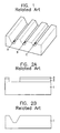
- a first SiN etching mask layer 2 and the first photoresist layer 3 are formed in succession on the silicon substrate 1, and a portion of the first SiN etching mask layer 2 is removed by photolithography and etching, to expose a region of the silicon substrate 1.
- the first SiN etching mask layer 2 is used as a mask in etching the silicon substrate 1 to an 'A' depth in FIG. 1, and the first SiN etching mask layer 2 and the first photoresist layer 3 are removed.
- FIG. 2B the first SiN etching mask layer 2 is used as a mask in etching the silicon substrate 1 to an 'A' depth in FIG. 1, and the first SiN etching mask layer 2 and the first photoresist layer 3 are removed.
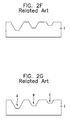
- a first SiN etching mask layer 12 and a first photoresist layer 13 are formed on a silicon substrate 11, and portions of the first SiN etching mask layer 12 are removed by photolithography and etching, to expose regions of the silicon substrate 1 to be etched as 'A', 'B' and 'C' in FIG. 1.
- the first SiN etching mask layer 12 is used as a mask in etching the exposed silicon substrate 11 in overall for the first time to a depth 'C' in FIG. 1 which has the shallowest etching depth, and the first SiN etching mask layer 12 and the first photoresist layer 13 are removed.
- FIG. 3B the first SiN etching mask layer 12 is used as a mask in etching the exposed silicon substrate 11 in overall for the first time to a depth 'C' in FIG. 1 which has the shallowest etching depth
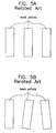
- a second SiN etching mask layer 14 and a second photoresist layer 15 are formed in succession on an entire surface of the substrate 11, and a portion of the second SiN mask layer 14 is removed by photolithography, to expose the silicon substrate 11 only in the 'B' region of FIG. 1.
- the second SiN etching mask layer 14 is used as a mask in etching the silicon substrate 11 etched for the first time for the second time, and the second SiN etching mask layer 14 and the second photoresist layer 15 are removed.
- a third SiN mask layer 16 and a third photoresist layer 17 are used in etching 'A' region in FIG. 1 etched for the first time for the second time by a method the same as the foregoing method, to complete fabrication of a device having different etching depths of'A', 'B' and 'C' as shown in FIG. 3G.
- the present invention is directed to an etching method that substantially obviates one or more of the problems due to limitations and disadvantages of the related art.
- the present invention provides an etching method for forming a plurality of trenches or recesses having depths different from one another in a substrate, comprising the steps of forming an etching mask on the substrate, forming a plurality of patterns in the etching mask corresponding to depths of the plurality of trenches, and etching the substrate using the etching mask having the plurality of patterns formed herein.
- the present invention provides an etching method including the steps of forming an etching mask on a substrate, etching a first, a second, and a third regions in the etching mask to a first depth on the same time, forming a first mask pattern in the first region, and using the first mask pattern as a mask in etching the second and third regions of the etching mask on the same time to a second depth, removing the first mask pattern, and forming second mask patterns in the first and second regions, etching the third region of the etching mask using the second mask patterns as a mask, to expose the substrate, removing the second mask patterns, and using the etching mask as a mask in etching the exposed substrate to a third depth, etching the second region of the etching mask to expose the substrate, and etching the exposed substrate to a fourth depth using the etching mask, and etching the first region of the etching mask to expose the substrate, and using the etching mask as a mask in
- the present invention provides an etching method, in which an etching mask formed for the first time is used in the next etching as it is. That is, as shown in FIG. 6, in fabrication of a device having different etch depths 'A', 'B' and 'C', the present invention provides an etching method which permits a simple and precise etching by using, not many etching masks as the case of the related art, but only one etching mask, applicable both to an wet etching and dry etching, and all kinds of wafers, etching solutions, and etching gases.
- an isotropic or an anisotropic etching of a silicon single crystal is possible depending on selected etching solution, which can be selected according to an etching purpose.
- HNA(HF + HNO 3 + Acetic Acid) is used as an isotropic etching solution
- EDP(Ethylenediamine Pyrocatechol Water), TMAH(Tetramethyl Ammonium Hydroxide), or KOH(Potassium Hydroxide) is used as an anisotropic etching solution.
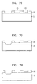
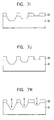
- the second photoresist pattern 24 is used as a mask in etching the SiN etching mask layer 22 to a required depth. Then, as shown in FIG. 7D, the second photoresist pattern 24 is removed, a third photoresist pattern 25 is respectively formed in the 'B' region and the 'C' region in FIG. 6 as shown in FIG. 7E, and the third photoresist patterns 25 are used as masks in dry etching as shown in FIG. 7F, to remove the SiN etching mask layer 22 only from 'A' region in FIG. 6, to expose the substrate 21. And, as shown in FIG.
- the third photoresist pattern 25 is removed, and the SiN etching mask layer 22 is used as a mask in wet etching the exposed substrate 21 to a depth.
- the SiN etching mask layer 22 is removed from the 'B' region in FIG. 6, to expose the substrate 21.
- the SiN etching mask layer 22 is used as a mask in wet etching the exposed substrate 21 to a depth, and the substrate 21 is dry etched on the whole without a photolithography process as shown in FIG. 7J, to remove the SiN etching mask layer 22 from the 'C' region in FIG.
- the SiN etching mask layer 22 is used as a mask again in wet etching the exposed substrate 21 to a depth, to obtain a silicon structure as shown in FIG. 6.
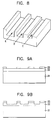
- 30wt% KOH water solution is used at a temperature of approx. 80°C.
- a surface of an (100) wafer is an (100) plane
- a side surface of the (100) wafer is an (111) plane, wherein the (111) plane is tilted by approx. 54.7° from the (100) plane.
- MEMS fabrication process there are many cases when a side surface at a right angle from the (100) plane wafer surface is required. In these cases, though a dry etching can make such a vertical side surface available, it is very difficult to conduct the dry etching by only using a photoresist pattern the same as the related art for obtaining the structure in FIG. 8. Accordingly, a dry etching by a method as shown in FIGS. 7A ⁇ 7B can make the structure as shown in FIG. 8 available with easy.
- FIGS. 9A ⁇ 9K illustrate sections showing the steps of a process for dry etching a silicon substrate, which are identical to FIGS. 7A ⁇ 7K, detailed explanations of which will be omitted.
- the etching mask layer 22 is formed of ITO(Indium Tin Oxide), and removed by using Cl 2 + BCl 3 gases.
- the silicon substrate 21 is etched using SF 6 gas and utilizing a high etching selectivity of the silicon substrate 21 over the etching mask layer 22.
- the present invention permits to form an SiN thin film as an etching mask only once for conducting etching over three times in formation of a silicon structure having three different depths, which is applicable to a dry etching, the present invention has a wide application.
- the elimination of an alignment error from respective photolithography by the present invention permits fabrication of a precise structure, to simplify a fabrication process, and to reduce a production cost.
Landscapes
- Micromachines (AREA)
- Drying Of Semiconductors (AREA)
- Weting (AREA)
Abstract
Description
Claims (7)
- An etching method for forming a plurality of trenches or recesses having depths different from one another in a substrate, comprising the steps of:forming an etching mask on the substrate;forming a plurality of patterns in the etching mask corresponding to depths ofthe plurality of trenches; and,etching the substrate using the etching mask having the plurality of patterns formed therein.
- An etching method, comprising the steps of:forming an etching mask on a substrate;etching a first, a second, and a third regions in the etching mask to a first depth on the same time;forming a first mask pattern in the first region, and using the first mask pattern as a mask in etching the second and third regions of the etching mask on the same time to a second depth;removing the first mask pattern, and forming second mask patterns in the first and second regions;using the second mask patterns as masks in etching the third region of the etching mask using the second mask patterns as a mask, to expose the substrate;removing the second mask patterns, and using the etching mask as a mask in etching the exposed substrate to a third depth;etching the second region of the etching mask to expose the substrate, and etching the exposed substrate to a fourth depth using the etching mask; and,etching the first region of the etching mask to expose the substrate, and using the etching mask as a mask in etching the exposed substrate to a fifth depth.
- A method as claimed in claim 2, wherein the substrate is etched either by wet etching or dry etching.
- A method as claimed in claim 3, wherein, in the wet etching, the etching mask is formed of SiN, and HNA(HF + HNO3 + Acetic Acid), EDP(Ethylenediamine Pyrocatechol Water), TMAH(Tetramethyl Ammonium Hydroxide), or KOH(Potassium Hydroxide) is used as an etching solution.
- A method as claimed in claim 3, wherein, in the dry etching, the etching mask is formed of ITO(Indium Tin Oxide), and SF6 is used an etching gas.
- A method as claimed in claim 2, wherein the first and second mask patterns are formed of photoresist.
- A Semiconductor device fabricated using the method of any preceding claim.
Applications Claiming Priority (2)
| Application Number | Priority Date | Filing Date | Title |
|---|---|---|---|
| KR1019990015492A KR100290852B1 (en) | 1999-04-29 | 1999-04-29 | method for etching |
| KR9915492 | 1999-04-29 |
Publications (2)
| Publication Number | Publication Date |
|---|---|
| EP1049143A2 true EP1049143A2 (en) | 2000-11-02 |
| EP1049143A3 EP1049143A3 (en) | 2000-12-27 |
Family
ID=19583004
Family Applications (1)
| Application Number | Title | Priority Date | Filing Date |
|---|---|---|---|
| EP00303661A Withdrawn EP1049143A3 (en) | 1999-04-29 | 2000-05-02 | Etching method |
Country Status (4)
| Country | Link |
|---|---|
| US (1) | US6458494B2 (en) |
| EP (1) | EP1049143A3 (en) |
| JP (1) | JP3363131B2 (en) |
| KR (1) | KR100290852B1 (en) |
Cited By (5)
| Publication number | Priority date | Publication date | Assignee | Title |
|---|---|---|---|---|
| US6458494B2 (en) * | 1999-04-29 | 2002-10-01 | Lg Electronics, Inc. | Etching method |
| DE10136016A1 (en) * | 2001-07-24 | 2003-04-03 | Bosch Gmbh Robert | Process for generating micromechanical structures |
| DE10154361A1 (en) * | 2001-11-06 | 2003-05-15 | Univ Albert Ludwigs Freiburg | Rapid prototyping process used in microstructures comprises applying etch-resistant coating to substrate, selectively removing the coating using a laser beam to produce at least one exposed region, and etching the exposed region |
| DE10311059A1 (en) * | 2003-03-13 | 2004-10-07 | Infineon Technologies Ag | Process for preparation of a semiconductor structure with troughs arranged in regions of different electrical conductivity useful in semiconductor technology, especially in miniaturizing processes |
| CN103258843A (en) * | 2013-05-30 | 2013-08-21 | 中国电子科技集团公司第十三研究所 | Multi-hole substrate for terahertz Schottky diode |
Families Citing this family (33)
| Publication number | Priority date | Publication date | Assignee | Title |
|---|---|---|---|---|
| US7064070B2 (en) | 1998-09-28 | 2006-06-20 | Tokyo Electron Limited | Removal of CMP and post-CMP residue from semiconductors using supercritical carbon dioxide process |
| US6890853B2 (en) | 2000-04-25 | 2005-05-10 | Tokyo Electron Limited | Method of depositing metal film and metal deposition cluster tool including supercritical drying/cleaning module |
| US6623653B2 (en) * | 2001-06-12 | 2003-09-23 | Sharp Laboratories Of America, Inc. | System and method for etching adjoining layers of silicon and indium tin oxide |
| US6939475B2 (en) * | 2001-08-31 | 2005-09-06 | Daishinku Corporation | Etching method, etched product formed by the same, and piezoelectric vibration device, method for producing the same |
| US6924086B1 (en) | 2002-02-15 | 2005-08-02 | Tokyo Electron Limited | Developing photoresist with supercritical fluid and developer |
| JP2006508521A (en) | 2002-02-15 | 2006-03-09 | 東京エレクトロン株式会社 | Drying of resist using solvent bath and supercritical CO2 |
| US7387868B2 (en) | 2002-03-04 | 2008-06-17 | Tokyo Electron Limited | Treatment of a dielectric layer using supercritical CO2 |
| CN1296771C (en) | 2002-03-04 | 2007-01-24 | 东京毅力科创株式会社 | Method of passivating of low dielectric materials in wafer processing |
| US7169540B2 (en) | 2002-04-12 | 2007-01-30 | Tokyo Electron Limited | Method of treatment of porous dielectric films to reduce damage during cleaning |
| DE10219398B4 (en) * | 2002-04-30 | 2007-06-06 | Infineon Technologies Ag | Manufacturing method for a trench arrangement with trenches of different depths in a semiconductor substrate |
| US7163380B2 (en) | 2003-07-29 | 2007-01-16 | Tokyo Electron Limited | Control of fluid flow in the processing of an object with a fluid |
| US6917093B2 (en) * | 2003-09-19 | 2005-07-12 | Texas Instruments Incorporated | Method to form shallow trench isolation with rounded upper corner for advanced semiconductor circuits |
| TWI266152B (en) * | 2003-12-30 | 2006-11-11 | Mosel Vitelic Inc | Mask and method of using the same |
| US20050244756A1 (en) * | 2004-04-30 | 2005-11-03 | Clarner Mark A | Etch rate control |
| US7307019B2 (en) | 2004-09-29 | 2007-12-11 | Tokyo Electron Limited | Method for supercritical carbon dioxide processing of fluoro-carbon films |
| US7491036B2 (en) | 2004-11-12 | 2009-02-17 | Tokyo Electron Limited | Method and system for cooling a pump |
| US7291565B2 (en) | 2005-02-15 | 2007-11-06 | Tokyo Electron Limited | Method and system for treating a substrate with a high pressure fluid using fluorosilicic acid |
| US7550075B2 (en) | 2005-03-23 | 2009-06-23 | Tokyo Electron Ltd. | Removal of contaminants from a fluid |
| KR100697283B1 (en) | 2005-03-29 | 2007-03-20 | 삼성전자주식회사 | Device isolation structure of semiconductor device and method of forming the same |
| US7442636B2 (en) | 2005-03-30 | 2008-10-28 | Tokyo Electron Limited | Method of inhibiting copper corrosion during supercritical CO2 cleaning |
| US7399708B2 (en) | 2005-03-30 | 2008-07-15 | Tokyo Electron Limited | Method of treating a composite spin-on glass/anti-reflective material prior to cleaning |
| US7789971B2 (en) | 2005-05-13 | 2010-09-07 | Tokyo Electron Limited | Treatment of substrate using functionalizing agent in supercritical carbon dioxide |
| EP2495212A3 (en) * | 2005-07-22 | 2012-10-31 | QUALCOMM MEMS Technologies, Inc. | Mems devices having support structures and methods of fabricating the same |
| US20070132056A1 (en) * | 2005-12-09 | 2007-06-14 | Advanced Analogic Technologies, Inc. | Isolation structures for semiconductor integrated circuit substrates and methods of forming the same |
| KR100901822B1 (en) * | 2007-09-11 | 2009-06-09 | 주식회사 실트론 | Gallium nitride growth substrate and gallium nitride substrate manufacturing method |
| KR101563684B1 (en) | 2008-11-10 | 2015-10-28 | 삼성전자주식회사 | Master for imprint and method of manufacturing the same |
| US8853091B2 (en) * | 2009-01-16 | 2014-10-07 | Microchip Technology Incorporated | Method for manufacturing a semiconductor die with multiple depth shallow trench isolation |
| US8227339B2 (en) | 2009-11-02 | 2012-07-24 | International Business Machines Corporation | Creation of vias and trenches with different depths |
| CN106477514B (en) * | 2015-08-28 | 2018-03-30 | 中芯国际集成电路制造(上海)有限公司 | MEMS devices and methods of forming them |
| EP3483938B1 (en) | 2016-07-06 | 2020-11-25 | Sony Semiconductor Solutions Corporation | Imaging element, method for producing imaging element, and electronic device |
| CN106229812B (en) * | 2016-08-31 | 2018-11-09 | 潍坊华光光电子有限公司 | A kind of preparation method of the GaAs base lasers with different depth groove |
| CN111208658A (en) * | 2020-03-02 | 2020-05-29 | 合肥鑫晟光电科技有限公司 | A transfer plate and preparation method thereof, display substrate and display panel |
| CN114551226A (en) * | 2020-11-26 | 2022-05-27 | 华为技术有限公司 | Method and system for preparing device with grooves with different depths |
Family Cites Families (11)
| Publication number | Priority date | Publication date | Assignee | Title |
|---|---|---|---|---|
| DE2535156C3 (en) * | 1975-08-06 | 1978-08-31 | Siemens Ag, 1000 Berlin Und 8000 Muenchen | Method for producing a layer with a predetermined pattern of regions of smaller layer thickness and using the layer as a mask for doping |
| US4139442A (en) * | 1977-09-13 | 1979-02-13 | International Business Machines Corporation | Reactive ion etching method for producing deep dielectric isolation in silicon |
| EP0286855A1 (en) * | 1987-04-15 | 1988-10-19 | BBC Brown Boveri AG | Process for etching moats in a silicon substrate |
| JPH043458A (en) * | 1990-04-19 | 1992-01-08 | Nec Corp | Formation of wiring of active layer laminated element |
| JPH0766276A (en) * | 1993-08-30 | 1995-03-10 | Canon Inc | Method for manufacturing semiconductor device |
| JPH08273990A (en) * | 1995-03-31 | 1996-10-18 | Toshiba Corp | Method for forming grooved Si substrate |
| JPH08279488A (en) * | 1995-04-05 | 1996-10-22 | Sony Corp | Method for manufacturing semiconductor device |
| US5738757A (en) * | 1995-11-22 | 1998-04-14 | Northrop Grumman Corporation | Planar masking for multi-depth silicon etching |
| US5958800A (en) * | 1996-10-07 | 1999-09-28 | Taiwan Semiconductor Manufacturing Company, Ltd. | Method for post planarization metal photolithography |
| JPH1145874A (en) * | 1997-07-25 | 1999-02-16 | Toshiba Corp | Method for manufacturing semiconductor device |
| KR100290852B1 (en) * | 1999-04-29 | 2001-05-15 | 구자홍 | method for etching |
-
1999
- 1999-04-29 KR KR1019990015492A patent/KR100290852B1/en not_active Expired - Fee Related
-
2000
- 2000-04-27 US US09/559,079 patent/US6458494B2/en not_active Expired - Fee Related
- 2000-05-01 JP JP2000132337A patent/JP3363131B2/en not_active Expired - Fee Related
- 2000-05-02 EP EP00303661A patent/EP1049143A3/en not_active Withdrawn
Cited By (7)
| Publication number | Priority date | Publication date | Assignee | Title |
|---|---|---|---|---|
| US6458494B2 (en) * | 1999-04-29 | 2002-10-01 | Lg Electronics, Inc. | Etching method |
| DE10136016A1 (en) * | 2001-07-24 | 2003-04-03 | Bosch Gmbh Robert | Process for generating micromechanical structures |
| EP1281663A3 (en) * | 2001-07-24 | 2005-03-02 | Robert Bosch Gmbh | Method of manufacture of micromechanical structures |
| DE10154361A1 (en) * | 2001-11-06 | 2003-05-15 | Univ Albert Ludwigs Freiburg | Rapid prototyping process used in microstructures comprises applying etch-resistant coating to substrate, selectively removing the coating using a laser beam to produce at least one exposed region, and etching the exposed region |
| DE10311059A1 (en) * | 2003-03-13 | 2004-10-07 | Infineon Technologies Ag | Process for preparation of a semiconductor structure with troughs arranged in regions of different electrical conductivity useful in semiconductor technology, especially in miniaturizing processes |
| CN103258843A (en) * | 2013-05-30 | 2013-08-21 | 中国电子科技集团公司第十三研究所 | Multi-hole substrate for terahertz Schottky diode |
| CN103258843B (en) * | 2013-05-30 | 2016-06-15 | 中国电子科技集团公司第十三研究所 | For the porous substrate of Terahertz schottky diode |
Also Published As
| Publication number | Publication date |
|---|---|
| JP3363131B2 (en) | 2003-01-08 |
| EP1049143A3 (en) | 2000-12-27 |
| KR100290852B1 (en) | 2001-05-15 |
| US6458494B2 (en) | 2002-10-01 |
| JP2000340553A (en) | 2000-12-08 |
| US20020008080A1 (en) | 2002-01-24 |
| KR20000067571A (en) | 2000-11-25 |
Similar Documents
| Publication | Publication Date | Title |
|---|---|---|
| US6458494B2 (en) | Etching method | |
| US7696045B2 (en) | Method of manufacturing semiconductor device | |
| EP2019081A2 (en) | Boron doped shell for MEMS device | |
| US8283256B1 (en) | Methods of forming microdevice substrates using double-sided alignment techniques | |
| JP2002237594A (en) | Thin film transistor, method of manufacturing thin film transistor, and display device including thin film transistor | |
| CN103137442B (en) | Method of manufacturing slender type isolated line patterns in semiconductor technology | |
| JPH06204776A (en) | Manufacture of piezoelectric thin film vibrator | |
| US8486608B2 (en) | Printing substrate for liquid crystal display, and manufacturing method thereof | |
| JPS61271839A (en) | Pattern formation method | |
| CN101459060A (en) | Method for manufacturing semiconductor device | |
| US6790699B2 (en) | Method for manufacturing a semiconductor device | |
| JP4465090B2 (en) | Manufacturing method of mask member | |
| US20130224958A1 (en) | Through hole forming method | |
| JP4994096B2 (en) | Semiconductor device manufacturing method and semiconductor device using the same | |
| US9373772B2 (en) | CMOS integrated method for the release of thermopile pixel on a substrate by using anisotropic and isotropic etching | |
| WO2003015183A1 (en) | Method for manufacturing thin-film structure | |
| US20070128757A1 (en) | Method for forming comb electrodes using self-alignment etching | |
| US7410901B2 (en) | Submicron device fabrication | |
| JP2786259B2 (en) | Method for manufacturing semiconductor device | |
| JP2005033192A (en) | Manufacturing method of semiconductor device | |
| JP3571843B2 (en) | Method for manufacturing hybrid optical integrated circuit | |
| KR19980054746A (en) | Pattern Separation Method of Semiconductor Device | |
| KR100237797B1 (en) | Method for manufacturing a semiconductor device having a deep trench | |
| JPH0117246B2 (en) | ||
| US20060104583A1 (en) | Method of fabricating ridge type waveguide integrated semiconductor optical device |
Legal Events
| Date | Code | Title | Description |
|---|---|---|---|
| PUAI | Public reference made under article 153(3) epc to a published international application that has entered the european phase |
Free format text: ORIGINAL CODE: 0009012 |
|
| AK | Designated contracting states |
Kind code of ref document: A2 Designated state(s): AT BE CH CY DE DK ES FI FR GB GR IE IT LI LU MC NL PT SE |
|
| AX | Request for extension of the european patent |
Free format text: AL;LT;LV;MK;RO;SI |
|
| PUAL | Search report despatched |
Free format text: ORIGINAL CODE: 0009013 |
|
| AK | Designated contracting states |
Kind code of ref document: A3 Designated state(s): AT BE CH CY DE DK ES FI FR GB GR IE IT LI LU MC NL PT SE |
|
| AX | Request for extension of the european patent |
Free format text: AL;LT;LV;MK;RO;SI |
|
| 17P | Request for examination filed |
Effective date: 20010531 |
|
| AKX | Designation fees paid |
Free format text: AT BE CH CY DE DK ES FI FR GB GR IE IT LI LU MC NL PT SE |
|
| 17Q | First examination report despatched |
Effective date: 20070605 |
|
| STAA | Information on the status of an ep patent application or granted ep patent |
Free format text: STATUS: THE APPLICATION IS DEEMED TO BE WITHDRAWN |
|
| 18D | Application deemed to be withdrawn |
Effective date: 20081202 |