EP1049000A2 - Logische Schaltungen und Uebertragvorgriffsschaltungen - Google Patents
Logische Schaltungen und Uebertragvorgriffsschaltungen Download PDFInfo
- Publication number
- EP1049000A2 EP1049000A2 EP00104483A EP00104483A EP1049000A2 EP 1049000 A2 EP1049000 A2 EP 1049000A2 EP 00104483 A EP00104483 A EP 00104483A EP 00104483 A EP00104483 A EP 00104483A EP 1049000 A2 EP1049000 A2 EP 1049000A2
- Authority
- EP
- European Patent Office
- Prior art keywords
- signals
- circuit
- signal
- group
- inversion
- Prior art date
- Legal status (The legal status is an assumption and is not a legal conclusion. Google has not performed a legal analysis and makes no representation as to the accuracy of the status listed.)
- Withdrawn
Links
Images


Classifications
-
- G—PHYSICS
- G06—COMPUTING; CALCULATING OR COUNTING
- G06F—ELECTRIC DIGITAL DATA PROCESSING
- G06F7/00—Methods or arrangements for processing data by operating upon the order or content of the data handled
- G06F7/38—Methods or arrangements for performing computations using exclusively denominational number representation, e.g. using binary, ternary, decimal representation
- G06F7/48—Methods or arrangements for performing computations using exclusively denominational number representation, e.g. using binary, ternary, decimal representation using non-contact-making devices, e.g. tube, solid state device; using unspecified devices
- G06F7/50—Adding; Subtracting
- G06F7/505—Adding; Subtracting in bit-parallel fashion, i.e. having a different digit-handling circuit for each denomination
- G06F7/506—Adding; Subtracting in bit-parallel fashion, i.e. having a different digit-handling circuit for each denomination with simultaneous carry generation for, or propagation over, two or more stages
- G06F7/508—Adding; Subtracting in bit-parallel fashion, i.e. having a different digit-handling circuit for each denomination with simultaneous carry generation for, or propagation over, two or more stages using carry look-ahead circuits
-
- A—HUMAN NECESSITIES
- A62—LIFE-SAVING; FIRE-FIGHTING
- A62C—FIRE-FIGHTING
- A62C35/00—Permanently-installed equipment
- A62C35/02—Permanently-installed equipment with containers for delivering the extinguishing substance
- A62C35/023—Permanently-installed equipment with containers for delivering the extinguishing substance the extinguishing material being expelled by compressed gas, taken from storage tanks, or by generating a pressure gas
-
- G—PHYSICS
- G06—COMPUTING; CALCULATING OR COUNTING
- G06F—ELECTRIC DIGITAL DATA PROCESSING
- G06F7/00—Methods or arrangements for processing data by operating upon the order or content of the data handled
- G06F7/74—Selecting or encoding within a word the position of one or more bits having a specified value, e.g. most or least significant one or zero detection, priority encoders
Definitions
- the present invention is related to a logic circuit for finding a "0" bit or a "1" bit by searching a binary bit string. Furthermore, the present invention is related to a carry-lookahead (CLA) circuit for use in arithmetic units handling a number of bits.
- CLA carry-lookahead
- logic circuits called a "0" bit searching circuit and a "1" bit searching circuit as logic circuits for constituting the hardware of a computer system.
- the logic circuits of this kind is used to find a "0" bit or a "1" bit by searching a binary bit string from the most significant bit to the least significant bit.
- the logic circuits are used to constitute a comparator for determining the largest number among a plurality of numbers, or a priority encoder used in a signal reception circuit having a plurality of input lines and provided, when receiving input signals at two or more input lines, for generating an output signal indicative of the input line receiving an input signal and having the highest priority among from the input lines receiving input signals.
- a "1" bit searching circuit in accordance with the prior art is composed of a number of the logic gate connected in a matrix form or in a tree arrangement so that the circuit design tends to be complicated. Furthermore, there are a number of gates arranged from the input to the output so that it takes much time to pass input data therethrough.
- carry lookahead circuits have been generally utilized in adder circuits for performing the addition operation of an N-bit input signal a ⁇ N-1 ⁇ , a ⁇ N-2 ⁇ , ... , a ⁇ 0 ⁇ ), referred to simply as a ⁇ N-1:0 ⁇ , and an N-bit input signal b ⁇ N-1 ⁇ , b ⁇ N-2 ⁇ , ..., b ⁇ 0 ⁇ , referred to simply as b ⁇ N-1:0 ⁇ .
- An example of such a prior art CLA circuit is described in Japanese Patent Published Application No.Hei 3-150630.
- the prior art carry lookahead circuit as described is a so-called carry select adder which performs the addition operation both in the case that the carry-in signal is "0" and in the case that the carry-in signal is "1". In accordance with the carry out from the lower bit operation, either result of the addition operation is selected and output as a correct result.
- Fig.3 is a block diagram showing an exemplary carry select adder which performs the addition operation both in the case that the carry-in signal is "0" and in the case that the carry-in signal is "1" and, in accordance with the carry out from the lower bit operation, either result of the addition operation is selected and output as a correct result.
- the carry lookahead circuit CLA1 serves to performs the addition operation in the case that the carry-in signal is "1" while the carry lookahead circuit CLA2 serves to performs the addition operation in the case that the carry-in signal is "0". Either of the outputs of the carry lookahead circuits CLA1 and CLA2 are selected by means of a 2-1 multiplexer MUX.
- a bit group 0 is arranged in the form of the 4-bit carry lookahead circuit as illustrated in Fig.2 in order to handle ⁇ 0:3 ⁇ bits of data having a 32 bit length to be handled while seven bit groups 1 to 7 are arranged in the form of the 4-bit carry lookahead circuits each designed as illustrated in Fig.3 in order to handle ⁇ 4:7 ⁇ bits, ⁇ 8:11 ⁇ bits, ⁇ 12:15 ⁇ bits, ... ⁇ 28:31 ⁇ bits of the data.
- a carry lookahead circuit capable of handling 32 bits is then formed as illustrated in Fig.1.
- C ⁇ 0 ⁇ to C ⁇ 3 ⁇ , C ⁇ 4 ⁇ to C ⁇ 7 ⁇ , C ⁇ 8 ⁇ to C ⁇ 11 ⁇ , ..., C ⁇ 28 ⁇ to C ⁇ 31 ⁇ are sequentially generated in this order in the group 0, the group 1, ... the group 7.
- Fig.4 shows the delay time required for completing the calculation, i.e., the delay time required for generating the carry signals C ⁇ 0 ⁇ to C ⁇ 31 ⁇ .
- Each of the carry lookahead circuits CLA1 and CLA2 of the respective carry lookahead circuits of the group 0 to the group 7 takes the same time T1 required for calculation.
- the multiplexer MUX of the carry lookahead circuit of the group 1 can initiate the operation required for selecting carry signals only after receiving the carry signal C ⁇ 3 ⁇ as given from the group 0.
- the delay time T2 of the multiplexer MUX is accumulated from the group 1 to the group 7 resulting in the total delay time T1+T2*7 . Because of this, in accordance with the prior art technique, there is a problem that a longer delay time is required for completing the calculation of carry signals for data having a longer bit sequence.
- the present invention has been made in order to solve the shortcomings as described above. It is an object of the present invention to provide logic circuits capable of performing high speed operations with simplified designs.
- a logic circuit for searching a binary bit string from the most significant bit to the least significant bit for a first "0" or "1" bit said logic circuit comprising:
- said NOT and NOR gate circuits are composed of NMOS FETs connected in parallel between the ground level and the output lines of said NOT and NOR gate circuits.
- a plurality of inverters are provided in advance of said 2-input NOR gate circuits.
- a logic circuit comprising:
- said first combinational logic circuit and said second combinational logic circuit have the same arrangement of constituent NMOS FETs.
- a pseudo-NMOS logic circuit comprising:
- a carry lookahead circuit for generating a group propagate signal PG and at least one of a group generate signal GG and a group kill signal KG for a group of m bits (m is an integer no less than 1) by the use of propagate signals P. generate signals G and kill signals K respectively for the constituent bits of the group, said carry lookahead circuit comprising:
- a carry lookahead circuit for generating a group propagate signal PG.
- a group carry signal CG and at least one of a group generate signal GG and a group kill signal KG for a group of m bits (m is an integer no less than 1) by the use of a carry signal C, propagate signals P. generate signals G and kill signals K respectively for the constituent bits of the group, said carry lookahead circuit comprising:
- a carry lookahead circuit comprising:
- Fig. 5 is a circuit diagram showing a priority encoder receiving a 4 bit signal to which the present invention is applied.
- the priority encoder 1 is provided for receiving input data of 4 bits each corresponding to different one of four input lines IN ⁇ 0 ⁇ , IN ⁇ 1 ⁇ , IN ⁇ 2 ⁇ and IN ⁇ 3 ⁇ and for outputting a 2 bits output code indicative of the input line having the highest priority among the four input lines.
- the priority encoder 1 is composed of a "1" bit searching circuit 2 accompanied with an encoder 3 for encoding the output signals S ⁇ 0 ⁇ , S ⁇ 1 ⁇ , S ⁇ 2 ⁇ and S ⁇ 3 ⁇ of the "1" bit searching circuit 2 into the 2 bits output code as output data Q0 and Q1.
- the input line having a smaller index has a higher priority.
- the priority level of the input line IN ⁇ 0 ⁇ is higher than that of the input line IN ⁇ 1 ⁇ .
- any conventional encoder can be used as an encoder 3 so that detailed explanation is dispensed with.
- the "1" bit searching circuit 2 serves to search a first "1" bit through the input data IN ⁇ 0 ⁇ , IN ⁇ 1 ⁇ , IN ⁇ 2 ⁇ and IN ⁇ 3 ⁇ in the priority order, i.e. from IN ⁇ 0 ⁇ to IN ⁇ 3 ⁇ .
- the "1" bit searching circuit 2 outputs a "1" bit as a Y output signal and the output data S ⁇ 0 ⁇ , S ⁇ 1 ⁇ , S ⁇ 2 ⁇ and S ⁇ 3 ⁇ in which a single bit S ⁇ i ⁇ (0 ⁇ i ⁇ 3) is "1", while the remaining bits S ⁇ j ⁇ (j ⁇ i) are "0".
- the "1" bit searching circuit 2 outputs a "0" bit as the Y output signal and the output data S ⁇ 0 ⁇ , S ⁇ 1 ⁇ , S ⁇ 2 ⁇ and S ⁇ 3 ⁇ of which all bits are "1".
- the "1" bit searching circuit 2 as illustrated in Fig.5 is composed of a NOT gate circuit 11 for receiving the input data IN ⁇ 0 ⁇ , a two-input NOT gate circuit 12 for receiving the input data IN ⁇ 0 ⁇ and IN ⁇ 1 ⁇ , a three-input NOT gate circuit 13 for receiving the input data IN ⁇ 0 ⁇ , IN ⁇ 1 ⁇ and IN ⁇ 2 ⁇ and a four-input NOT gate circuit 14 for receiving the input data IN ⁇ 0 ⁇ , IN ⁇ 1 ⁇ , IN ⁇ 2 ⁇ and IN ⁇ 3 ⁇ .
- the output signals of the NOT gate circuit 11 and the NOR gate circuits 12 to 14 are inverted by means of subsequent NOT gate circuits 15 to 18 and inverted again by means of NOT gate circuits 19 to 22, and then input to the input lines A0 to A3 of two-input NOR gate circuits 23 to 26.
- the input line B0 of the NOR gate circuit 23 is arranged to receive a bit signal of "0"
- the input line B1 of the NOR gate circuit 24 is arranged to receive the inversion signal of the NOT gate circuit 15
- the input line B2 of the NOR gate circuit 25 is arranged to receive the inversion signal of the NOT gate circuit 16
- the input line B3 of the NOR gate circuit 26 is arranged to receive the inversion signal of the NOT gate circuit 17.
- the result of the operation of the NOR gate circuits 23 to 26 is output as the output data S ⁇ 0 ⁇ , S ⁇ 1 ⁇ , S ⁇ 2 ⁇ and S ⁇ 3 ⁇ . Furthermore, the signal as inverted by means of the NOT gate circuit 18 is output as the output data Y.
- the bit sequence in the output side of the NOT gate circuit 11 and the NOR gate circuits 12 to 14 is "1000" while the bit sequence in the output side of the subsequent NOT gate circuits 15 to 18 is "0111".
- the operation of the "1" bit searching circuit 2 is conducted to search a binary bit string of the input data from the most significant bit to the least significant bit for finding a first "1” bit. i.e., a first bit pair of "01", followed by resetting all the subsequent bits to be "1".
- the "1" bit searching circuit 2 outputs the output data S ⁇ 0 ⁇ , S ⁇ 1 ⁇ , S ⁇ 2 ⁇ and S ⁇ 3 ⁇ as "0100" by passing the data through the NOT gate circuits 19 to 22 and the NOR gate circuits 23 to 26.
- the "1" bit searching circuit outputs "1000”, “0010” and “0001” in response to the input data "1XXX", “001X” and “0001” respectively, where X is either "0" or "1".
- the "1" bit searching circuit 2 serves to output a "1” bit as the output data Y if the input data IN ⁇ 3:0 ⁇ include a "1" bit.
- the output data S ⁇ 3:0 ⁇ is inputted to the encoder 3 and encoded into a 2 bits output code Q0 and Q1.
- the encoder 3 serves to output "00" indicative of the input line IN ⁇ 0 ⁇ for the output data S ⁇ 3:0 ⁇ of "1000", "01” indicative of the input line IN ⁇ 1 ⁇ for the output data S ⁇ 3:0 ⁇ of "0100", "10” indicative of the input line IN ⁇ 2 ⁇ for the output data S ⁇ 3:0 ⁇ of "0010", and "11” indicative of the input line IN ⁇ 3 ⁇ for the output data S ⁇ 3:0 ⁇ of "0001".
- the "1" bit searching circuit outputs a "0" bit as the output data Y
- the output data S ⁇ 3:0 ⁇ is assumed to be "0000" irrespective of the actual output of the encoder 3.
- the "1" bit searching circuit in accordance with this embodiment of the present invention can be designed in a simply fashion as compared with a "1" bit searching circuit in accordance with the prior art technique which is composed of a number of the logic gates connected in a matrix form or in a tree arrangement. Furthermore, there are fewer gates arranged one after another from the input to the output so that it takes a short time to pass input data therethrough. Accordingly, it is possible to realize logic circuits capable of performing high speed operations with simplified designs.
- Fig.6 is a circuit diagram showing the "1" bit searching circuit 2 as illustrated in Fig.5 in which the NOT gate circuit 11 and the NOR gate circuits 12 to 14 are composed of a dynamic logic circuit as enclosed with a broken line.
- the references PC0 to PC3 desingate PMOS FETs controlled by a clock signal (CLK) while the references N00 to N33 desingate NMOS FETs.
- the NMOS FET N00 corresponds to the NOT gate circuit 11; the NMOS FETs N10 and N11 correspond to the two-input NOR gate circuit 12; the NMOS FETs N20 to N22 correspond to the three-input NOR gate circuit 13; and the NMOS FETs N30 to N33 correspond to the four-input NOR gate circuit 14.
- Fig,7 is a circuit diagram showing the "1" bit searching circuit 2 in which NMOS FETs NC0 to NC3 are inserted to the dynamic logic circuit as illustrated in Fig.6 and enclosed with a broken line in order to dynamically enable the dynamic logic circuit in synchronism with the clock signal.
- the dynamic logic circuit 5 as illustrated in Fig.7 while the operation speed becomes slightly lower than in the case of the dynamic logic circuit as illustrated in Fig.6 and enclosed with a broken line, it is possible to prevent undesirable current from passing through the logic circuit during the precharging cycle responsive to the clock signal.
- Fig.8 is a circuit diagram showing the "1" bit searching circuit 2 in which a static circuit P0 to P7 are added to the dynamic logic circuit 5 as illustrated in Fig,7 in order to statically operate the dynamic logic circuit as enclosed with a broken line in synchronism with the clock signal.
- a static circuit P0 to P7 are added to the dynamic logic circuit 5 as illustrated in Fig,7 in order to statically operate the dynamic logic circuit as enclosed with a broken line in synchronism with the clock signal.
- the logic of the circuit is statically determined so that it is possible to stabilize the operation of the logic circuit.
- the operation speed of the logic circuit as illustrated in Fig.8 can be improved comparable to the operation speed of the logic circuit as illustrated in Fig.6.
- Fig.9 is a circuit diagram showing the "1" bit searching circuit 2 in which a static circuit P0 to P7 are added to the dynamic logic circuit 5 as illustrated in Fig.7 in order to statically operate the dynamic logic circuit as enclosed with a broken line and in which the clocked circuitry is eliminated.
- the logic of the circuit is statically determined so that it is possible to stabilize the operation of the logic circuit.
- the operation speed of the logic circuit as illustrated in Fig. 9 can also be improved comparable to the operation speed of the logic circuit as illustrated in Fig. 6 in the same manner.
- Fig. 11 is a circuit diagram showing a priority encoder receiving an input signal composed of a larger number of bits in accordance with the present invention by making use of a plurality of logic circuits having the same structure as the "1" bit searching circuit as illustrated in Fig.5.
- the priority encoder 31 is composed of a "1" bit searching circuit 32 and encoders 33a and 33b for encoding the output of the "1" bit searching circuit 32.
- the "1" bit searching circuit 32 is composed of four “1" bit searching circuits 2-1 to 2-4 capable of receiving 4-bit input data respectively, a "1" bit searching circuit 2-5 also capable of receiving 4-bit input data, an AND gate circuit 34 to 37 and a multiplexer 38.
- the "1" bit searching circuits 2-1 to 2-4 are provided in parallel, each of which serves to receive respective four bits of a 16-bit input data IN ⁇ 15:0 ⁇ .
- the "1" bit searching circuits 2-1 to 2-4 serve to generate Y0 ⁇ 3:0 ⁇ and SO ⁇ 15:0 ⁇ as intermediate output signals.
- the intermediate output signals Y0 ⁇ 3:0 ⁇ is input to the "1" bit searching circuit 2-5 while the intermediate output signals SO ⁇ 15:0 ⁇ are input to ones of the input lines of the AND gate circuits 34 to 37 and the input lines of the multiplexer 38.
- the "1" bit searching circuit 2-5 serves to generate an output data Y and intermediate output signals Y1 ⁇ 3:0 ⁇ .
- the intermediate output signals Y1 ⁇ 3:0 ⁇ are then input to the others of the input lines of the AND gate circuits 34 to 37 and the selection signal line of the multiplexer 38.
- the AND gate circuit serves to output the signals SO ⁇ 11:8 ⁇ when the intermediate output signal Y ⁇ 2 ⁇ is "1" and output the signals of "0000" when the intermediate output signal Y ⁇ 2 ⁇ is "0".
- the output data S ⁇ 15:0 ⁇ and the output Y1 ⁇ 3:0 ⁇ are equivalent to the logic circuit corresponding to the "1" bit searching circuit 2 illustrated in Fig.5 as extended to a 16 bit structure.
- the intermediate output signals T ⁇ 3:0 ⁇ are encoded by means of the encoder 33b in order to generate encoded output signals Q2 and Q3 while the intermediate output signals Y1 ⁇ 3:0 ⁇ are encoded by means of the encoder 33a in order to generate encoded output signals Q0 and Q1.
- the signals Q0, Q1, Q2 and Q3 are indicative of the position of a first "1" bit.
- the intermediate output signals Y1 ⁇ 3:0 ⁇ is encoded to "01” as encoded output signals Q2 and Q3 while the intermediate output signals T ⁇ 3:0 ⁇ is encoded to "10" as encoded output signals Q0 and Q1.
- the signals Q0, Q1, Q2 and Q3 are then indicative of the position "6" of a first "1" bit having the highest priority.
- the output data S ⁇ 15:0 ⁇ is assumed to be "0000000000000000" irrespective of the other output signals.
- Fig. 12 is a circuit diagram showing a carry lookahead circuit for use in a block adder circuit implemented with the "1" bit searching circuit as illustrated in Fig.5. Since the 4-1 encoder is not used here so that only the "1" bit searching circuit is utilized.
- the carry lookahead circuit is provided for receiving P (Propagate), G (Generate) and K (Kill) signals as input to the respective bits of the bit group to be handled by the carry lookahead circuit and calculating therefrom PG, PGB, GG and KG signals of the group.
- the carry lookahead circuit is composed of a 4-bit pseudo-NMOS NAND gate circuit 41, a 4-bit priority encoder PE and a 4-1 selector circuit SEL1.
- the pseudo-NMOS NAND gate circuit AN1 serves to calculate the PG (Propagate of Group) signal of the group on the basis of the P signals as input to the respective bits of the group.
- the priority encoder PE serves to calculate an output signal S ⁇ 3:0 ⁇ of the carry lookahead circuit and a PGB signal which is the inverted signal of the PG signal by the use of the PB signals, i.e., the inversion of the P signals, as input to the respective bits of the group.
- Fig.14 is a circuit diagram showing the priority encoder PE in which the constituent NOR gate circuits NR11, NR21 and NR31 are composed of a dynamic logic circuit as enclosed with a broken line.
- the selector circuit SEL1 is a dual-rail multiplexer comprising a 4-1 multiplexer MUX1 and a 4-1 multiplexer MUX2.
- the selector circuit SEL1 serves to calculate GG and KG signals by the use of the G and K signals as input to the respective bits of the group.
- Fig.14 is a circuit diagram showing the selector circuit SEL1 as composed of PMOS FETs, NMOS FETs and NOT gate circuits.
- Fig.16 shows a timing chart for explaining the input/output operation of the carry lookahead circuit as illustrated in Fig.12.
- the P signal as indicated with solid lines and the PB signal as indicated with broken lines on the input signals are precharged when the clock signal CLK is in the "L” level and then separated into complementary levels when the clock signal CLK is in the "H” level. Namely, the P signal takes a logic one while the PB signal takes a logic zero while the P signal takes a logic zero while the PB signal takes a logic one. Also, if the P signal takes a logic one, both the K signal as indicated with solid lines and the K signal as indicated with broken lines take a logic zero while if the PB signal takes a logic one, any one of the K signal and the K signal takes a logic zero.
- the PG, PGB, GG and KG signals of the group are output in the same timing as the PG, PB, G and K signals.
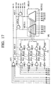
- Fig. 17 is a circuit diagram showing a carry lookahead circuit which is provided with AND gate circuits AN11 and AN12 in addition to the carry lookahead circuit as illustrated in Fig.12.
- the other constituent elements as illustrated in Fig.17 have the equivalent structures and functions of the counterparts as illustrated in Fig.12 and given the similar references.
- the carry lookahead circuit serves to calculate PG, PGB, GG and KG signals of the group and the CG group carry signal of the group to be output by the use of the P, G and K signals as input to the respective bits of the group and the C carry signals as input to the group.
- the carry lookahead circuit includes the AND gate circuit AN11 receiving the PGB signal and the output of the multiplexer MUX1 and the AND gate circuit AN12 receiving the PGB signal and the output of the the multiplexer MUX2.
- Fig.18 shows a timing chart for explaining the input/output operation of the carry lookahead circuit as illustrated in Fig.17.
- a plurality of the logic circuits as designed in the same manner as the carry lookahead circuit illustrated in Fig.12 or Fig.17 can be combined in a tree arrangement in order to form a larger carry lookahead circuit capable of handling a larger number of bits.
- the carry lookahead circuit as illustrated in Fig.17 is located in the output stage.
- a group generate signal GG and a group kill signal KG representing each group are calculated by the use of the propagate signals P ⁇ i ⁇ , the generate signals G ⁇ i ⁇ and the kill signals K ⁇ i ⁇ of the respective bits within each group.
- an input signal A and an input signal B are divided into four groups as follows.
- A (a15 to a12, a11 to a8, a7 to a4, a3 to a0)
- B (b15 to b12, b11 to b8, b7 to b4, b3 to b0)
- the carry signals C3, C7 and C11 for the respective groups will be obtained in accordance with the following equations.
- C3 f(a3 to a0, b3 to b0)
- C7 f(a7 to a4, b7 to b4)+C3
- C11 f(a11 to a7, b11 to b7)
- C7 C15 f(a15 to a11, b15 to b11)+C11
- Fig.12 is referred to again as a block diagram showing a first carry lookahead circuit CLA(1) for performing the required operation to generate the group signals PG, GG and KG.
- the first carry lookahead circuit CLA(1) serves to generate the group signals PG, GG and KG for the group of 4 bits.
- P ⁇ i ⁇ /a ⁇ i ⁇ */b ⁇ i ⁇
- G ⁇ i ⁇ a ⁇ i ⁇
- ExOR b ⁇ i ⁇ K ⁇ i ⁇ a ⁇ i ⁇ * b ⁇ i ⁇
- the first carry lookahead circuit CLA(1) is composed of an AND gate circuit AN1 serving to generate a signal PG. a priority encoder PE serving to generate selection signals S ⁇ 3:0 ⁇ and a selector circuit SEL1 serving to generate a signal GG and a signal KG.
- the AND gate circuit AN1 receives all the P ⁇ 3:0 ⁇ and perform the AND operation in accordance with the following equation (7) in order to output the signal PG and the signal PGB as the inversion of the signal PG.
- PG P ⁇ 3 ⁇ *P ⁇ 2 ⁇ *P ⁇ 1 ⁇ *P ⁇ 0 ⁇
- the signal GG and the signal KG are "0" respectively.
- the priority encoder PE is composed of a NOR gate circuit NR11 receiving the propagate signals PB ⁇ 3:0 ⁇ , an inverter IN11 and an inverter IN12 receiving the output of the NOR gate circuit NR11, a NOR gate circuit NR12 receiving the outputs of the inverters IN12 and IN21, a NOR gate circuit NR21 receiving the inversion of the propagate signals PB ⁇ 3:1 ⁇ , an inverter IN21 and an inverter IN22 receiving the output of the NOR gate circuit NR21, a NOR gate circuit NR22 receiving the outputs of the inverters IN22 and IN31, a NOR gate circuit NR31 receiving the inversion of the propagate signals PB ⁇ 3:2 ⁇ , inverters IN31 and IN32 receiving the output of the NOR gate circuit NR31, a NOR gate circuit NR32 receiving the outputs of the inverters IN32 and IN42, invert
- the selection signal S ⁇ 3:0 ⁇ is inputted to the selector circuit SEL1.
- the selector circuit SEL1 is composed of a multiplexer MUX1 and a multiplexer MUX2.
- the multiplexer MUX1 serves to receive the selection signal S ⁇ 3:0 ⁇ and select one of the signals G ⁇ 3:0 ⁇ corresponding to "1" in order to output the signal GG representing the group.
- the multiplexer MUX2 serves to receive the selection signal S ⁇ 3:0 ⁇ and select one of the signals K ⁇ 3:0 ⁇ corresponding to "1" in order to output the signal KG representing the group.
- the signal GG and the signal KG are also expressed by the use of the selection signal S ⁇ 3:0 ⁇ as follows.
- the selection signal S ⁇ 3:0 ⁇ are generated on the basis of the logics relating to the priority encoder as illustrated in Fig.12 and the logic equations (8) and (24) to (27).
- the equation (30) means that the logic for generating the signal GG can be implemented by a 4-1 multiplexer serving to select one of the signals G ⁇ 3:0 ⁇ in accordance with the selection signals S ⁇ 3:0 ⁇ .
- the equation (31) means that the logic for generating the signal KG can be implemented by a 4-1 multiplexer serving to select one of the signals K ⁇ 3:0 ⁇ in accordance with the selection signals S ⁇ 3:0 ⁇ .
- the first carry lookahead circuit CLA(1) serves to a group generate signals GG, a group generate signal GG and a group kill signal KG for a group of 4 bits by means of the AND gate circuit AN1, the priority encoder PE and the selector circuit SEL1.
- the circuit may be designed in order to generate only the signal PG and the signal GG or only the signal PG and the signal KG.
- the selector circuit SEL1 is composed only of the multiplexer MUX1.
- the selector circuit SEL1 is composed only of the multiplexer MUX2.
- the second carry lookahead circuit CLA(2) serves to generate not only the group propagate signal PG, the group generate signal GG and the group kill signal KG within the group, but also the group carry signal CG by the use of the group propagate signal PG, the group generate signal GG and the group kill signal KG. More specifically described, while the AND gate circuit AN1 and the priority encoder PE are designed in the same manner as those of the above embodiment as illustrated in Fig.12, a different type selector circuit SEL11 and AND gate circuits AN11 and AN12 are utilized.
- the selector circuit SEL11 is composed of a multiplexer MUX11 and a multiplexer MUX12.
- the multiplexer MUX11 receives the selection signal S ⁇ 3:0 ⁇ , the generate signals G ⁇ 3:0 ⁇ for respective bits as outputted from the priority encoder PE, the carry signal C from the previous (lower) group and the group propagate signals PG as outputted from the AND gate circuit AN1.
- the multiplexer MUX12 receives the selection signal S ⁇ 3:0 ⁇ , the generate signals K ⁇ 3:0 ⁇ for respective bits, the inversion of the carry signal CB as outputted from the previous (lower) group and the group propagate signals PG.
- the second carry lookahead circuit CLA(2) outputs the signal PG of "1" and the signal PGB of "0".
- the carry signal C as outputted from the previous (lower) group and the inversion of the carry signal CB are output as the group carry signal CG and the inversion of the group carry signal CGB, while the signal PGB is "0".
- the AND gate circuits AN11 and AN12 receiving the signal PGB serve to output the signal GG of "0" and the signal KG of "0" respectively.
- the signal PG is "0" and the signal PGB is "1".
- the generation of the signal CG and the signal CGB in this case is performed by selecting the signal G ⁇ i ⁇ and the signal K ⁇ i ⁇ corresponding to the selection signal S ⁇ i ⁇ taking "1” and outputting them as the group carry signal CG and the inversion of the group carry signal CGB.
- the AND gate circuit AN11 receiving the signal CG and the signal PGB taking "1” serves to generate the signal GG.
- the AND gate circuit AN12 receiving the signal CGB and the signal PGB taking "1" serves to generate the signal KG.
- CG PG*Cin+GG
- CG PG*Cin+S ⁇ 0 ⁇ *G ⁇ 0 ⁇ +S ⁇ 1 ⁇ *G ⁇ 1 ⁇ +S ⁇ 2 ⁇ *G ⁇ 2 ⁇ +S ⁇ 3 ⁇ *G ⁇ 3 ⁇
- CGB PG*/Cin+S ⁇ 0 ⁇ *K ⁇ 0 ⁇ +S ⁇ 1 ⁇ *K ⁇ 1 ⁇ +S ⁇ 2 ⁇ *K ⁇ 2 ⁇ +S ⁇ 3 ⁇ *K ⁇ 3 ⁇
- Fig.18 shows a timing chart for explaining the input/output operation of the second carry lookahead circuit CLA( 2).
- the solid lines designate the levels of the propagate signals P, the generate signals G and the kill signals K while the broken lines designate the levels of the levels of the inversion signals thereof PB, GB and KB.
- the signals P ⁇ 3:0 ⁇ , the signals G ⁇ 3:0 ⁇ and the signals K ⁇ 3:0 ⁇ are given together with the group carry signal C as outputted from the previous (lower) group in synchronism with the clock signal CLK.
- the group propagate signal PG, the group generate signal GG and the group kill signal KG are then outputted in the same timing with the delay time required for completing the operation.
- the circuit may be designed in order to generate only the signal PG, the signal GG and the signal CG or only the signal PG, the signal KG and the signal CGB.
- the selector circuit SEL11 is composed only of the multiplexer MUX1 for generating the signal CG through the AND gate circuit AN11.
- the selector circuit SEL11 is composed only of the multiplexer MUX2 for generating the signal KG through the AND gate circuit AN12.
- Fig.19 is a block diagram showing the configuration of the carry lookahead circuit by making use of both the first carry lookahead circuit CLA(1) as illustrated in Fig. 12 and the second carry lookahead circuit CLA(2) as illustrated in Fig.17.
- the carry lookahead circuit includes three group stages 0 to 2. the group stages 0 and 1 are composed of a plurality of the first carry lookahead circuits CLA(1) while the group stage 2 is composed of the second carry lookahead circuit CLA(2).
- the carry lookahead circuits belonging to the groups 7 to 0 serve to generate the signal PG ⁇ 7 ⁇ , GG ⁇ 7 ⁇ , KG ⁇ 7 ⁇ , PG ⁇ 6 ⁇ , GG ⁇ 6 ⁇ , KG ⁇ 6 ⁇ , ..., PG ⁇ 0 ⁇ , GG ⁇ 0 ⁇ and KG ⁇ 0 ⁇ in the group stage 0.
- the carry lookahead circuits in the group stage 1 are connected to the groups 7 to 4 and serve to generate the signal PGG ⁇ 1 ⁇ , GGG ⁇ 1 ⁇ , KGG ⁇ 1 ⁇ , PGG ⁇ 0 ⁇ , GGG ⁇ 0 ⁇ and KGG ⁇ 0 ⁇ for the groups 7 to 4 while the carry lookahead circuits belonging to the groups 3 to 0 also serve to generate the signal PGG ⁇ 1 ⁇ , GGG ⁇ 1 ⁇ , KGG ⁇ 1 ⁇ to PGG ⁇ 0 ⁇ , GGG ⁇ 0 ⁇ and KGG ⁇ 0 ⁇ .
- the signals PGGG, GGGG and KGGG for entire 32 bits are generated together with the final carry signal CGGG by means of the second carry lookahead circuit CLA(2).
- the signal CGGG corresponds to the carry signal C ⁇ 31 ⁇ .
- Fig. 20 is a graphic diagram showing the time required for completing the calculation in the carry lookahead circuit as designed above. If the group stage 0, the group stage 1 and the group stage 2 have the same delay time T11, the total delay time is T11*3. The total delay time T11*3 is the time accumulated through the three stages. Accordingly, it will be understood that the time required for completing the calculation is significantly reduced in accordance with the present invention as compared with the case in accordance with the prior art carry lookahead circuit as illustrated in Fig.4.
- the AND gate circuit AN1 is constructed as illustrated in Fig.13(b) by combining inverters and a pseudo-NMOS NAND gate circuit known as a pseudo-NMOS circuit as illustrated in Fig. 13(a).
- the NMOS FET N1 connected between the ground terminal and the node ND1 is turned on, when the clock signal CLK is in a low level, in order to discharge the node ND1.
- the PMOS FET is turned on while the NMOS FET N1 connected between the ground terminal and the node ND1 is turned off.
- the signals P ⁇ 3:0 ⁇ is inverted through the inverters IN104 to IN101 and inputted to the gates of the NMOS FETs N14 to N11 respectively connected between the node ND1 and the node ND2. Only when all the signals P ⁇ 3:0 ⁇ are "1", the NMOS FET N14 to N11 are turned off in order to discharge the node ND1 by means of the PMOS FET P1 and to generate the signal PG of "1". When at least one of the signals P ⁇ 3:0 ⁇ is "0", the FET receiving the "0" is turned on in order that the node ND1 is connected to the ground terminal by means of the PMOS FET P1 and that the signal PG of "0" is generated.
- the PMOS FET P1 is designed with such a narrow channel width that the node ND1 is pulled down near to the ground level, when only one of the NMOS FETs N11 to N14 is turned on, even if the PMOS FET P1 is turned on.
- the circuit operation can be improved by the use of the pseudo-NMOS AND circuit AN1 can be operated in synchronism with the clock signal CLK.
- Fig. 14 is a circuit diagram showing the priority encoder PE in which the constituent NOR gate circuits NR11, NR21 and NR31 are composed of a dynamic logic circuit as enclosed with a broken line for the first carry lookahead circuit CLA(1) as illustrated in Fig. 12 and the second carry lookahead circuit CLA(2) as illustrated in Fig.17.
- the priority encoder PE is driven in synchronism with the clock signal CLK in accordance with the dynamic operation.
- the signals PB ⁇ 3:0 ⁇ is input to a NOR gate circuit which is composed of PMOS FET P11 to P14 and NMOS FETs N21 to N32.
- the PMOS FETs P11 to P14 are connected between the power terminal and nodes ND11 to ND14 and controlled by the clock signal CLK applied to the clock signal CLK. When the clock signal CLK is in a low level, the nodes ND11 to ND14 are precharged.
- NMOS FET N21 to N24 are connected in parallel between the node ND11 and the node ND21 while an NMOS FET N25 is connected between the node ND21 and the ground terminal.
- NMOS FET N26 to N28 are connected in parallel between the node ND12 and the node ND22 while an NMOS FET N29 is connected between the node ND22 and the ground terminal.
- NMOS FETs N30 and N31 are connected in parallel between the node ND13 and the node ND23 while the NMOS FET N32 is connected between the NMOS FET N23 and the NMOS FET N32.
- an NMOS FET N33 is connected between the node ND14 and the node ND24 while the NMOS FET N34 is connected between the node ND24 the ground terminal.
- the clock signal CLK is input to the gate terminals of NMOSs FET N25, N29, N32 and N34.
- the signal PB ⁇ 0 ⁇ is input to the gate terminals of the NMOS FET N21.
- the signal PB ⁇ 1 ⁇ is input to the gate terminals of the NMOS FET N22 and the NMOS FET N26.
- the signal PB ⁇ 2 ⁇ is input to the gate terminals of NMOS FETs N23, N27 and, N30.
- the signal PB ⁇ 3 ⁇ is input to the gate terminals of NMOS FETs N24, N28, N31 and N33.
- the PMOS FETs P11 to P14 are turned on while the NMOS FETs N25, N29, N32 and N34 are turned off in order to charge the nodes ND11 to ND14.
- the NMOS FETs N25, N29, N32 and N34 are turned on in order to make it possible to discharge the nodes ND21 to ND 24.
- a high level signal is output through the node ND11 only in the case that all of the signals PB ⁇ 3:0 ⁇ are in logic "0” while a low level signal is output and is inverted by means of the inverter IN111 in order to generate the signal PGB in the case that at least one of the signals PB ⁇ 3:0 ⁇ is in the logic "1". Also, a high level signal is output through the node ND12 only in the case that all of the signals PB ⁇ 3:1 ⁇ are in logic "0” while a low level signal is output in the case that at least one of the signals PB ⁇ 3:0 ⁇ is in the logic "1".
- the low level signal is then inverted by means of the inverter IN113 and input to the NOR gate circuit NR101 together with the output of the inverter IN112 in order to generate the signal S ⁇ 0 ⁇ . Also, a high level signal is output through the node ND13 only in the case that all of the signals PB ⁇ 3:2 ⁇ are in logic "0" while a low level signal is output in the case that at least one of the signals PB ⁇ 3:2 ⁇ is in the logic "1". The low level signal is then inverted by means of the inverter IN115 and input to the NOR gate circuit NR102 together with the output of the inverter IN114 in order to generate the signal S ⁇ 1 ⁇ .
- a high level signal is output through the node ND14 only in the case that the signals PB ⁇ 3 ⁇ is in logic "0" while a low level signal is output in the case that the signal PB ⁇ 3 ⁇ is in the logic "1".
- the low level signal is then inverted by means of the inverter IN117 and input to the NOR gate circuit NR101 together with the output of the inverter IN116 in order to generate the signal S ⁇ 0 ⁇ .
- the output of the inverter IN117 is inverted by means of the inverter IN118 and inverted again by means of the NOR gate circuit NR104 in order to generate the signal S ⁇ 3 ⁇ .
- Figs.15(a) and Figs.15(b) are circuit diagrams showing the selector circuit SEL1 as composed of PMOS FETs, NMOS FETs and NOT gate circuits.
- the selector circuit SEL1 is composed of the multiplexer MUX1 as illustrated in Fig.15(a) and the multiplexer MUX2 as illustrated in Fig.15(b).
- the multiplexer MUX1 is constructed as follows.
- a PMOS FET P21 connected between the power terminal and the node ND31.
- the NMOS FETs N41 and N42 are connected in series between the node ND31 and the ground terminal.
- the NMOS FETs N43 to N48 is connected respectively in parallel between the NMOS FETs N41 and N42.
- the signals S ⁇ 0:3 ⁇ are input to the gate terminals of the NMOS FETs N41, N43, N45 and N47 while the signals G ⁇ 0:3 ⁇ are input to the gate terminals of the NMOS FETs N42, N44, N46 and N48.
- the PMOS FET P21 When the clock signal CLK is in a low level, the PMOS FET P21 is turned on in order to charge the node ND31.
- the node ND31 When the clock signal CLK is in a high level, the node ND31 is pulled down to the low level if at least one pair of signals S ⁇ 0 ⁇ and G ⁇ 0 ⁇ , signals S ⁇ 1 ⁇ and G ⁇ 1 ⁇ , signals S ⁇ 2 ⁇ and G ⁇ 2 ⁇ and signals S ⁇ 3 ⁇ and G ⁇ 3 ⁇ is ⁇ 1,1 ⁇ .
- the level of the node ND31 is inverted by means of the inverter IN121 in order to generate the signal GG.
- the multiplexer MUX2 has a corresponding configuration as the multiplexer MUX1 whose signals G ⁇ 0:3 ⁇ are replaced by the signals K ⁇ 0:3 ⁇ .
- the PMOS FET PT22 is connected between the power terminal and the node ND32.
- the NMOS FETs N51 and N52 are connected in series between the ground terminal and the node ND32.
- the NMOS FETs N41 and N42 are connected in series between the node ND31 and the ground terminal.
- the NMOS FETs N53 to N58 is connected respectively in parallel between the NMOS FETs N51 and N52.
- the signals S ⁇ 0:3 ⁇ are input to the gate terminals of the NMOS FETs N51, N53, N55 and N57 while the signals G ⁇ 0:3 ⁇ are input to the gate terminals of the NMOS FETs N52, N54, N56 and N58.
- the PMOS FET P22 When the clock signal CLK is in a low level, the PMOS FET P22 is turned on in order to charge the node ND32.
- the node ND32 When the clock signal CLK is in a high level, the node ND32 is pulled down to the low level if at least one pair of signals S ⁇ 0 ⁇ and K ⁇ 0 ⁇ . signals S ⁇ 1 ⁇ and K ⁇ 1 ⁇ , signals S ⁇ 2 ⁇ and K ⁇ 2 ⁇ and signals S ⁇ 3 ⁇ and K ⁇ 3 ⁇ is ⁇ 1,1 ⁇ .
- the level of the node ND32 is inverted by means of the inverter IN122 in order to generate the signal KG.
- the propagate signal P, the propagate signal G and the propagate signal K are generated for example by means of the logic circuits as illustrated in Fig.21(a) to Fig.21(d).
- Fig.21(a) shows a logic circuit for inputting an input signal A and an input signal B and the inversions of the input signal A and the input signal B and outputting the logic sum of the input signal A and the input signal B.
- the clock signal CLK is input to the gate terminals of a PMOS FET P31 in order to charge the node ND41 when the clock signal CLK is in a low level.
- the NMOS FET N63 is turned on.
- the signals A, /B, /A and B are input to the gate terminals of NMOS FET N61, N62, N64 and N65 in order to maintain the level of the node ND41 as selectively charged in accordance with the combination of the signals.
- the level of the node ND41 is inverted by means of the inverter IN131 and output as the signal P.
- Fig.21(b) shows a logic circuit for inputting an input signal A and an input signal B and the inversions of the input signal A and the input signal B and outputting the inversion of the logic sum of the input signal A and the input signal B.
- the logic circuit as illustrated in Fig.21(b) has a corresponding configuration as the logic circuit as illustrated in Fig.21(a) in which the gate terminals of NMOS FET N61, 62, 64 and 65 are adapted to receive A, B, /A and /B rather than A, /B, /A and B.
- Fig.21(c) shows a logic circuit for inputting an input signal A and an input signal B and outputting the logic product of the input signal A and the input signal B.
- the clock signal CLK is input to the gate terminals of a PMOS FET P33 in order to charge the node ND43 when the clock signal CLK is in a low level.
- the signals A and B are input to the gate terminals of the NMOS FET N81 and the NMOS FET N82 in order to maintain the level of the node ND41 as selectively charged in accordance with the combination of the signals.
- the NMOS FET N83 is turned on by the clock signal CLK.
- the level of the node ND43 is inverted by means of the inverter IN133 and output as the signal B.
- Fig.21(d) shows a logic circuit for inputting an input signal A and an input signal B and outputting the exclusive logic sum of the input signal A and the input signal B.
- the logic circuit as illustrated in Fig.21(d) has a corresponding configuration as the logic circuit as illustrated in Fig.21(c) in which the gate terminals of NMOS FET N81 and 82 are adapted to receive /A and /B rather than A, and B.
- Fig.1(a) is an exemplary circuit diagram composed of an AND gate circuit AN21 for generating the carry signal Cin for the respective constituent bits in synchronism with the clock signal CLK
- Fig.1(b) is an exemplary circuit diagram composed of an AND gate circuit AN22 and an inverter IN141 for generating the inversion of the carry signal /Cin for the respective constituent bits in synchronism with the clock signal CLK.
- the base bit strings can have a arbitrary number of bits and divided into a arbitrary number of groups.
- the AND gate circuit AN1, the priority encoder PE and the selector circuit SE may be modified in accordance with the actual cases.
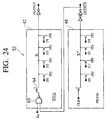
- Fig.23 is a circuit diagram showing a carry lookahead circuit in which the pseudo-NMOS NAND gate circuit 42 as illustrated in Fig.17 is connected to the "1" bit searching circuit 2-7.
- the other constituent elements as illustrated in Fig.24 have the equivalent structures and functions of the counterparts as illustrated in Fig.17 and given the similar references.
- the pseudo-NMOS NAND gate circuit 42 is connected to a dynamic logic circuit 46 as part of the "1" bit searching circuit 2-7 as illustrated in Fig 24.
- the pseudo-NMOS NAND gate circuit 42 and the dynamic logic circuit 46 have the same arrangement of constituent NMOS FETs.
- the pseudo-NMOS circuit 62 is composed of a plurality of NMOS FETs which are connected between the ground level and a signal line X in parallel under control of the inversion signal of the P signals of the respective bits of the group as given to the gate terminals of the NMOS FETs responsively, a PMOS gate circuit 47 connected to the signal line X in order to selectively connect the electric power source to the signal line X and an NAND gate circuit 48 connected to the PMOS gate circuit 47.
- the dynamic logic circuit 46 is composed of a plurality of NMOS FETs which are connected between the ground level and a signal line X* in parallel under control of the PB signals of the respective bits of the group as given to the gate terminals of the NMOS FETs responsively and a PMOS gate circuit 49 connected to the signal line X* in order to selectively connect the electric power source to the signal line X*.
- Fig.25 shows a timing chart for explaining the input/output operation of the pseudo-NMOS NAND gate circuit 42 as illustrated in Fig.24.
- the input signals to the pseudo-NMOS circuit 62 are pulled up to the "H” level during the precharge period (when the enable signal En is pulled down) in order to precharge the signal line X to the "L" level.
- the input signals to the dynamic logic circuit 46 is pulled down to the "L" level during the precharge period (when the clock signal CLK is pulled down) in order to precharge the signal line X* to the "H” level.
- the P signals of the respective bits of the group, i.e., P ⁇ 3:0 ⁇ and the PB signals of the respective bits of the group, i.e., PB ⁇ 3:0 ⁇ are then given to the input signals to the pseudo-NMOS circuit 62 and the input signals to the dynamic logic circuit 46 during the evaluation period.
- the enable signal En and the clock signal are pulled up during the evaluation period.
- the output of the control circuit 48 is a "1" so that the PMOS gate circuit 47 is turned on. All the input signals are then determinant during the next evaluation period. If the logic is not taken (i.e., the signal line X and the ground level are disconnected), the signal line X is maintained pulled up to the "H” level while there is no current as consumed therethrough. On the other hand, if the logic is taken (i.e., the signal line X and the ground level are connected), the signal line X is pulled down to the "L” level while there is a current as consumed through the PMOS gate circuit 47.
- the logic of the dynamic logic circuit 46 is also taken so that the signal line X* is pulled down to the "L” level and therefore the output signal OUTPUT* is also pulled down to the "L” level.
- the PMOS gate circuit 47 is then turned off by means of the control circuit 48 in order to prevent the undesirable idling current from flowing therethrough.
- FIG.A is a circuit diagram showing the combination of such a dynamic logic circuit and a pseudo-NMOS circuit of which output signals are correlated with each other.
- Fig.26 is a circuit diagram showing the combination of such a dynamic logic circuit and a pseudo-NMOS circuit of which output signals are correlated with each other.
- the pseudo-NMOS NAND gate circuit 62 and the dynamic logic circuit 66 have the same arrangement of constituent NMOS FETs in this example. However, as long as the signal line X and the signal line X* take the same logic value during the evaluation period, it is not an indispensable condition that the pseudo-NMOS NAND gate circuit 62 and the dynamic logic circuit 66 have the same arrangement of constituent NMOS FETs.
- the pseudo-NMOS circuit 62 is composed of a plurality of NMOS FETs which are connected between the ground level and a signal line X in parallel under control of the inversion signal of the P signals of the respective bits of the group as given to the gate terminals of the NMOS FETs responsively, a PMOS gate circuit 47 connected to the signal line X in order to selectively connect the electric power source to the signal line X and an WAND gate circuit 48 connected to the PMOS gate circuit 47.
- the dynamic logic circuit 46 is composed of a plurality of NMOS FETs which are connected between the ground level and a signal line X* in parallel under control of the PB signals of the respective bits of the group as given to the gate terminals of the NMOS FETs responsively and a PMOS gate circuit 49 connected to the signal line X* in order to selectively connect the electric power source to the signal line X*.
- Fig.27 shows a timing chart for explaining the input/output operation of the pseudo-NMOS WAND gate circuit 61 as illustrated in Fig.26.
- the signal INPUT[N:0] to be input to the pseudo-NMOS circuit 62 and the signal INPUT*[N:0] to be input to the dynamic logic circuit 63 take the same logic values during the evaluation period.
- the input signals INPUT[N:0] to the pseudo-NMOS circuit 62 is pulled up to the "H” level during the precharge period (when the enable signal En is pulled down) in order to precharge the signal line X to the "L" level.
- the input signals INPUT*[N:0] to the dynamic logic circuit 46 is pulled down to the "L" level during the precharge period (when the clock signal CLK is pulled down) in order to precharge the signal line X* to the "H” level.
- the logic signals to be evaluated are then given to the input signals to the pseudo-NMOS circuit 62 and the input signals to the dynamic logic circuit 46 during the evaluation period as INPUT[N:0] and INPUT*[N:0].
- the enable signal En and the clock signal are pulled up during the evaluation period.
- the output of the control circuit 48 is a "1" so that the PMOS gate circuit 47 is turned on. All the input signals are then determinant during the next evaluation period. If the logic is not taken (i.e., the signal line X and the ground level are disconnected), the signal line X is maintained pulled up to the "H” level while there is no current as consumed therethrough. On the other hand, if the logic is taken (i.e., the signal line X and the ground level are connected), the signal line X is pulled down to the "L” level while there is a current as consumed through the PMOS gate circuit 47.
- the logic of the dynamic logic circuit 46 is also taken so that the signal line X* is pulled down to the "L” level and therefore the output signal OUTPUT* is also pulled down to the "L” level.
- the PMOS gate circuit 47 is then turned off by means of the control circuit 48 in order to prevent the undesirable idling current from flowing therethrough.
- Fig.28 is a circuit diagram showing an example of a complementary logic circuit in accordance with the present invention by making use of pseudo-NMOS NAND gate circuits.
- the logic circuit 71 is composed of a first pseudo-NMOS circuit 72 and a second pseudo-NMOS circuit 73 whose output signal is complementary to the output of the first pseudo-NMOS circuit 72.
- the first pseudo-NMOS circuit 72 comprises a number of NMOS FETs combined to constitute a necessary logic as represented by a combinational logic circuit 72n and is supplied with the electric power source through the PMOS gate circuit 74 while the second pseudo-NMOS circuit 73 comprises a number of NMOS FETs combined to constitute a necessary logic as represented by a combinational logic circuit 73n and is supplied with the electric power source through the PMOS gate circuit 75.
- an NAND gate circuit 76 is provided for the first pseudo-NMOS circuit 72 to receive the output of the second pseudo-NMOS circuit 73 in order to selectively cut off the electric power supply to the first pseudo-NMOS circuit 72.
- an HAND gate circuit 76 is provided for the second pseudo-NMOS circuit 73 to receive the output of the first pseudo-NMOS circuit 72 in order to selectively cut off the electric power supply to the second pseudo-NMOS circuit 73.
- Fig.29 shows a timing chart for explaining the input/output operation of the complementary pseudo-NMOS NAND gate circuits illustrated in Fig.28.
- the signal to be input to the pseudo-NMOS circuit 72 and the signal to be input to the second pseudo-NMOS circuit 73 as gate signals to the constituent NMOS FETs can take arbitrary logic values as long as the pseudo-NMOS circuit 72 and the signal to be input to the second pseudo-NMOS circuit 73 output the complementary logic values during the evaluation period.
- the first pseudo-NMOS circuit 72 and the second pseudo-NMOS circuit 73 may given signal INPUT[N:0] and signal INPUT*[N:0] which take the complementary logic values during the evaluation period.
- the input signals INPUT[N:0] to the pseudo-NMOS circuit 72 and the input signals INPUT*[N:0] to the second pseudo-NMOS circuit 73 are commonly pulled up to the "H" level during the precharge period (when the enable signal En is pulled down) in order to precharge the signal line X and the signal line X* respectively to the "L" level.
- the output of the NAND gate circuit 76 is a "1" so that the PMOS gate circuit 74 is turned on during the evaluation period.
- the output signal OUTPUT* of the second pseudo-NMOS circuit 73 is precharged to the "H" level, the output of the NAND gate circuit 77 is a "1" so that the PMOS gate circuit 75 is turned on during the evaluation period when the enable signals En is activated. All the input signals are then determinant during the evaluation period.
- the logic of one of the combinational logic circuit 72n and the combinational logic circuit 73n is not taken (i.e., the signal line X (or X*) and the ground level are disconnected from the ground level) while the logic of the other of the combinational logic circuit 72n and the combinational logic circuit 73n is taken (i.e., the signal line X* (or X) and the ground level are connected from the ground level). Accordingly, since there is no current path serving to discharge the signal line X (or X*) of the combinational logic circuit being not taken, the signal line X (or X*) is maintained in the "H" level by means of the PMOS gate circuit 74 (or 75) resulting in no consumption current.
- Fig.29 is a circuit diagram showing an example of a complementary logic circuit in accordance with the present invention by making use of pseudo-NMOS NAND gate circuits as an application of the circuitry as illustrated in Fig.28.
- the logic circuit 81 is composed of a first pseudo-NMOS circuit 82 and a second pseudo-NMOS circuit 83 whose output signal is complementary to the output of the first pseudo-NMOS circuit 82.
- the first pseudo-NMOS circuit 82 comprises a number of NMOS FETs combined to constitute a necessary logic as represented by a combinational logic circuit 82n and is supplied with the electric power source through the PMOS gate circuit 84 while the second pseudo-NMOS circuit 83 comprises a number of NMOS FETs combined to constitute a necessary logic as represented by a combinational logic circuit 83n and is supplied with the electric power source through the PMOS gate circuit 85.
- the first pseudo-NMOS circuit 82 and the second pseudo-NMOS circuit 83 may given signal INPUT[N:0] and signal INPUT*[N:0] which take the complementary logic values during the evaluation period.
- an NAND gate circuit 86 is provided for the first pseudo-NMOS circuit 82 to receive the output of the second pseudo-NMOS circuit 83 in order to selectively cut off the electric power supply to the first pseudo-NMOS circuit 82. Also, an NAND gate circuit 86 is provided for the second pseudo-NMOS circuit 83 to receive the output of the first pseudo-NMOS circuit 82 in order to selectively cut off the electric power supply to the second pseudo-NMOS circuit 83.
- Fig.31 shows a timing chart for explaining the input/output operation of the complementary pseudo-NMOS NAND gate circuits illustrated in Fig.28.
- the signal to be input to the pseudo-NMOS circuit 82 and the signal to be input to the second pseudo-NMOS circuit 83 as gate signals to the constituent NMOS FETs can take arbitrary logic values as long as the pseudo-NMOS circuit 82 and the signal to be input to the second pseudo-NMOS circuit 83 output the complementary logic values during the evaluation period.
- the first pseudo-NMOS circuit 82 and the second pseudo-NMOS circuit 83 may given signal INPUT[N:0] and signal INPUT*[N:0] which take the complementary logic values during the evaluation period.
- the input signals INPUT[N:0] to the pseudo-NMOS circuit 82 and the input signals INPUT*[N:0] to the second pseudo-NMOS circuit 83 are commonly pulled up to the "H" level during the precharge period (when the enable signal En is pulled down) in order to precharge the signal line X and the signal line X* respectively to the "L" level.
- the output signal OUTPUT of the first pseudo-NMOS circuit 82 is precharged to the "H” level, the output of the NAND gate circuit 86 is a "1" so that the PMOS gate circuit 84 is turned on during the evaluation period.
- the output signal OUTPUT* of the second pseudo-NMOS circuit 83 is precharged to the "H" level, the output of the NAND gate circuit 87 is a "1" so that the PMOS gate circuit 85 is turned on during the evaluation period when the enable signals En is activated. All the input signals are then determinant during the evaluation period.
- the logic of one of the combinational logic circuit 82n and the combinational logic circuit 83n is not taken (i.e., the signal line X (or X*) and the ground level are disconnected from the ground level) while the logic of the other of the combinational logic circuit 82n and the combinational logic circuit 83n is taken (i.e., the signal line X* (or X) and the ground level are connected from the ground level). Accordingly, since there is no current path serving to discharge the signal line X (or X*) of the combinational logic circuit being not taken, the signal line X (or X*) is maintained in the "H" level by means of the PMOS gate circuit 84 (or 85) resulting in no consumption current.
Landscapes
- Engineering & Computer Science (AREA)
- Physics & Mathematics (AREA)
- General Physics & Mathematics (AREA)
- Theoretical Computer Science (AREA)
- General Engineering & Computer Science (AREA)
- Computational Mathematics (AREA)
- Mathematical Analysis (AREA)
- Pure & Applied Mathematics (AREA)
- Computing Systems (AREA)
- Mathematical Optimization (AREA)
- Health & Medical Sciences (AREA)
- Public Health (AREA)
- Business, Economics & Management (AREA)
- Emergency Management (AREA)
- Logic Circuits (AREA)
- Electronic Switches (AREA)
Applications Claiming Priority (4)
| Application Number | Priority Date | Filing Date | Title |
|---|---|---|---|
| JP6234699 | 1999-03-09 | ||
| JP06234699A JP3781573B2 (ja) | 1999-03-09 | 1999-03-09 | 論理回路 |
| JP18695699A JP3445533B2 (ja) | 1999-06-30 | 1999-06-30 | キャリールックアヘッド回路 |
| JP18695699 | 1999-06-30 |
Publications (2)
| Publication Number | Publication Date |
|---|---|
| EP1049000A2 true EP1049000A2 (de) | 2000-11-02 |
| EP1049000A3 EP1049000A3 (de) | 2006-05-10 |
Family
ID=26403407
Family Applications (1)
| Application Number | Title | Priority Date | Filing Date |
|---|---|---|---|
| EP00104483A Withdrawn EP1049000A3 (de) | 1999-03-09 | 2000-03-09 | Logische Schaltungen und Uebertragvorgriffsschaltungen |
Country Status (2)
| Country | Link |
|---|---|
| US (3) | US6329838B1 (de) |
| EP (1) | EP1049000A3 (de) |
Families Citing this family (13)
| Publication number | Priority date | Publication date | Assignee | Title |
|---|---|---|---|---|
| US6598066B1 (en) * | 2000-05-23 | 2003-07-22 | Sun Microsystems, Inc. | Fast carry-out generation |
| US6990508B1 (en) * | 2001-09-11 | 2006-01-24 | Cypress Semiconductor Corp. | High performance carry chain with reduced macrocell logic and fast carry lookahead |
| US6889235B2 (en) * | 2001-11-16 | 2005-05-03 | Apple Computer, Inc. | Method and apparatus for quantifying the number of identical consecutive digits within a string |
| US6621295B1 (en) * | 2002-01-15 | 2003-09-16 | Xilinx, Inc. | Reconfigurable priority encoding |
| JP3640643B2 (ja) * | 2002-01-18 | 2005-04-20 | 沖電気工業株式会社 | べき数エンコーダ回路及びマスク回路 |
| US7290027B2 (en) * | 2002-01-30 | 2007-10-30 | International Business Machines Corporation | Circuit suitable for use in a carry lookahead adder |
| US6972599B2 (en) | 2002-08-27 | 2005-12-06 | Micron Technology Inc. | Pseudo CMOS dynamic logic with delayed clocks |
| US7406495B2 (en) * | 2003-12-17 | 2008-07-29 | International Business Machines Corporation | Adder structure with midcycle latch for power reduction |
| US8086657B2 (en) * | 2004-10-26 | 2011-12-27 | International Business Machines Corporation | Adder structure with midcycle latch for power reduction |
| US20080109508A1 (en) * | 2006-10-19 | 2008-05-08 | Kenkare Prashant U | System having a carry look-ahead (cla) adder |
| US8214414B2 (en) * | 2008-09-30 | 2012-07-03 | Intel Corporation | Combined set bit count and detector logic |
| CN103185826B (zh) * | 2011-12-31 | 2016-09-14 | 意法半导体研发(深圳)有限公司 | 双向电压微分器电路 |
| JP6928698B1 (ja) * | 2020-08-05 | 2021-09-01 | ウィンボンド エレクトロニクス コーポレーション | 半導体装置および読出し方法 |
Citations (8)
| Publication number | Priority date | Publication date | Assignee | Title |
|---|---|---|---|---|
| US4570084A (en) * | 1983-11-21 | 1986-02-11 | International Business Machines Corporation | Clocked differential cascode voltage switch logic systems |
| EP0242600A2 (de) * | 1986-03-20 | 1987-10-28 | Kabushiki Kaisha Toshiba | Verfahren zur Berechnung des Übertragvorgriffs und Schaltung dazu |
| US4954978A (en) * | 1988-01-12 | 1990-09-04 | Mitsubishi Denki Kabushiki Kaisha | Priority order decomposing apparatus |
| US5187678A (en) * | 1989-09-30 | 1993-02-16 | Kabushiki Kaisha Toshiba | Priority encoder and floating-point normalization system for IEEE 754 standard |
| US5204825A (en) * | 1991-08-30 | 1993-04-20 | Weitek Corporation | Method and apparatus for exact leading zero prediction for a floating-point adder |
| WO1995000900A1 (en) * | 1993-06-22 | 1995-01-05 | Linköping University | An ultrafast adder arrangement |
| EP0707382A2 (de) * | 1994-09-20 | 1996-04-17 | Xilinx, Inc. | Schaltung und Logik für schnelle Übertragsrechnung |
| WO1997013201A1 (en) * | 1995-10-06 | 1997-04-10 | Advanced Micro Devices, Inc. | Unified multi-function operation scheduler for out-of-order execution in a superscalar processor |
Family Cites Families (9)
| Publication number | Priority date | Publication date | Assignee | Title |
|---|---|---|---|---|
| US4012722A (en) * | 1975-09-20 | 1977-03-15 | Burroughs Corporation | High speed modular mask generator |
| US4064421A (en) * | 1976-07-22 | 1977-12-20 | Burroughs Corporation | High speed modular arithmetic apparatus having a mask generator and a priority encoder |
| JPS64821A (en) * | 1987-06-23 | 1989-01-05 | Matsushita Electric Ind Co Ltd | Priority encoder |
| US5638009A (en) * | 1993-10-21 | 1997-06-10 | Sun Microsystems, Inc. | Three conductor asynchronous signaling |
| US5594368A (en) * | 1995-04-19 | 1997-01-14 | Kabushiki Kaisha Toshiba | Low power combinational logic circuit |
| JP3429927B2 (ja) | 1995-10-16 | 2003-07-28 | 三菱電機株式会社 | 浮動小数点演算装置の正規化回路装置 |
| US6078196A (en) * | 1997-09-17 | 2000-06-20 | Intel Corporation | Data enabled logic circuits |
| US6081914A (en) * | 1998-03-10 | 2000-06-27 | Xilinx, Inc. | Method for implementing priority encoders using FPGA carry logic |
| US6215325B1 (en) * | 1999-03-29 | 2001-04-10 | Synopsys, Inc. | Implementing a priority function using ripple chain logic |
-
2000
- 2000-03-08 US US09/521,620 patent/US6329838B1/en not_active Expired - Fee Related
- 2000-03-09 EP EP00104483A patent/EP1049000A3/de not_active Withdrawn
-
2001
- 2001-06-01 US US09/870,681 patent/US6362645B2/en not_active Expired - Fee Related
- 2001-06-01 US US09/870,687 patent/US6333644B2/en not_active Expired - Fee Related
Patent Citations (8)
| Publication number | Priority date | Publication date | Assignee | Title |
|---|---|---|---|---|
| US4570084A (en) * | 1983-11-21 | 1986-02-11 | International Business Machines Corporation | Clocked differential cascode voltage switch logic systems |
| EP0242600A2 (de) * | 1986-03-20 | 1987-10-28 | Kabushiki Kaisha Toshiba | Verfahren zur Berechnung des Übertragvorgriffs und Schaltung dazu |
| US4954978A (en) * | 1988-01-12 | 1990-09-04 | Mitsubishi Denki Kabushiki Kaisha | Priority order decomposing apparatus |
| US5187678A (en) * | 1989-09-30 | 1993-02-16 | Kabushiki Kaisha Toshiba | Priority encoder and floating-point normalization system for IEEE 754 standard |
| US5204825A (en) * | 1991-08-30 | 1993-04-20 | Weitek Corporation | Method and apparatus for exact leading zero prediction for a floating-point adder |
| WO1995000900A1 (en) * | 1993-06-22 | 1995-01-05 | Linköping University | An ultrafast adder arrangement |
| EP0707382A2 (de) * | 1994-09-20 | 1996-04-17 | Xilinx, Inc. | Schaltung und Logik für schnelle Übertragsrechnung |
| WO1997013201A1 (en) * | 1995-10-06 | 1997-04-10 | Advanced Micro Devices, Inc. | Unified multi-function operation scheduler for out-of-order execution in a superscalar processor |
Non-Patent Citations (3)
| Title |
|---|
| DELGADO-FRIAS J G ET AL: "A VLSI high-performance encoder with priority lookahead" VLSI, 1998. PROCEEDINGS OF THE 8TH GREAT LAKES SYMPOSIUM ON LAFAYETTE, LA, USA 19-21 FEB. 1998, LOS ALAMITOS, CA, USA,IEEE COMPUT. SOC, US, 19 February 1998 (1998-02-19), pages 59-64, XP010272629 ISBN: 0-8186-8409-7 * |
| LAI F-S ET AL: "DESIGN AND IMPLEMENTATION OF DIFFERENTIAL CASCODE VOLTAGE SWITCH WITH PASS-GATE (DCVSPG) LOGIC FOR HIGH-PERFORMANCE DIGITAL SYSTEMS" IEEE JOURNAL OF SOLID-STATE CIRCUITS, IEEE SERVICE CENTER, PISCATAWAY, NJ, US, vol. 32, no. 4, April 1997 (1997-04), pages 563-573, XP000659736 ISSN: 0018-9200 * |
| SOMASEKHAR D ET AL: "DIFFERENTIAL CURRENT SWITCH LOGIC: A LOW POWER DCVS LOGIC FAMILY" IEEE JOURNAL OF SOLID-STATE CIRCUITS, IEEE SERVICE CENTER, PISCATAWAY, NJ, US, vol. 31, no. 7, July 1996 (1996-07), pages 981-991, XP000632385 ISSN: 0018-9200 * |
Also Published As
| Publication number | Publication date |
|---|---|
| US20010032223A1 (en) | 2001-10-18 |
| US6329838B1 (en) | 2001-12-11 |
| US6362645B2 (en) | 2002-03-26 |
| EP1049000A3 (de) | 2006-05-10 |
| US6333644B2 (en) | 2001-12-25 |
| US20010037349A1 (en) | 2001-11-01 |
Similar Documents
| Publication | Publication Date | Title |
|---|---|---|
| EP1049000A2 (de) | Logische Schaltungen und Uebertragvorgriffsschaltungen | |
| US5661675A (en) | Positive feedback circuit for fast domino logic | |
| US5491653A (en) | Differential carry-save adder and multiplier | |
| Ruiz | Evaluation of three 32-bit CMOS adders in DCVS logic for self-timed circuits | |
| JPH02217920A (ja) | キヤリ・ルツクアヘツドを使用しているアダー | |
| US5163020A (en) | High speed BiCMOS conditional sum adder | |
| US20050182814A1 (en) | Encoder for a multiplier | |
| KR100221377B1 (ko) | 자동-리세팅 논리 회로, 멀티플렉서 회로 및 데이타 프로세싱 시스템 | |
| US5852568A (en) | System and method for a fast carry/sum select adder | |
| US6826588B2 (en) | Method and apparatus for a fast comparison in redundant form arithmetic | |
| US20040220994A1 (en) | Low power adder circuit utilizing both static and dynamic logic | |
| US6347327B1 (en) | Method and apparatus for N-nary incrementor | |
| US6782406B2 (en) | Fast CMOS adder with null-carry look-ahead | |
| US7290027B2 (en) | Circuit suitable for use in a carry lookahead adder | |
| US7206802B2 (en) | Hybrid carry look ahead/carry select adder including carry logic generating complementary hot carry signals, and method for producing the carry logic | |
| US5596520A (en) | CMOS full adder circuit with pair of carry signal lines | |
| US6334136B1 (en) | Dynamic 3-level partial result merge adder | |
| US6216147B1 (en) | Method and apparatus for an N-nary magnitude comparator | |
| KR100256103B1 (ko) | Cout 신호 발생용 방법 및 장치 | |
| Lai et al. | Design of a low latency asynchronous adder using early completion detection | |
| US6269387B1 (en) | Method and apparatus for 3-stage 32-bit adder/subtractor | |
| US6144228A (en) | Generalized push-pull cascode logic technique | |
| JP3445533B2 (ja) | キャリールックアヘッド回路 | |
| KR970703559A (ko) | 교번 극성 올림수 예측 가산기 회로(alternating polarity carry look ahead adder circuit) | |
| US20040220991A1 (en) | Faster shift value calculation using modified carry-lookahead adder |
Legal Events
| Date | Code | Title | Description |
|---|---|---|---|
| PUAI | Public reference made under article 153(3) epc to a published international application that has entered the european phase |
Free format text: ORIGINAL CODE: 0009012 |
|
| 17P | Request for examination filed |
Effective date: 20000309 |
|
| AK | Designated contracting states |
Kind code of ref document: A2 Designated state(s): AT BE CH CY DE DK ES FI FR GB GR IE IT LI LU MC NL PT SE |
|
| AX | Request for extension of the european patent |
Free format text: AL;LT;LV;MK;RO;SI |
|
| PUAL | Search report despatched |
Free format text: ORIGINAL CODE: 0009013 |
|
| AK | Designated contracting states |
Kind code of ref document: A3 Designated state(s): AT BE CH CY DE DK ES FI FR GB GR IE IT LI LU MC NL PT SE |
|
| AX | Request for extension of the european patent |
Extension state: AL LT LV MK RO SI |
|
| 17Q | First examination report despatched |
Effective date: 20060705 |
|
| AKX | Designation fees paid |
Designated state(s): DE FR GB |
|
| STAA | Information on the status of an ep patent application or granted ep patent |
Free format text: STATUS: THE APPLICATION IS DEEMED TO BE WITHDRAWN |
|
| 18D | Application deemed to be withdrawn |
Effective date: 20070116 |