EP1047227A2 - ATM switching system - Google Patents
ATM switching system Download PDFInfo
- Publication number
- EP1047227A2 EP1047227A2 EP00107175A EP00107175A EP1047227A2 EP 1047227 A2 EP1047227 A2 EP 1047227A2 EP 00107175 A EP00107175 A EP 00107175A EP 00107175 A EP00107175 A EP 00107175A EP 1047227 A2 EP1047227 A2 EP 1047227A2
- Authority
- EP
- European Patent Office
- Prior art keywords
- cell
- storage device
- temporal storage
- switching
- controller
- Prior art date
- Legal status (The legal status is an assumption and is not a legal conclusion. Google has not performed a legal analysis and makes no representation as to the accuracy of the status listed.)
- Granted
Links
Images



Classifications
-
- H—ELECTRICITY
- H04—ELECTRIC COMMUNICATION TECHNIQUE
- H04L—TRANSMISSION OF DIGITAL INFORMATION, e.g. TELEGRAPHIC COMMUNICATION
- H04L49/00—Packet switching elements
- H04L49/30—Peripheral units, e.g. input or output ports
-
- H—ELECTRICITY
- H04—ELECTRIC COMMUNICATION TECHNIQUE
- H04L—TRANSMISSION OF DIGITAL INFORMATION, e.g. TELEGRAPHIC COMMUNICATION
- H04L49/00—Packet switching elements
- H04L49/10—Packet switching elements characterised by the switching fabric construction
- H04L49/104—Asynchronous transfer mode [ATM] switching fabrics
- H04L49/105—ATM switching elements
- H04L49/106—ATM switching elements using space switching, e.g. crossbar or matrix
-
- H—ELECTRICITY
- H04—ELECTRIC COMMUNICATION TECHNIQUE
- H04L—TRANSMISSION OF DIGITAL INFORMATION, e.g. TELEGRAPHIC COMMUNICATION
- H04L49/00—Packet switching elements
- H04L49/25—Routing or path finding in a switch fabric
- H04L49/253—Routing or path finding in a switch fabric using establishment or release of connections between ports
- H04L49/254—Centralised controller, i.e. arbitration or scheduling
-
- H—ELECTRICITY
- H04—ELECTRIC COMMUNICATION TECHNIQUE
- H04L—TRANSMISSION OF DIGITAL INFORMATION, e.g. TELEGRAPHIC COMMUNICATION
- H04L49/00—Packet switching elements
- H04L49/25—Routing or path finding in a switch fabric
- H04L49/253—Routing or path finding in a switch fabric using establishment or release of connections between ports
- H04L49/255—Control mechanisms for ATM switching fabrics
-
- H—ELECTRICITY
- H04—ELECTRIC COMMUNICATION TECHNIQUE
- H04L—TRANSMISSION OF DIGITAL INFORMATION, e.g. TELEGRAPHIC COMMUNICATION
- H04L12/00—Data switching networks
- H04L12/54—Store-and-forward switching systems
- H04L12/56—Packet switching systems
- H04L12/5601—Transfer mode dependent, e.g. ATM
- H04L2012/5625—Operations, administration and maintenance [OAM]
- H04L2012/5627—Fault tolerance and recovery
-
- H—ELECTRICITY
- H04—ELECTRIC COMMUNICATION TECHNIQUE
- H04L—TRANSMISSION OF DIGITAL INFORMATION, e.g. TELEGRAPHIC COMMUNICATION
- H04L12/00—Data switching networks
- H04L12/54—Store-and-forward switching systems
- H04L12/56—Packet switching systems
- H04L12/5601—Transfer mode dependent, e.g. ATM
- H04L2012/5638—Services, e.g. multimedia, GOS, QOS
- H04L2012/5646—Cell characteristics, e.g. loss, delay, jitter, sequence integrity
- H04L2012/5649—Cell delay or jitter
-
- H—ELECTRICITY
- H04—ELECTRIC COMMUNICATION TECHNIQUE
- H04L—TRANSMISSION OF DIGITAL INFORMATION, e.g. TELEGRAPHIC COMMUNICATION
- H04L12/00—Data switching networks
- H04L12/54—Store-and-forward switching systems
- H04L12/56—Packet switching systems
- H04L12/5601—Transfer mode dependent, e.g. ATM
- H04L2012/5638—Services, e.g. multimedia, GOS, QOS
- H04L2012/5646—Cell characteristics, e.g. loss, delay, jitter, sequence integrity
- H04L2012/5651—Priority, marking, classes
-
- H—ELECTRICITY
- H04—ELECTRIC COMMUNICATION TECHNIQUE
- H04L—TRANSMISSION OF DIGITAL INFORMATION, e.g. TELEGRAPHIC COMMUNICATION
- H04L49/00—Packet switching elements
- H04L49/15—Interconnection of switching modules
- H04L49/1515—Non-blocking multistage, e.g. Clos
- H04L49/1523—Parallel switch fabric planes
-
- H—ELECTRICITY
- H04—ELECTRIC COMMUNICATION TECHNIQUE
- H04L—TRANSMISSION OF DIGITAL INFORMATION, e.g. TELEGRAPHIC COMMUNICATION
- H04L49/00—Packet switching elements
- H04L49/20—Support for services
- H04L49/205—Quality of Service based
-
- H—ELECTRICITY
- H04—ELECTRIC COMMUNICATION TECHNIQUE
- H04L—TRANSMISSION OF DIGITAL INFORMATION, e.g. TELEGRAPHIC COMMUNICATION
- H04L49/00—Packet switching elements
- H04L49/55—Prevention, detection or correction of errors
- H04L49/552—Prevention, detection or correction of errors by ensuring the integrity of packets received through redundant connections
Definitions
- the present invention relates to an ATM (Asynchronous Transfer Mode) switching system which is used for the sake of communication of the cell while multiplexing the cell efficiently.
- ATM Asynchronous Transfer Mode
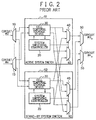
- Fig. 1 shows a conventional ATM (Asynchronous Transfer Mode) switching system.
- the conventional ATM switching system causes the system of an active system switch S1 (current application system) to be switched to a stand-by system switch S2 (subsequent application system) in accordance with the instruction of the microprocessor which is not illustrated.
- the microprocessor causes an input selector 10 connected to a circuit to execute switching such that only the input cell for respective switches S1, and S2 is switched to the subsequent application system.
- the stand-by system switch S2 stores therein the input cell while stopping output operation temporarily until when the whole cells are sent out from the inside of the cell temporal storage device 30 on the inside of the active system switch S1.
- a vacancy monitor 70 monitors the inside of the cell temporal storage device 30.
- a result of the monitoring according to the vacancy monitor 70 informs that there is vacant port. According to the monitoring result, an output operation of the stand-by system is permitted in order of the port whose cell temporal storage device 30 of the active system becomes vacant. Simultaneously, the output selector 50 in the output side executes switching, thus causing the output cell from the stand-by system to be transmitted to the circuit.
- the cell temporal storage device 30 of the whole output ports of the active system becomes vacant, before the output operation of the cell is commenced from the whole output ports of the stand-by system. On this occasion, sequence of the system switching ends, thus returning to stationary operation. According to these operation, switching becomes possible without occurrence of loss of the cell even though at the time when the duplicate switches are switched.
- a delay priority selector 40 is introduced so as to add the delay priority selector 40 to the constitution of Fig. 1.
- a system switching controller 20 instead of the vacancy monitor 70.
- the cell At the time of switching of the system, it causes the cell to be read in order of height of delay priority from among the cells stored in both of temporal storage devices of the active system and the stand-by system.
- Such the switching system is disclosed in the official report of the Japanese Patent Application Laid-Open No. HEI 11-17696.
- ITU-T recommendation or the document of The ATM Forum defines both characteristic of the above delay priority and abolition priority by using term Quality of Service (hereinafter referred to as "QoS").
- the cell with high delay priority is always outputted while giving the cell priority during executing system switching. For that reason, the cell with low delay priority becomes difficult to be read-out from the cell temporal storage device 30 of the active system. Further, unless the whole cells are outputted, which cells are stored in the cell temporal storage device 30 of the active system, the system switching is not completed yet. Thus, there is the problem that the time elapsing for the sake of system switching increases. Namely, the cell of the traffic class (for instance CBR: Constant Bit Rate) whose outgoing destination is settled beforehand in regard to bandwidth to be used occupies this bandwidth of the circuit fully.
- CBR Constant Bit Rate
- the cell of the traffic class (for instance ABR : Address Base Resistor or VBR : Variable Bit Rate) is not outputted, whose bandwidth reservation is not performed beforehand in regard to outgoing destination, stored in the cell temporal storage device 30 of the active system.
- the system switching is not completed. Consequently, forced switching according to timeout of the software is executed.
- abolition of the cell of the ABR traffic with high abolition priority occurs.
- an ATM (Asynchronous Transfer Mode) switching system which comprises an input selector for dividing cell inputted from a circuit between an active system switch and a stand-by system switch, a system switching controller which is provided for the active system switch and the stand-by system switch respectively in order to execute control of system switching, a cell temporal storage device which is provided for the active system switch and the stand-by system switch respectively for storing temporarily therein the inputted cell in every service quality class or in every outgoing destination, a delay priority selector for reading-out the cell with high delay priority successively to output from the respective cell temporal storage device under control of the system switching controller, and an output selector for outputting the cell of the delay priority selector to circuit, wherein the ATM switching system causes output of the cell to be executed for the sake of the delay priority selector from the cell temporal storage device of active system after condition that there becomes none of the cell whose delay priority is higher than that of the cell stored in the active system
- an ATM switching system wherein it causes the cell of class of low abolition priority stored in the cell temporal storage device of the active system to be abolished after elapsing fixed time from commencement of system switching in the condition that the cell with low delay priority is stored in the cell temporal storage device of the active system.
- an ATM switching system wherein the cell temporal storage device comprises a quality of service demultiplexer for separating an input cell obtained from the input selector in every quality of service class, a cell temporal storage memory for storing the input cell obtained from the quality of service demultiplexer temporarily in every quality of service class, a write controller for controlling write of the input cell for the cell temporal storage memory, a read controller for reading to be controlled the input cell whose arrival time is the most earliest arrival time among quality of service class on the occasion of reception of the quality of service class information from the system switching controller, and a cell abolition controller for implementing instruction with regard to the write controller and the read controller that it causes the whole cells of the quality of service class to be abolished on the occasion of reception of the quality of service class information from the system switching controller.
- the cell temporal storage device comprises a quality of service demultiplexer for separating an input cell obtained from the input selector in every quality of service class, a cell temporal storage memory for storing the input cell obtained from the quality of service demultiplex
- an ATM switching system wherein the system switching controller comprises a cell management part for instructing read-out of the cell whose delay priority is the most highest delay priority among the cell stored in the cell temporal storage device of sell-system and / or another system, a selector controller for controlling the delay priority selector so as to select the cell from either sell-system cell temporal storage device or another system cell temporal storage device, an another system communication part for implementing coordination that it causes which cell of delay class to be stored in the sell-system cell temporal storage device and the another system cell temporal storage device, and that it causes read-out of which cell of delay class to be implemented, and a timer for instructing abolition of the cell of lower class of cell abolition priority with regard to the cell temporal storage device after elapsing fixed time from commencement of the system switching.
- the system switching controller comprises a cell management part for instructing read-out of the cell whose delay priority is the most highest delay priority among the cell stored in the cell temporal storage device of sell-system and / or another system,
- an ATM switching system wherein the cell temporal storage memory is used commonly in the quality of service class.
- an ATM switching system wherein the cell temporal storage memory is a first-in first-out memory.
- an ATM link switching method which comprises the steps of, a step for dividing cell inputted from a circuit between an active system switch and a stand-by system switch by using an input selector, a step for executing control of system switching by a system switching controller which is provided for the active system switch and the stand-by system switch respectively, a step for storing temporarily therein the inputted cell in every service quality class or in every outgoing destination by a cell temporal storage device which is provided for the active system switch and the stand-by system switch respectively, a step for reading-out the cell with high delay priority successively to output from the respective cell temporal storage device under control of the system switching controller by a delay priority selector, and a step for outputting the cell of the delay priority selector to circuit by an output selector, wherein the ATM switching system causes output of the cell to be executed for the sake of the delay priority selector from the cell temporal storage device of active system after condition that there becomes none of the cell whose delay priority is higher than that of the
- an ATM link switching method wherein operating method of the cell temporal storage device comprises the steps of a step for separating an input cell obtained from the input selector in every quality of service class by a quality of service demultiplexer, a step for storing the input cell obtained from the quality of service demultiplexer temporarily in every quality of service class by a cell temporal storage memory a step for controlling write of the input cell for the cell temporal storage memory by a write controller, a step for reading to be controlled the input cell whose arrival time is the most earliest arrival time among quality of service class on the occasion of reception of the quality of service class information from the system switching controller by a read controller, and a step for implementing instruction with regard to the write controller and the read controller that it causes the whole cells of the quality of service class to be abolished on the occasion of reception of the quality of service class information from the system switching controller by a cell abolition controller.
- an ATM link switching method wherein operating method of the system switching controller comprises the steps of a step for instructing read-out of the cell whose delay priority is the most highest delay priority among the cell stored in the cell temporal storage device of self-system and / or another system by a cell management part, a step for controlling the delay priority selector so as to select the cell from either self-system cell temporal storage device or another system cell temporal storage device by a selector controller, a step for implementing coordination that it causes which cell of delay class to be stored in the self-system cell temporal storage device and the another system cell temporal storage device, and that it causes read-out of which cell of delay class to be implemented by an another system communication part, and a step for instructing abolition of the cell of lower class of cell abolition priority with regard to the cell temporal storage device after elapsing fixed time from commencement of the system switching by a timer.
- Fig. 3 is a block diagram showing an ATM switching system according to one embodiment of the present invention.
- the ATM switching system comprises an input selector 10 for dividing the cell inputted from a circuit between an active system switch S1 and stand-by system switch S2, a system switching controller 20 for implementing control on the occasion of system switching while being provided for the active system switch S1 and the stand-by system switch S2 of respective systems, a cell temporal storage device 30 for storing temporarily an input cell therein inputted through the input selector 10 in every delay class, a delay priority selector 40 for selecting either the active system switch or the stand-by system switch from which it causes the cell of the certain delay priority class to be outputted, and an output selector 50 for outputting the cell from the active system switch S1 operating as a current active system switch or the stand-by system switch.
- Fig. 4 is a block diagram showing detail of the system switching controller 20 shown in Fig. 3.
- the system switching controller 20 comprises a cell managing part 21 for outputting output instruction while waiting cell information stored in the cell temporal storage device 30, a selector controller 22 for controlling selection that it causes the cell to be outputted from which cell temporal storage devices 30, a communication part among another system 23 for executing mediation that it causes read-out of the cell for the sake of which delay class to be implemented from between both cell temporal storage devices 30 in which respective cells of delay class are stored, and a timer for instructing abolition of the cell to the cell temporal storage device, after fixed time elapsing from commencement of system switching.
- Fig. 5 is a block diagram showing details of the cell temporal storage device 30 shown in Fig. 3.
- a demultiplexer (DEMUX) 31 separates the cell in every respective "QoS" (Quality of Service) class.
- a cell temporal storage memory 32 stores the cell therein temporarily in every respective "QoS” class.
- a write controller 33 manages write address of the cell.
- a read controller 34 manages readout address of the cell.
- a "QoS" multiplexer (MUX) 35 multiplexes an output cell in every respective "QoS" class.
- a cell abolition controller 36 executes cell abolition according to cell abolition instruction from the system switching controller 20.
- the form of the ATM switch is capable of being classified roughly into an input buffer type ATM switch, an output buffer type ATM switch, an input / output buffer type ATM switch, and shared buffer type ATM switch. This is well known by the authorities concerned. Further, this is not related to the present invention directly, thus, the position of the ATM switch is omitted.
- the input cell passes through only within an active system device, and there is none inflow / storage of the cell for a stand-by system device.
- the cell is inputted from a circuit.
- the input selector 10 transmits the cell to the active system (current operation system) switch S1.
- the transmitted cell is divided in every "QoS" class.
- the divided cell is stored in the cell temporal storage device 30 in every "QoS” class.
- the system switching controller 20 executes instruction that it causes the cell with high delay priority to be read while giving it priority from among the cells stored for the cell temporal storage device 30.
- the cell is read-out in order of height of delay priority.
- the cell with the highest delay priority is read-out in the first place.
- the cell is read-out in every delay priority class.
- the respective cells in accordance with the delay priority pass through the delay priority selector 40.
- the output selector 50 causes the cell to pass through current active system side to output to the circuit.
- the cell passes through the current active system side before being outputted to the circuit.
- the system switching controller 20 operates as follows.
- the cell is stored in the cell temporal storage device 30.
- the cell of the respective delay classes is stored therein with respective quantities.
- the information of respective quantities is noticed to the cell management part 21.
- the information is that the respective delay classes store therein how much quantities of the cell.
- the quantities of the cell in every respective delay classes are noticed to the cell management part 21.
- the cell management part 21 receives cell storage condition of the cell temporal storage device 30 of another system through the communication part among another system 23.
- the cell management part 21 transmits information of self-system.
- the cell management part 21 instructs read-out of the cell with the highest delay priority from among the cells stored in both of self-system / another system.
- the cell management part 21 executes read-out instruction for the cell temporal storage device 30 of the self-system.
- the cell management part 21 executes instruction to the selector controller 22 so as to read-out the cell concerned from the self-system too.
- the cell management part 21 executes read-out instruction for the cell temporal storage device 30 of another system through the communication part among another system 23.
- the cell management part 21 executes instruction to the selector controller 22 so as to read-out the cell concerned from another system too.
- the timer 24 executes abolition instruction of the cell to the cell temporal storage device 30 of the self-system.
- the abolition instruction of the cell is implemented in every respective "QoS" class.
- the abolition instruction according to the timer 24 is executed after elapsing times set beforehand, with start of system switching as trigger. Thus, it causes the cell of lower class of cell abolition priority to be abolished with respect to the cells stored in the cell temporal storage device 30 of the self-system.
- the cell temporal storage device 30 of Fig. 5 operates as follows. Firstly, the cell temporal storage device 30 inputs therein the cell.
- the "QoS” demultiplexer 31 detects "QoS” class of the cell.
- the "QoS” demultiplexer 31 transmits the cell for the different cell temporal storage memory 32 in every "QoS” class.
- the cell temporal storage memory 32 causes the received cell to be stored in address indicated by the write controller 33.
- the read controller 34 receives a "QoS" class information from the system switching controller 20, the read controller 34 executes a read-out instruction of the cell having the earliest arrival time among the "QoS" classes.
- the cell abolition controller 36 receives abolition "QoS" class information from the system switching controller 20. On this occasion, the cell abolition controller 36 executes instruction causing the whole cells to be abolished with respect to the "QoS" class to the write controller 33 and the read controller 34.
- FIFO First-In First-Out
- the cell with low delay priority is stored in the cell temporal storage device 30 of the active system of the current operation system.
- the cell with higher delay priority than that of the above cell is stored successively in the cell temporal storage device 30 of the stand-by system of subsequent operation system.
- the system switching controller 20 causes the timer 24 to be triggered, before implementing management of both of the cell temporal storage device 30 of the active system and the cell temporal storage device 30 of the stand-by system.
- the system switching controller 20 executes read-out of the cell whose delay priority is high between both devices. Namely, in this case, firstly the read-out of the cell is implemented from the cell temporal storage device 30 of this stand-by system of the subsequent operation system.
- the cell whose delay priority is higher than that of the cell stored in the cell temporal storage device 30 of active system decreases at the cell temporal storage device 30 of the stand-by system. It causes a cell output operation to be executed from the cell temporal storage device 30 of the active system at the time when there becomes none storage of the cell whose delay priority is higher than that of the cell stored in the cell temporal storage device of the active system.
- the delay priority selector 40 executes selection in accordance with control of the system switching controller 20. The selection is implemented whether an output from the active system device is selected or an output from the stand-by system device is selected, in every respective delay classes. Either the output from the active system or the output of the stand-by system is transmitted to the output selector 50.
- the cell with low delay priority is stored in the cell temporal storage device 30 of the active system.
- the system switching controller 20 implements abolition instruction of the cell of the low class of the abolition priority stored within the cell temporal storage device 30 of the active system.
- the system switching controller 20 instructs abolition with respect to the cell temporal storage device 30 of the active system as the current application system.
- the cell with low abolition priority is abolished.
- it is capable of providing a system which executes switching the duplicate switch in short time while maintaining "QoS" of the cell according to the ATM switching system of this invention.
- Fig. 6 is a block diagram showing operation of this invention in more detail.
- the cell temporal storage device 30 of the active system stores therein the cell (1) with low delay priority and high abolition priority and the cell (2) with low delay priority and low abolition priority. In such the condition, the system switching occurs. Subsequently, when the cells (3), and (4) whose delay priority are high flow therein, the cell is outputted in order of (3), (4), (1), and (2). Because in this invention, it causes delay priority control to be executed while managing together both of the cell temporal storage device 30 of the active system and the cell temporal storage device 30 of the stand-by system, thus it is capable of maintaining "QoS" even though when the system is switched.
- Fig. 7 is a block diagram showing operation in the case where timeout occurs during operation of Fig. 6.
- the cell temporal storage device 30 of the active system stores therein the cell (1) with low delay priority and high abolition priority and the cell (2) with low delay priority and low abolition priority. In such the condition, the system switching occurs. Subsequently, when the cells (3), and (4) whose delay priority are high flow therein, the cell is outputted in order of (3), (4), (1), and (2). Because in this invention, it causes delay priority control to be executed while managing together both of the cell temporal storage device 30 of the active system and the cell temporal storage device 30 of the stand-by system. Further, it enables the cell (2) with low abolition priority to be abolished by the timer, the output becomes (3), (4), and (1). Thus it is capable of completing the system switching within the fixed time and maintaining "QoS".
- the delay priority selector causes both of the active system and the stand-by system to output the cell whose delay priority is high during execution of the system switching. For that reason, it is capable of implementing switching of the duplicate switches while maintaining "QoS" even though the system is switched. Further, the timer causes only the cell with low abolition priority to be abolished selectively, the effect is obtained that it is capable of being completed quickly the time of the system switching within the fixed time.
Landscapes
- Engineering & Computer Science (AREA)
- Computer Networks & Wireless Communication (AREA)
- Signal Processing (AREA)
- Physics & Mathematics (AREA)
- Mathematical Physics (AREA)
- Data Exchanges In Wide-Area Networks (AREA)
Abstract
Description
Claims (9)
- An ATM (Asynchronous Transfer Mode) switching system comprising:an input selector for dividing cell inputted from a circuit between an active system switch and a stand-by system switch;a system switching controller which is provided for respective said active system switch and said stand-by system switch respectively in order to execute control of system switching;a cell temporal storage device which is provided for respective said active system switch and said stand-by system switch respectively for storing temporarily therein said inputted cell in every service quality class or in every outgoing destination;a delay priority selector for reading-out the cell with high delay priority successively to output from said respective cell temporal storage device under control of said system switching controller; andan output selector for outputting the cell of said delay priority selector to circuit,
wherein said ATM switching system causes output of the cell to be executed for the sake of said delay priority selector from the cell temporal storage device of active system after condition that there becomes none of the cell whose delay priority is higher than that of the cell stored in said active system according to read-out control of the cell from the cell temporal storage device of stand-by system on the occasion of said system switching. - An ATM switching system as claimed in claim 1, wherein it causes the cell of class of low abolition priority stored in the cell temporal storage device of the active system to be abolished after elapsing fixed time from commencement of system switching in the condition that the cell with low delay priority is stored in said cell temporal storage device of the active system.
- An ATM switching system as claimed in claim 1, wherein said cell temporal storage device comprises:a quality of service demultiplexer for separating an input cell obtained from said input selector in every quality of service class;a cell temporal storage memory for storing the input cell obtained from said quality of service demultiplexer temporarily in every quality of service class;a write controller for controlling write of the input cell for said cell temporal storage memory;a read controller for reading to be controlled the input cell whose arrival time is the most earliest arrival time among quality of service class on the occasion of reception of the quality of service class information from said system switching controller; anda cell abolition controller for implementing instruction with regard to said write controller and the read controller that it causes the whole cells of the quality of service class to be abolished on the occasion of reception of the quality of service class information from said system switching controller.
- An ATM switching system as claimed in claim 1, wherein said system switching controller comprises:a cell management part for instructing read-out of the cell whose delay priority is the most highest delay priority among the cells stored in the cell temporal storage device of sell-system and / or another system;a selector controller for controlling said delay priority selector so as to select the cell from either self-system cell temporal storage device or another system cell temporal storage device;an another system communication part for implementing coordination that it causes which cell of delay class to be stored in said sell-system cell temporal storage device and said another system cell temporal storage device, and that it causes read-out of which cell of delay class to be implemented; anda timer for instructing abolition of the cell of lower class of cell abolition priority with regard to said cell temporal storage device after elapsing fixed time from commencement of said system switching.
- An ATM switching system as claimed in claim 3, wherein said cell temporal storage memory is used commonly in the quality of service class.
- An ATM switching system as claimed in claim 3, wherein said cell temporal storage memory is a first-in first-out memory.
- An ATM link switching method comprising the steps ofa step for dividing cell inputted from a circuit between an active system switch and a stand-by system switch by using an input selector;a step for executing control of system switching by a system switching controller which is provided for respective said active system switch and said stand-by system switch respectively;a step for storing temporarily therein said inputted cell in every service quality class or in every outgoing destination by a cell temporal storage device which is provided for respective said active system switch and said stand-by system switch respectively;a step for reading-out the cell with high delay priority successively to output from said respective cell temporal storage device under control of said system switching controller by a delay priority selector; anda step for outputting the cell of said delay priority selector to circuit by an output selector,
wherein said ATM switching system causes output of the cell to be executed for the sake of said delay priority selector from the cell temporal storage device of active system after condition that there becomes none of the cell whose delay priority is higher than that of the cell stored in said active system according to read-out control of the cell from the cell temporal storage device of stand-by system on the occasion of said system switching. - An ATM link switching method as claimed in claim 7, wherein operating method of said cell temporal storage device comprises the steps of:a step for separating an input cell obtained from said input selector in every quality of service class by a quality of service demultiplexer;a step for storing the input cell obtained from said quality of service demultiplexer temporarily in every quality of service class by a cell temporal storage memory;a step for controlling write of the input cell for said cell temporal storage memory by a write controller;a step for reading to be controlled the input cell whose arrival time is the most earliest arrival time among quality of service class on the occasion of reception of the quality of service class information from said system switching controller by a read controller; anda step for implementing instruction with regard to said write controller and the read controller that it causes the whole cells of the quality of service class to be abolished on the occasion of reception of the quality of service class information from said system switching controller by a cell abolition controller.
- An ATM link switching method as claimed in claim 7, wherein operating method of said system switching controller comprises the steps of:a step for instructing read-out of the cell whose delay priority is the most highest delay priority among the cell stored in the cell temporal storage device of self-system and / or another system by a cell management part;a step for controlling said delay priority selector so as to select the cell from either self-system cell temporal storage device or another system cell temporal storage device by a selector controller;a step for implementing coordination that it causes which cell of delay class to be stored in said self-system cell temporal storage device and said another system cell temporal storage device, and that it causes read-out of which cell of delay class to be implemented by an another system communication part; anda step for instructing abolition of the cell of lower class of cell abolition priority with regard to said cell temporal storage device after elapsing fixed time from commencement of said system switching by a timer.
Applications Claiming Priority (2)
| Application Number | Priority Date | Filing Date | Title |
|---|---|---|---|
| JP11117246A JP2000307604A (en) | 1999-04-23 | 1999-04-23 | ATM link switching system |
| JP11724699 | 1999-04-23 |
Publications (3)
| Publication Number | Publication Date |
|---|---|
| EP1047227A2 true EP1047227A2 (en) | 2000-10-25 |
| EP1047227A3 EP1047227A3 (en) | 2003-07-16 |
| EP1047227B1 EP1047227B1 (en) | 2006-05-24 |
Family
ID=14707017
Family Applications (1)
| Application Number | Title | Priority Date | Filing Date |
|---|---|---|---|
| EP00107175A Expired - Lifetime EP1047227B1 (en) | 1999-04-23 | 2000-04-11 | ATM switching system |
Country Status (5)
| Country | Link |
|---|---|
| US (1) | US6697327B1 (en) |
| EP (1) | EP1047227B1 (en) |
| JP (1) | JP2000307604A (en) |
| CN (1) | CN1227874C (en) |
| DE (1) | DE60028118T2 (en) |
Families Citing this family (3)
| Publication number | Priority date | Publication date | Assignee | Title |
|---|---|---|---|---|
| KR100533017B1 (en) * | 2002-07-26 | 2005-12-02 | 엘지전자 주식회사 | Duplexing apparatus for network router |
| JP4407568B2 (en) * | 2005-01-19 | 2010-02-03 | 日本電気株式会社 | Information processing system, information processing apparatus, information processing method used therefor, and program thereof |
| JP7529545B2 (en) * | 2020-11-20 | 2024-08-06 | 国立大学法人広島大学 | Control device |
Family Cites Families (11)
| Publication number | Priority date | Publication date | Assignee | Title |
|---|---|---|---|---|
| US5278969A (en) * | 1991-08-02 | 1994-01-11 | At&T Bell Laboratories | Queue-length monitoring arrangement for detecting consistency between duplicate memories |
| US5398235A (en) * | 1991-11-15 | 1995-03-14 | Mitsubishi Denki Kabushiki Kaisha | Cell exchanging apparatus |
| JPH06216928A (en) | 1993-01-14 | 1994-08-05 | Oki Electric Ind Co Ltd | System switching system for atm exchange |
| JP3249648B2 (en) * | 1993-07-19 | 2002-01-21 | 富士通株式会社 | ATM switch and test method thereof |
| US5436886A (en) * | 1994-07-14 | 1995-07-25 | Northern Telecom Limited | ATM switch in dual switch plane operation |
| JPH0974412A (en) * | 1995-09-04 | 1997-03-18 | Fujitsu Ltd | ATM switching network APS system |
| AU5595798A (en) | 1996-12-12 | 1998-07-03 | Cascade Communications Corporation | Switch fabric switchover in an atm network switch |
| JP2973956B2 (en) | 1996-12-27 | 1999-11-08 | 日本電気株式会社 | Redundant switching mode |
| JP2901578B2 (en) * | 1997-06-27 | 1999-06-07 | 日本電気株式会社 | ATM link switching method |
| JP3008923B2 (en) * | 1998-03-12 | 2000-02-14 | 日本電気株式会社 | ATM switch switching method |
| JP3045144B2 (en) | 1998-05-19 | 2000-05-29 | 日本電気株式会社 | ATM switch |
-
1999
- 1999-04-23 JP JP11117246A patent/JP2000307604A/en active Pending
-
2000
- 2000-04-10 US US09/546,605 patent/US6697327B1/en not_active Expired - Fee Related
- 2000-04-11 EP EP00107175A patent/EP1047227B1/en not_active Expired - Lifetime
- 2000-04-11 DE DE60028118T patent/DE60028118T2/en not_active Expired - Lifetime
- 2000-04-20 CN CNB001060880A patent/CN1227874C/en not_active Expired - Fee Related
Also Published As
| Publication number | Publication date |
|---|---|
| US6697327B1 (en) | 2004-02-24 |
| EP1047227A3 (en) | 2003-07-16 |
| DE60028118D1 (en) | 2006-06-29 |
| DE60028118T2 (en) | 2006-12-21 |
| EP1047227B1 (en) | 2006-05-24 |
| CN1272013A (en) | 2000-11-01 |
| CN1227874C (en) | 2005-11-16 |
| JP2000307604A (en) | 2000-11-02 |
Similar Documents
| Publication | Publication Date | Title |
|---|---|---|
| US5663959A (en) | ATM cell switching apparatus having a control cell bypass route | |
| KR100229558B1 (en) | Low Latency or Low Loss Switches for Asynchronous Transmission | |
| US6259696B1 (en) | ATM switch and congestion control method | |
| US5455820A (en) | Output-buffer switch for asynchronous transfer mode | |
| KR100329014B1 (en) | Data cell flow control device through packet switch and method | |
| US5072440A (en) | Self-routing switching system having dual self-routing switch module network structure | |
| JP2856104B2 (en) | ATM switch | |
| US6967924B1 (en) | Packet switching device and cell transfer control method | |
| US6144636A (en) | Packet switch and congestion notification method | |
| US6785290B1 (en) | Line interface integrated circuit and packet switch | |
| KR100322847B1 (en) | Apparatus and Method for Switching Information Packets | |
| KR100328642B1 (en) | Arrangement and method relating to packet flow control | |
| JPH1070555A (en) | Method for data communication in system having exchange organization and port card | |
| US5729530A (en) | ATM switch | |
| US6735204B1 (en) | ATM cell multiplexing apparatus and ATM cell multiplexing method | |
| US6172963B1 (en) | Flow control for switching | |
| US6163528A (en) | Selective cell discard system in ATM switch | |
| EP0838970B1 (en) | Method for shared memory management in network nodes | |
| US6711133B1 (en) | Method for controlling congestion in ATM switching system | |
| EP1047227B1 (en) | ATM switching system | |
| EP0481447B1 (en) | Method of controlling communication network incorporating virtual channels exchange nodes and virtual paths exchange nodes, and the said communication network | |
| EP1039774B1 (en) | An ATM buffer controller and a method thereof | |
| JP3197152B2 (en) | Cell switching equipment | |
| JPH05336152A (en) | Multi-medium multiplex system | |
| JP3024630B2 (en) | Communication path switching device |
Legal Events
| Date | Code | Title | Description |
|---|---|---|---|
| PUAI | Public reference made under article 153(3) epc to a published international application that has entered the european phase |
Free format text: ORIGINAL CODE: 0009012 |
|
| AK | Designated contracting states |
Kind code of ref document: A2 Designated state(s): AT BE CH CY DE DK ES FI FR GB GR IE IT LI LU MC NL PT SE |
|
| AX | Request for extension of the european patent |
Free format text: AL;LT;LV;MK;RO;SI |
|
| PUAL | Search report despatched |
Free format text: ORIGINAL CODE: 0009013 |
|
| AK | Designated contracting states |
Designated state(s): AT BE CH CY DE DK ES FI FR GB GR IE IT LI LU MC NL PT SE |
|
| AX | Request for extension of the european patent |
Extension state: AL LT LV MK RO SI |
|
| 17P | Request for examination filed |
Effective date: 20030617 |
|
| 17Q | First examination report despatched |
Effective date: 20031021 |
|
| AKX | Designation fees paid |
Designated state(s): DE GB |
|
| GRAP | Despatch of communication of intention to grant a patent |
Free format text: ORIGINAL CODE: EPIDOSNIGR1 |
|
| GRAS | Grant fee paid |
Free format text: ORIGINAL CODE: EPIDOSNIGR3 |
|
| GRAA | (expected) grant |
Free format text: ORIGINAL CODE: 0009210 |
|
| AK | Designated contracting states |
Kind code of ref document: B1 Designated state(s): DE GB |
|
| REG | Reference to a national code |
Ref country code: GB Ref legal event code: FG4D |
|
| REF | Corresponds to: |
Ref document number: 60028118 Country of ref document: DE Date of ref document: 20060629 Kind code of ref document: P |
|
| PLBE | No opposition filed within time limit |
Free format text: ORIGINAL CODE: 0009261 |
|
| STAA | Information on the status of an ep patent application or granted ep patent |
Free format text: STATUS: NO OPPOSITION FILED WITHIN TIME LIMIT |
|
| 26N | No opposition filed |
Effective date: 20070227 |
|
| PGFP | Annual fee paid to national office [announced via postgrant information from national office to epo] |
Ref country code: DE Payment date: 20120425 Year of fee payment: 13 |
|
| REG | Reference to a national code |
Ref country code: DE Ref legal event code: R119 Ref document number: 60028118 Country of ref document: DE |
|
| PG25 | Lapsed in a contracting state [announced via postgrant information from national office to epo] |
Ref country code: DE Free format text: LAPSE BECAUSE OF NON-PAYMENT OF DUE FEES Effective date: 20131101 |
|
| REG | Reference to a national code |
Ref country code: DE Ref legal event code: R079 Ref document number: 60028118 Country of ref document: DE Free format text: PREVIOUS MAIN CLASS: H04L0012560000 Ipc: H04L0012939000 |
|
| REG | Reference to a national code |
Ref country code: DE Ref legal event code: R119 Ref document number: 60028118 Country of ref document: DE Effective date: 20131101 Ref country code: DE Ref legal event code: R079 Ref document number: 60028118 Country of ref document: DE Free format text: PREVIOUS MAIN CLASS: H04L0012560000 Ipc: H04L0012939000 Effective date: 20140526 |
|
| PGFP | Annual fee paid to national office [announced via postgrant information from national office to epo] |
Ref country code: GB Payment date: 20140409 Year of fee payment: 15 |
|
| GBPC | Gb: european patent ceased through non-payment of renewal fee |
Effective date: 20150411 |
|
| PG25 | Lapsed in a contracting state [announced via postgrant information from national office to epo] |
Ref country code: GB Free format text: LAPSE BECAUSE OF NON-PAYMENT OF DUE FEES Effective date: 20150411 |