EP1045265A2 - Optical switch having test ports - Google Patents
Optical switch having test ports Download PDFInfo
- Publication number
- EP1045265A2 EP1045265A2 EP00106542A EP00106542A EP1045265A2 EP 1045265 A2 EP1045265 A2 EP 1045265A2 EP 00106542 A EP00106542 A EP 00106542A EP 00106542 A EP00106542 A EP 00106542A EP 1045265 A2 EP1045265 A2 EP 1045265A2
- Authority
- EP
- European Patent Office
- Prior art keywords
- optical switch
- test
- type optical
- switch
- points
- Prior art date
- Legal status (The legal status is an assumption and is not a legal conclusion. Google has not performed a legal analysis and makes no representation as to the accuracy of the status listed.)
- Withdrawn
Links
Images


Classifications
-
- G—PHYSICS
- G02—OPTICS
- G02B—OPTICAL ELEMENTS, SYSTEMS OR APPARATUS
- G02B6/00—Light guides; Structural details of arrangements comprising light guides and other optical elements, e.g. couplings
- G02B6/24—Coupling light guides
- G02B6/26—Optical coupling means
- G02B6/35—Optical coupling means having switching means
- G02B6/3586—Control or adjustment details, e.g. calibrating
- G02B6/359—Control or adjustment details, e.g. calibrating of the position of the moving element itself during switching, i.e. without monitoring the switched beams
-
- G—PHYSICS
- G02—OPTICS
- G02B—OPTICAL ELEMENTS, SYSTEMS OR APPARATUS
- G02B26/00—Optical devices or arrangements for the control of light using movable or deformable optical elements
- G02B26/004—Optical devices or arrangements for the control of light using movable or deformable optical elements based on a displacement or a deformation of a fluid
-
- G—PHYSICS
- G02—OPTICS
- G02B—OPTICAL ELEMENTS, SYSTEMS OR APPARATUS
- G02B6/00—Light guides; Structural details of arrangements comprising light guides and other optical elements, e.g. couplings
- G02B6/24—Coupling light guides
- G02B6/26—Optical coupling means
- G02B6/35—Optical coupling means having switching means
- G02B6/351—Optical coupling means having switching means involving stationary waveguides with moving interposed optical elements
- G02B6/3512—Optical coupling means having switching means involving stationary waveguides with moving interposed optical elements the optical element being reflective, e.g. mirror
-
- G—PHYSICS
- G02—OPTICS
- G02B—OPTICAL ELEMENTS, SYSTEMS OR APPARATUS
- G02B6/00—Light guides; Structural details of arrangements comprising light guides and other optical elements, e.g. couplings
- G02B6/24—Coupling light guides
- G02B6/26—Optical coupling means
- G02B6/35—Optical coupling means having switching means
- G02B6/3538—Optical coupling means having switching means based on displacement or deformation of a liquid
-
- G—PHYSICS
- G02—OPTICS
- G02B—OPTICAL ELEMENTS, SYSTEMS OR APPARATUS
- G02B6/00—Light guides; Structural details of arrangements comprising light guides and other optical elements, e.g. couplings
- G02B6/24—Coupling light guides
- G02B6/26—Optical coupling means
- G02B6/35—Optical coupling means having switching means
- G02B6/354—Switching arrangements, i.e. number of input/output ports and interconnection types
- G02B6/3544—2D constellations, i.e. with switching elements and switched beams located in a plane
- G02B6/3546—NxM switch, i.e. a regular array of switches elements of matrix type constellation
-
- G—PHYSICS
- G02—OPTICS
- G02B—OPTICAL ELEMENTS, SYSTEMS OR APPARATUS
- G02B6/00—Light guides; Structural details of arrangements comprising light guides and other optical elements, e.g. couplings
- G02B6/24—Coupling light guides
- G02B6/26—Optical coupling means
- G02B6/35—Optical coupling means having switching means
- G02B6/3564—Mechanical details of the actuation mechanism associated with the moving element or mounting mechanism details
- G02B6/3582—Housing means or package or arranging details of the switching elements, e.g. for thermal isolation
Definitions
- one of the above-mentioned optical switch elements When placed at an intersection of two waveguide segments, one of the above-mentioned optical switch elements forms an optical switch point, which may be used to switch signals on a plurality of optical fibers.
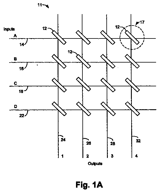
- the optical switch points may be further arranged so as to form a switching matrix. For example, when arranged in a 32 x 32 matrix, formed by 32 rows and 32 columns of optical switch points, a 32 fiber optic ribbon cable can be connected to 32 input lines and another 32 fiber optic ribbon cable can be connected to 32 output lines, the output lines intersecting the 32 input lines. Because a switch element is located at each optical switch point it is possible to switch any of the 32 input lines to any of the 32 output lines. In this manner, optical signals may be directed from one fiber optic cable onto another, resulting in a compact optical switch.
- the invention provides a system and method by which to accurately and economically test, calibrate and monitor the performance of an optical switch.
- the waveguide segments may be connected to optical fibers at the inputs and outputs.
- Input waveguides 14, 16, 18 and 22, and output waveguides 24, 26, 28 and 32 may be connected to optical fiber ribbon cable using optical fiber connectors, the waveguides being typically spaced on the order of .25 millimeters apart.
- Fig. 8 is a schematic view illustrating an alternative embodiment 90 of the first-type optical switch point 17 of Fig. 2B.
- a reflector 95 Added to first-type optical switch point 17 is a reflector 95.
- Reflector 95 is positioned so that a reflective surface thereof faces the surface of cross point switch element 12 opposite that of the surface where light traveling in input waveguide 14 is reflected onto output waveguide 28 when cross point switch element 12 is in a reflective state.
- light traveling along output waveguide segment 29 may be reflected onto input waveguide segment 15 by being reflected off the "back side" of cross point switch element 12 toward reflector 95 and off reflector 95 back onto the "back side” of cross point switch element 12 and then onto input waveguide segment 15.
- each cross point switch element 12 located at optical switch point 90 can be used to reflect two paths of light, one path on a front side of optical switch point 17 and one path on a back side of optical switch point 17.
Landscapes
- Physics & Mathematics (AREA)
- General Physics & Mathematics (AREA)
- Optics & Photonics (AREA)
- Mechanical Light Control Or Optical Switches (AREA)
- Optical Communication System (AREA)
- Use Of Switch Circuits For Exchanges And Methods Of Control Of Multiplex Exchanges (AREA)
Abstract
Description
Claims (10)
- An optical switch (70), comprising:a plurality of intersecting optical paths (14, 16, 18, 22, 24, 26, 28, 32);a plurality of cross point switch elements (12), each of said plurality of cross point switch elements (12) associated with an intersection of two of said optical paths (14, 16, 18, 22, 24, 26, 28, 32), each said cross point switch element (12) and each said intersection of two optical paths comprising an optical switch point, wherein each of said plurality of cross point switch elements (12) is arranged on a first side of said intersection of two optical paths resulting in a first-type optical switch point (17), wherein said plurality of first-type optical switch points (17) define a core matrix (11) allowing light directed at each of said first-type optical switch points (17) to be reflected when said cross point switch element (12) is in a reflective state, said core matrix (11) including a plurality of rows and a plurality of columns;a plurality of second-type optical switch points (55) forming a test row (60) and a test column (50) added to said core matrix (11), each of said plurality of second-type optical switch points (55) defined by the placement of said cross point switch element (12) on a second side of said intersection of two optical paths;a test input (56) and a test output (57) optically coupled to said test column (50) and said test row (60).
- The optical switch (70) of claim 1, wherein said plurality of second-type optical switch points (55) enable each of said plurality of first-type optical switch points (17) to be tested using said test input (56) and said test output (57).
- The optical switch (70) of claim 1, further comprising an additional column (100) and an additional row (110) of optical switch points.
- The optical switch (70) of claim 1, wherein said optical paths are waveguide segments.
- The optical switch (70) of claim 3, wherein said additional column (100) and said additional row (110) of optical switch points includes both first-type optical switch points (17) and second-type optical switch points (55).
- The optical switch (70) of claim 3, further comprising a reflector (95) in optical communication with a reverse surface of each of said plurality of first-type optical switch points (17) in said core matrix (11).
- A method for testing an optical switch point that is a member of an optical switch matrix (70), said optical switch matrix (70) comprising a plurality of intersecting optical paths (14, 16, 18, 22, 24, 26, 28, 32) and a cross point switch element (12) located at an intersection of each of said plurality of optical paths (14, 16, 18, 22, 24, 26, 28, 32), wherein said cross point switch element (12) is located on a first side of said intersection of two optical paths forming a first-type optical switch point (17), wherein a plurality of first-type optical switch points (17) are formed into a core matrix (11), said core matrix (11) having a plurality of rows and a plurality of columns, the method comprising the steps of:adding to said plurality of first-type optical switch points (17) a plurality of second-type optical switch points (55), each of said plurality of second-type optical switch points (55) formed by placing said cross point switch element (12) on a second side of said intersection of two optical paths, said plurality of second-type optical switch points (55) forming a test row (60) and a test column (50); andtesting each of said plurality of first-type optical switch points (17) using a test input (56) and a test output (57) by making reflective at least one of said first-type optical switch points (17), at least one of said second-type optical switch points (55) in said test row (60), and at least one of said second-type optical switch points (55) in said test column (50).
- The method of claim 7, further comprising the step of adding an additional column (100) and an additional row (110) of optical switch points to said core matrix (11).
- The method of claim 8, wherein said additional column (100) and said additional row (110) of optical switch points include both first-type optical switch points (17) and second-type optical switch points (55).
- A method for calibrating an optical switch point that is a member of an optical switch matrix (70), said optical switch matrix (70) comprising a plurality of intersecting optical paths (14, 16, 18, 22, 24, 26, 28, 32) and a cross point switch element (12) located at an intersection of two of said optical paths (14, 16, 18, 22, 24, 26, 28, 32), said cross point switch element (12) and said intersection of two optical paths forming an optical switch point, wherein the placement of said cross point switch element (12) on a first side of said intersection of two optical paths results in a first-type optical switch point (17) and wherein the placement of said cross point switch element on a second side of said intersection of two optical paths results in a second-type optical switch point (55), the method comprising the steps of:adding to said plurality of first-type optical switch points (17) arranged in a core matrix (11) a plurality of second-type optical switch points (55), said plurality of second-type optical switch points (55) defining a test row (60) and a test column (50);calibrating each of said plurality of first-type optical switch points (17) using a test input (56) and a test output (57) by making reflective at least one of said first-type optical switch points (17), at least one of said second-type optical switch points (55) in said test row (60), and at least one of said second-type optical switch points (55) in said test column (50); andmeasuring a reflectivity of each of said plurality of first-type optical switch points (17).
Applications Claiming Priority (2)
| Application Number | Priority Date | Filing Date | Title |
|---|---|---|---|
| US09/293,044 US6198856B1 (en) | 1999-04-16 | 1999-04-16 | Optical switch having test ports |
| US293044 | 1999-04-16 |
Publications (2)
| Publication Number | Publication Date |
|---|---|
| EP1045265A2 true EP1045265A2 (en) | 2000-10-18 |
| EP1045265A3 EP1045265A3 (en) | 2003-04-02 |
Family
ID=23127397
Family Applications (1)
| Application Number | Title | Priority Date | Filing Date |
|---|---|---|---|
| EP00106542A Withdrawn EP1045265A3 (en) | 1999-04-16 | 2000-03-27 | Optical switch having test ports |
Country Status (3)
| Country | Link |
|---|---|
| US (1) | US6198856B1 (en) |
| EP (1) | EP1045265A3 (en) |
| JP (1) | JP4448597B2 (en) |
Cited By (6)
| Publication number | Priority date | Publication date | Assignee | Title |
|---|---|---|---|---|
| EP1143285A1 (en) * | 2000-04-07 | 2001-10-10 | Nortel Networks Limited | Testing operation of a photonic matrix switch |
| EP1273942A1 (en) * | 2001-06-27 | 2003-01-08 | Agilent Technologies, Inc. (a Delaware corporation) | Optical cross-switch signal monitoring method and system therefor |
| EP1229375A3 (en) * | 2001-01-31 | 2004-01-28 | Agilent Technologies, Inc. (a Delaware corporation) | Optical cross-switch gas intrusion detector and detection method |
| WO2007090772A3 (en) * | 2006-02-03 | 2007-09-20 | Siemens Ag | Circuit and testing device |
| CN109787595A (en) * | 2018-12-29 | 2019-05-21 | 北京航天测控技术有限公司 | A kind of matrix switch and its control method |
| CN115955620A (en) * | 2023-03-07 | 2023-04-11 | 之江实验室 | Calibration method of switch unit in silicon-based optical switch chip based on Banyan network |
Families Citing this family (37)
| Publication number | Priority date | Publication date | Assignee | Title |
|---|---|---|---|---|
| US6320995B1 (en) * | 1999-08-11 | 2001-11-20 | Agilent Technologies, Inc | Loss equalization by means of port interconnectivity in a multistage optical switch |
| US6583916B2 (en) * | 1999-11-03 | 2003-06-24 | Optodot Corporation | Optical shutter assembly |
| US6798992B1 (en) * | 1999-11-10 | 2004-09-28 | Agere Systems Inc. | Method and device for optically crossconnecting optical signals using tilting mirror MEMS with drift monitoring feature |
| US6862380B2 (en) * | 2000-02-04 | 2005-03-01 | At&T Corp. | Transparent optical switch |
| US6396972B1 (en) * | 2000-02-09 | 2002-05-28 | Agilent Technologies, Inc. | Thermally actuated optical add/drop switch |
| US6473544B1 (en) * | 2000-03-03 | 2002-10-29 | Onix Microsystems, Inc. | Optical switch having equalized beam spreading in all connections |
| US6493479B1 (en) * | 2000-04-07 | 2002-12-10 | Nortel Networks Limited | Crosspoint switch protection using additional switching elements to provide alternate paths |
| TW434419B (en) * | 2000-04-24 | 2001-05-16 | Ind Tech Res Inst | Structure of optical switches of multiple mirror reflection |
| US6430334B1 (en) | 2000-04-25 | 2002-08-06 | Ball Semiconductor, Inc. | System and method for refracting and deflecting light utilizing liquid crystal bars and blocks |
| US6444976B1 (en) * | 2000-04-25 | 2002-09-03 | Ball Semiconductor, Inc. | System and method for reflecting and deflecting light utilizing spherical shaped devices |
| US6519383B1 (en) * | 2000-11-28 | 2003-02-11 | Nortel Networks Limited | Photonic switch status tester |
| US6526195B1 (en) * | 2001-01-22 | 2003-02-25 | Nortel Networks Limited | Protecting optical switches |
| US7183633B2 (en) * | 2001-03-01 | 2007-02-27 | Analog Devices Inc. | Optical cross-connect system |
| US6906511B2 (en) * | 2001-05-08 | 2005-06-14 | Analog Devices, Inc. | Magnetic position detection for micro machined optical element |
| US6470107B2 (en) | 2001-03-13 | 2002-10-22 | President And Fellows Of Harvard College | Fluidic all-optical switch |
| US6944361B2 (en) | 2001-04-13 | 2005-09-13 | Gazillion Bits, Inc. | Electrically controllable integrated optical cross-connect |
| US6714701B1 (en) * | 2001-05-29 | 2004-03-30 | Nortel Networks Limited | Optical switch using micromirrors and method of testing the same |
| US6882766B1 (en) | 2001-06-06 | 2005-04-19 | Calient Networks, Inc. | Optical switch fabric with redundancy |
| US6580847B2 (en) | 2001-06-13 | 2003-06-17 | Agilent Technologies, Inc. | Multistage photonic switch fault isolation |
| US7110633B1 (en) | 2001-08-13 | 2006-09-19 | Calient Networks, Inc. | Method and apparatus to provide alternative paths for optical protection path switch arrays |
| US6668107B2 (en) * | 2001-12-21 | 2003-12-23 | Agilent Technologies, Inc. | Method and apparatus for reducing optical insertion loss in planar lightwave circuits through dielectric perturbation optimization |
| US7532782B2 (en) * | 2002-04-18 | 2009-05-12 | Pivotal Decisions Llc | Flexible optical circuit apparatus and method |
| US6983087B1 (en) * | 2002-05-24 | 2006-01-03 | Cypress Semiconductor Corporation | Cascading optical switch multi-plane system and method |
| US7013058B1 (en) | 2002-05-24 | 2006-03-14 | Cypress Semiconductor Corporation | Optical switch cascading system and method with fixed incidence angle correction |
| US6853762B1 (en) | 2002-05-24 | 2005-02-08 | Cypress Semiconductor Corporation | Optical switch cascading system and method with variable incidence angle correction |
| US6937783B2 (en) * | 2002-06-07 | 2005-08-30 | Charles Chu | 2-D optical switch with lens mount |
| US7221819B2 (en) | 2002-08-01 | 2007-05-22 | Avago Technologies Fiber Ip (Singapore) Pte. Ltd. | Operating an optical switch at a negative pressure differential |
| JP2004077854A (en) * | 2002-08-20 | 2004-03-11 | Fujitsu Ltd | Optical switch and method of using the same |
| US6870982B1 (en) | 2002-08-23 | 2005-03-22 | Cypress Semiconductor Corporation | Cascading optical switch three dimensional switch fabric system and method |
| JP2004101944A (en) * | 2002-09-10 | 2004-04-02 | Sumitomo Electric Ind Ltd | Optical switch, light emitting device switching method, light receiving device switching method, multiplexer, demultiplexer, and optical communication system |
| US6876788B2 (en) * | 2002-09-11 | 2005-04-05 | Agilent Technologies, Inc. | Preventing hydrodynamic crosstalk in an optical switch |
| US7653272B2 (en) * | 2002-09-19 | 2010-01-26 | Avago Technologies Fiber Ip (Singapore) Pte. Ltd. | Highly parallel optical communication system with intracard and intercard communications |
| US7151868B1 (en) * | 2002-10-15 | 2006-12-19 | Finisar Corporation | Optical switch having a reflective component |
| US20050146712A1 (en) * | 2003-12-24 | 2005-07-07 | Lynx Photonics Networks Inc. | Circuit, system and method for optical switch status monitoring |
| US7676125B2 (en) * | 2006-06-19 | 2010-03-09 | Calient Networks, Inc. | Method and apparatus to provide multi-channel bulk fiber optical power detection |
| CN107678098B (en) * | 2016-08-01 | 2019-09-03 | 华为技术有限公司 | Optical Switches and Optical Switching Systems |
| US11199665B2 (en) * | 2020-01-28 | 2021-12-14 | Hewlett Packard Enterprise Development Lp | Optical device for redirecting optical signals |
Family Cites Families (5)
| Publication number | Priority date | Publication date | Assignee | Title |
|---|---|---|---|---|
| US4121884A (en) | 1976-10-08 | 1978-10-24 | International Standard Electric Corporation | Optical fiber switch |
| US5732168A (en) * | 1995-10-31 | 1998-03-24 | Hewlett Packard Company | Thermal optical switches for light |
| US5699462A (en) | 1996-06-14 | 1997-12-16 | Hewlett-Packard Company | Total internal reflection optical switches employing thermal activation |
| US5982554A (en) * | 1997-12-31 | 1999-11-09 | At&T Corp | Bridging apparatus and method for an optical crossconnect device |
| US6055344A (en) * | 1998-02-18 | 2000-04-25 | Hewlett-Packard Company | Fabrication of a total internal reflection optical switch with vertical fluid fill-holes |
-
1999
- 1999-04-16 US US09/293,044 patent/US6198856B1/en not_active Expired - Lifetime
-
2000
- 2000-03-27 EP EP00106542A patent/EP1045265A3/en not_active Withdrawn
- 2000-04-14 JP JP2000113365A patent/JP4448597B2/en not_active Expired - Fee Related
Cited By (9)
| Publication number | Priority date | Publication date | Assignee | Title |
|---|---|---|---|---|
| EP1143285A1 (en) * | 2000-04-07 | 2001-10-10 | Nortel Networks Limited | Testing operation of a photonic matrix switch |
| US6574384B1 (en) | 2000-04-07 | 2003-06-03 | Nortel Networks Limited | Testing operation of a photonic switch |
| EP1229375A3 (en) * | 2001-01-31 | 2004-01-28 | Agilent Technologies, Inc. (a Delaware corporation) | Optical cross-switch gas intrusion detector and detection method |
| EP1273942A1 (en) * | 2001-06-27 | 2003-01-08 | Agilent Technologies, Inc. (a Delaware corporation) | Optical cross-switch signal monitoring method and system therefor |
| WO2007090772A3 (en) * | 2006-02-03 | 2007-09-20 | Siemens Ag | Circuit and testing device |
| CN109787595A (en) * | 2018-12-29 | 2019-05-21 | 北京航天测控技术有限公司 | A kind of matrix switch and its control method |
| CN109787595B (en) * | 2018-12-29 | 2022-11-25 | 北京航天测控技术有限公司 | Matrix switch and control method thereof |
| CN115955620A (en) * | 2023-03-07 | 2023-04-11 | 之江实验室 | Calibration method of switch unit in silicon-based optical switch chip based on Banyan network |
| CN115955620B (en) * | 2023-03-07 | 2023-06-23 | 之江实验室 | Calibration method of switching unit in silicon-based optical switching chip based on Banyan network |
Also Published As
| Publication number | Publication date |
|---|---|
| JP2000321512A (en) | 2000-11-24 |
| JP4448597B2 (en) | 2010-04-14 |
| US6198856B1 (en) | 2001-03-06 |
| EP1045265A3 (en) | 2003-04-02 |
Similar Documents
| Publication | Publication Date | Title |
|---|---|---|
| US6198856B1 (en) | Optical switch having test ports | |
| US6160928A (en) | Fault tolerant optical switch | |
| US6999677B2 (en) | Protection switching arrangement for an optical switching system | |
| US20050213978A1 (en) | Wavelength demultiplexing unit | |
| CA2655746A1 (en) | Optical communication system | |
| CN102645705A (en) | Wavelength division multiplexer (WDM), optical switch device and optical switch control method | |
| US20040105613A1 (en) | Optoelectronic module with integrated loop-back capability | |
| JP4819246B2 (en) | Optical add / drop switch | |
| US6731834B2 (en) | System and method to calibrate an optical cross-connect | |
| KR101165715B1 (en) | Optical communication device haiving digital optical switch | |
| EP1143760A2 (en) | Crosspoint switch protection | |
| US6928244B1 (en) | System and method of wavelength add/drop multiplexing having client configurability | |
| US6519383B1 (en) | Photonic switch status tester | |
| JP2721211B2 (en) | Branch optical line loss distribution measurement device | |
| US5995687A (en) | Circuit for testing an optical communication system | |
| US6574384B1 (en) | Testing operation of a photonic switch | |
| KR20130006353A (en) | Optical data transmission system | |
| JP4103999B2 (en) | Optical line loss measuring method and measuring apparatus | |
| KR100917562B1 (en) | Ray Management System | |
| JP2005091160A (en) | Optical line monitoring device | |
| JP4173967B2 (en) | Optical fiber loss measuring method and measuring apparatus | |
| US7162116B1 (en) | Depopulated switchable micro electro-mechanical systems (MEMS) based module for photonic fabric verification and protection | |
| CN101802668A (en) | Optical switch matrix | |
| JPH03296334A (en) | Optical communication system | |
| JP2006119079A (en) | Fault detection system for passive branching optical fiber line |
Legal Events
| Date | Code | Title | Description |
|---|---|---|---|
| PUAI | Public reference made under article 153(3) epc to a published international application that has entered the european phase |
Free format text: ORIGINAL CODE: 0009012 |
|
| AK | Designated contracting states |
Kind code of ref document: A2 Designated state(s): AT BE CH CY DE DK ES FI FR GB GR IE IT LI LU MC NL PT SE |
|
| AX | Request for extension of the european patent |
Free format text: AL;LT;LV;MK;RO;SI |
|
| RAP1 | Party data changed (applicant data changed or rights of an application transferred) |
Owner name: AGILENT TECHNOLOGIES INC. |
|
| RAP1 | Party data changed (applicant data changed or rights of an application transferred) |
Owner name: AGILENT TECHNOLOGIES INC. A DELAWARE CORPORATION |
|
| RAP1 | Party data changed (applicant data changed or rights of an application transferred) |
Owner name: AGILENT TECHNOLOGIES, INC. (A DELAWARE CORPORATION |
|
| PUAL | Search report despatched |
Free format text: ORIGINAL CODE: 0009013 |
|
| RIC1 | Information provided on ipc code assigned before grant |
Ipc: 7H 04Q 11/00 B Ipc: 7G 02F 1/313 B Ipc: 7G 02B 6/35 B Ipc: 7G 02B 6/28 A |
|
| AK | Designated contracting states |
Kind code of ref document: A3 Designated state(s): AT BE CH CY DE DK ES FI FR GB GR IE IT LI LU MC NL PT SE Designated state(s): AT BE CH CY DE DK ES FI FR GB GR IE IT LI LU MC NL PT SE |
|
| AX | Request for extension of the european patent |
Extension state: AL LT LV MK RO SI |
|
| 17P | Request for examination filed |
Effective date: 20030327 |
|
| AKX | Designation fees paid |
Designated state(s): DE FR GB IT |
|
| STAA | Information on the status of an ep patent application or granted ep patent |
Free format text: STATUS: THE APPLICATION HAS BEEN WITHDRAWN |
|
| 18W | Application withdrawn |
Effective date: 20040630 |