EP1043771A2 - Resin sealed electronic device and method of fabricating the same and ignition coil for internal combustion engine using the same - Google Patents
Resin sealed electronic device and method of fabricating the same and ignition coil for internal combustion engine using the same Download PDFInfo
- Publication number
- EP1043771A2 EP1043771A2 EP00107061A EP00107061A EP1043771A2 EP 1043771 A2 EP1043771 A2 EP 1043771A2 EP 00107061 A EP00107061 A EP 00107061A EP 00107061 A EP00107061 A EP 00107061A EP 1043771 A2 EP1043771 A2 EP 1043771A2
- Authority
- EP
- European Patent Office
- Prior art keywords
- resin
- transfer molding
- electronic device
- flip chip
- circuit board
- Prior art date
- Legal status (The legal status is an assumption and is not a legal conclusion. Google has not performed a legal analysis and makes no representation as to the accuracy of the status listed.)
- Granted
Links
Images






Classifications
-
- H—ELECTRICITY
- H10—SEMICONDUCTOR DEVICES; ELECTRIC SOLID-STATE DEVICES NOT OTHERWISE PROVIDED FOR
- H10W—GENERIC PACKAGES, INTERCONNECTIONS, CONNECTORS OR OTHER CONSTRUCTIONAL DETAILS OF DEVICES COVERED BY CLASS H10
- H10W74/00—Encapsulations, e.g. protective coatings
- H10W74/40—Encapsulations, e.g. protective coatings characterised by their materials
- H10W74/47—Encapsulations, e.g. protective coatings characterised by their materials comprising organic materials, e.g. plastics or resins
- H10W74/473—Encapsulations, e.g. protective coatings characterised by their materials comprising organic materials, e.g. plastics or resins containing a filler
-
- H—ELECTRICITY
- H10—SEMICONDUCTOR DEVICES; ELECTRIC SOLID-STATE DEVICES NOT OTHERWISE PROVIDED FOR
- H10W—GENERIC PACKAGES, INTERCONNECTIONS, CONNECTORS OR OTHER CONSTRUCTIONAL DETAILS OF DEVICES COVERED BY CLASS H10
- H10W74/00—Encapsulations, e.g. protective coatings
- H10W74/01—Manufacture or treatment
- H10W74/012—Manufacture or treatment of encapsulations on active surfaces of flip-chip devices, e.g. forming underfills
-
- H—ELECTRICITY
- H10—SEMICONDUCTOR DEVICES; ELECTRIC SOLID-STATE DEVICES NOT OTHERWISE PROVIDED FOR
- H10W—GENERIC PACKAGES, INTERCONNECTIONS, CONNECTORS OR OTHER CONSTRUCTIONAL DETAILS OF DEVICES COVERED BY CLASS H10
- H10W74/00—Encapsulations, e.g. protective coatings
- H10W74/10—Encapsulations, e.g. protective coatings characterised by their shape or disposition
- H10W74/15—Encapsulations, e.g. protective coatings characterised by their shape or disposition on active surfaces of flip-chip devices, e.g. underfills
-
- H—ELECTRICITY
- H10—SEMICONDUCTOR DEVICES; ELECTRIC SOLID-STATE DEVICES NOT OTHERWISE PROVIDED FOR
- H10W—GENERIC PACKAGES, INTERCONNECTIONS, CONNECTORS OR OTHER CONSTRUCTIONAL DETAILS OF DEVICES COVERED BY CLASS H10
- H10W72/00—Interconnections or connectors in packages
- H10W72/851—Dispositions of multiple connectors or interconnections
- H10W72/853—On the same surface
- H10W72/856—Bump connectors and die-attach connectors
-
- H—ELECTRICITY
- H10—SEMICONDUCTOR DEVICES; ELECTRIC SOLID-STATE DEVICES NOT OTHERWISE PROVIDED FOR
- H10W—GENERIC PACKAGES, INTERCONNECTIONS, CONNECTORS OR OTHER CONSTRUCTIONAL DETAILS OF DEVICES COVERED BY CLASS H10
- H10W90/00—Package configurations
- H10W90/701—Package configurations characterised by the relative positions of pads or connectors relative to package parts
- H10W90/721—Package configurations characterised by the relative positions of pads or connectors relative to package parts of bump connectors
- H10W90/724—Package configurations characterised by the relative positions of pads or connectors relative to package parts of bump connectors between a chip and a stacked insulating package substrate, interposer or RDL
-
- H—ELECTRICITY
- H10—SEMICONDUCTOR DEVICES; ELECTRIC SOLID-STATE DEVICES NOT OTHERWISE PROVIDED FOR
- H10W—GENERIC PACKAGES, INTERCONNECTIONS, CONNECTORS OR OTHER CONSTRUCTIONAL DETAILS OF DEVICES COVERED BY CLASS H10
- H10W90/00—Package configurations
- H10W90/701—Package configurations characterised by the relative positions of pads or connectors relative to package parts
- H10W90/731—Package configurations characterised by the relative positions of pads or connectors relative to package parts of die-attach connectors
- H10W90/734—Package configurations characterised by the relative positions of pads or connectors relative to package parts of die-attach connectors between a chip and a stacked insulating package substrate, interposer or RDL
Definitions
- the present invention provides a resin sealed electronic device which mounts a flip chip type monolithic IC on a hybrid circuit board through bumps, and is packaged with a transfer molding resin, wherein the resin sealed electronic device is integrated in a unit including the hybrid circuit board mounting the flip chip type monolithic IC through transfer molding with the transfer molding resin, and a gap between the flip chip type monolithic IC and the hybrid circuit board is filled with the transfer molding resin flown around at transfer molding excluding voids or including voids.
- the present invention further provides a method of fabricating a resin sealed electronic device, wherein the epoxy resin contains silicone of 1 to 8 %.
- the present invention further provides a method of fabricating a resin sealed electronic device, wherein the filler is composed of cubicle molten silica particles, spherical molten silica particles or a mixture of the molten silica particles.
- Wettability of the solder can be secured by setting the content of silver in the solder of silver/tin group to 1 to 5 %.
- the semiconductor element and the hybrid circuit board can be prevented from being damaged by sharp edges in corners of the particles.
- the semiconductor element and the hybrid circuit board can be prevented from being damaged best when the cubicle molten silica particles are solely used.
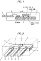
- Fig. 1 is a vertical cross-sectional view showing the construction of an embodiment of a resin sealed electronic device in accordance with the present invention.
- a flip chip type monolithic (hereinafter, referred to as "flip chip”) IC 1 is mounted on a hybrid IC board or a glass-epoxy board 3, which has conductor wires and resistors formed on a substrate of ceramic group, through solder bumps 2.
- the conductor wiring is not shown in this cross-sectional view.
- a pad 7 for wire bonding is soldered on the hybrid circuit board 3 through solder 8, and connected to an external input/output terminal portion 5 with an aluminum wire 6.
- An electric function is constructed by supplying electric power to the circuit, and by inputting and outputting signals through the external input/output terminal portions 5, and by performing desired processing of the signals using the hybrid circuit board 3 including the flip chip IC 1.
- the reference character 4' in the figure indicates the transfer molding resin flowing around into the gap.
- the high temperature durability of the resin sealed electronic device can be secured by employing the solder of tin/lead group for the solder used.
- the solder of tin/silver group for the solder, the lead-free resin sealed electronic device can be attained.
- the flip chip IC 1 is soldered onto a conductor wiring portion 9 on the hybrid circuit board 3 through the solder bumps 2.
- the surface of the conductor wiring portion 9 other than a portion to be soldered is protected with coating glass 10 or the like.
- the solder bump 2 portion under the flip chip IC 1 is filled with the transfer molding resin 4 containing a molten filler 11 composed of cubicle particles, spherical particles or a mixture of them which has been injected under a transfer molding pressure.
- Fig. 4 is an enlarged cross-sectional view showing a flip chip portion of a resin sealed electronic device in which a void remains.
- the thickness of the resin around the flip chip 1 is largely different from the thickness of the resin under the bump 2 portion, the void sometimes remains under the flip chip IC 1.
- the transfer molding resin 4 covers the whole flip chip IC in the initial stage of molding because the thickness in the periphery of the flip chip IC 1, and then enters under the solder bump 2 portion of the flip chip IC. Therefore, the air remaining under the flip chip IC 1 becomes a void and remains near the central portion under the flip chip IC. When the flip chip is small, the size of the remaining void is near the value that the air under the flip chip IC is compressed with the molding pressure.
- the transfer molding resin covers the whole flip chip IC because the gap between the flip chip IC and the board of the bump portion is narrow, and then enters under the chip as shown by the arrows in the figure to produce the void 12.
- the stress effect due to the produced void is negligible.
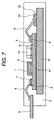
- Fig. 7 is a view showing a further embodiment of a complex power system resin sealed electronic device in accordance with the present invention.
- a resin sealed type electronic device is formed by transfer-molding the hybrid circuit board 3, the overall surface or one side surface in the side of mounting the hybrid circuit board 3 of the base portion 16 mounting the power system semiconductor element and part of the external input and output terminals 5 with a transfer molding resin 4 containing a filler (not shown in the figure).
- the present embodiment it is possible to construct a complex power system resin sealed type electronic device reducing the thermal stress exerting on the solder bump 2 portion and having the high reliability by stipulating the linear expansion coefficient of the molding resin used and the size of the filler particles without using the under filler described above and by applying the transfer molding commonly used in packaging of semiconductor products to the hybrid circuit including the flip chip type IC and the power system semiconductor element.
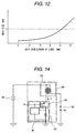
- Fig. 11 is a chart showing the effect that in the resin sealed type electronic device using only the transfer molding resin without using the under filler material, the strain caused in the solder bumps is reduced compared to the conventional electronic device. Since the solder bumps are directly restricted by the integrated transfer molding resin, control of the thermal expansion state is uniquely performed and accordingly the strain caused in the solder bumps is decreased by the amount.
- the present invention is effective when the chip size of the flip chip is smaller than 5mm ⁇ 5mm.
- the value of the void size under the chip is varied depending on the required durability.
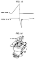
- Fig. 15 shows the operation waveform of Fig. 14.
- a secondary voltage V2 is generated in the secondary side of the coil when the primary current I1 is broken.
- the primary current is broken generally in 6 to 8 A and at that time the generated secondary voltage becomes 20 to 30 kV.
- the coil 31 in the present embodiment is a cylindrical coil
- the coils 31 are inserted into and attached to the plug holes of the engine.
- the present embodiment of the resin sealed type electronic device is contained into the coil 31 as described above, it is particularly necessary to take the thermal stress into consideration because the coil is directly attached to the engine.
- the resin sealed type electronic device is transfer-molded with the transfer molding resin in a unit including the hybrid circuit board mounting the flip chip IC
- the structure formed through the transfer molding becomes a unit and the effect of thermal stress can be decreased because there is no need to use the conventionally used under filler material, the stress exerting on the solder bump can be reduced, and the fabricating process is simplified.
Landscapes
- Structures Or Materials For Encapsulating Or Coating Semiconductor Devices Or Solid State Devices (AREA)
- Encapsulation Of And Coatings For Semiconductor Or Solid State Devices (AREA)
Abstract
Description
Claims (16)
- A resin sealed electronic device which mounts a flip chip type monolithic IC (1) on a hybrid circuit board (3) through bumps (2), and is packaged with a thermosetting resin (4) through transfer molding, whereinsaid thermosetting resin (4) used for the transfer molding (hereinafter, referred to as "transfer molding resin") has a linear expansion coefficient of 3x10⁻⁶ to 17X10-6 and contains a filler having a particle size smaller than a height of the bump by more than 10 µm, andsaid resin sealed electronic device is integrated in a unit including the hybrid circuit board (3) mounting the flip chip type monolithic IC (1) through transfer molding with said transfer molding resin (4).
- A resin sealed electronic device according to claim 1, whereinsize of said filler is smaller than 75 µm.
- A resin sealed electronic device which mounts a flip chip type monolithic IC (1) on a hybrid circuit board (3) through bumps (2), and is packaged with a transfer molding resin (4), whereinsaid resin sealed electronic device is integrated in a unit including the hybrid circuit board (3) mounting the flip chip type monolithic IC (1) through transfer molding with said transfer molding resin (4), andsaid bump (2) is restrained from moving by the transfer molding resin (4) flowing around at transfer-molding.
- A resin sealed electronic device which mounts a flip chip type monolithic IC (1) on a hybrid circuit board (3) through bumps (2), and is packaged with a transfer molding resin (4), whereinsaid resin sealed electronic device is integrated in a unit including the hybrid circuit board (3) mounting the flip chip type monolithic IC (1) through transfer molding with said transfer molding resin (4); anda gap between said flip chip type monolithic IC (1) and said hybrid circuit board (3) is filled with said transfer molding resin (4) flown around at transfer molding excluding voids or including voids.
- A resin sealed electronic device according to any one of claim 1 to claim 4, whereinsaid bump (2) is soldered to a conductor wire on the hybrid circuit board (3), and surfaces of said bump (2) except for a surface to be soldered are coated, and said transfer molding resin (4) is thermally set on said coated surfaces.
- A resin sealed electronic device according to any one of claim 1 to claim 4, whereinsaid transfer molding resin (4) uses an epoxy resin.
- A method of fabricating a resin sealed electronic device which mounts a flip chip type monolithic IC (1) on a hybrid circuit board (3) through bumps (2), and is packaged with a transfer molding resin, the method comprising the steps of:performing molding using said transfer molding resin (4) having a linear expansion coefficient of 3X10⁻⁶ to 17X10-6 and containing a filler having a particle size smaller than a height of the bump by more than 10 µm; andexerting a transfer molding pressure at said molding so that said transfer molding resin is let flow around between said flip chip type monolithic IC (1) and said hybrid circuit board (3).
- A method of fabricating a resin sealed electronic device according to claim 7, whereinsaid transfer molding resin (4) uses an epoxy resin and said epoxy resin is octo-cresol novolak type epoxy resin, anda glass transition point temperature of said epoxy resin is higher than 150 °C.
- A method of fabricating a resin sealed electronic device according to claim 8, whereinsaid epoxy resin contains silicone of 1 to 8 %.
- A method of fabricating a resin sealed electronic device according to claim 7, whereinsaid filler is composed of cubicle molten silica particles, spherical molten silica particles or a mixture of the molten silica particles.
- A resin sealed electronic device according to any one of claim 1 to claim 4, whereinsaid hybrid circuit board (3) is mounted on a lead frame of copper group; a power system semiconductor element being mounted at a position on said lead frame other than the board mounting portion using a solder or an electric conductive adhesive;a bonding pad portion provided on said circuit board being connected to a bonding pad portion of the semiconductor element by wire bonding; and an external output terminal portion formed in said lead frame being connected to said circuit board similarly by wire bonding.
- A resin sealed electronic device according to any one of claim 1 to claim 4, whereina ceramic substrate of alumina group having a conductor of silver/platinum group or a conductor of copper group is used for said hybrid circuit board; anda high temperature solder of lead/tin group is used for the solder in the bump portion of the flip chip and the solder used for mounting discrete parts mounted on the board.
- A resin sealed electronic device according to any one of claim 1 to claim 4, whereina ceramic substrate of alumina group having a conductor of silver/platinum group or a conductor of copper group is used for said hybrid circuit board; anda high temperature solder of silver/tin group is used for the solder in the bump portion of the flip chip and similarly the solder used for mounting discrete parts mounted on the board.
- A resin sealed electronic device according to any one of claim 1 to claim 4, whereina high heat resistance glass-epoxy substrate having a linear expansion coefficient smaller than 17X10-6 is used for the hybrid circuit board, anda high temperature solder of silver/tin group is used for the solder in the bump portion of the flip chip and similarly the solder used for mounting discrete parts mounted on the board.
- A resin sealed electronic device according to any one of claim 13 to claim 14, whereinsaid solder of silver/tin group used contains silver of 1 to 5 %.
- An internal combustion engine ignition coil device comprising a resin sealed electronic device which mounts a flip chip type monolithic IC (1) on a hybrid circuit board (3) through bumps (2), and is packaged with a transfer molding resin, wherein said resin sealed electronic device comprises a flip chip type monolithic IC (1) having a size smaller than 5 mm X 5 mm;a molding body integrated in a unit including the hybrid circuit board (3) mounting the flip chip type monolithic IC (1) through transfer molding with the transfer molding resin (4); anda structure that said molding body is embedded into the coil main body with a molding resin having a thermal expansion coefficient larger than a thermal expansion coefficient of said transfer molding resin, and a transfer molding resin portion composing said molding body shows a continuous uniform stress diagram including the transfer molding resin portion between the flip chip type monolithic IC (1) and the hybrid circuit board (3).
Applications Claiming Priority (2)
| Application Number | Priority Date | Filing Date | Title |
|---|---|---|---|
| JP9908899 | 1999-04-06 | ||
| JP11099088A JP2000294692A (en) | 1999-04-06 | 1999-04-06 | Resin-sealed electronic device, method of manufacturing the same, and ignition coil device for internal combustion engine using the same |
Publications (3)
| Publication Number | Publication Date |
|---|---|
| EP1043771A2 true EP1043771A2 (en) | 2000-10-11 |
| EP1043771A3 EP1043771A3 (en) | 2002-08-14 |
| EP1043771B1 EP1043771B1 (en) | 2006-12-06 |
Family
ID=14238155
Family Applications (1)
| Application Number | Title | Priority Date | Filing Date |
|---|---|---|---|
| EP00107061A Expired - Lifetime EP1043771B1 (en) | 1999-04-06 | 2000-04-04 | Method of fabricating a resin sealed electronic device |
Country Status (4)
| Country | Link |
|---|---|
| US (1) | US6321734B1 (en) |
| EP (1) | EP1043771B1 (en) |
| JP (1) | JP2000294692A (en) |
| DE (1) | DE60032192T2 (en) |
Cited By (3)
| Publication number | Priority date | Publication date | Assignee | Title |
|---|---|---|---|---|
| EP1075025A3 (en) * | 1999-08-04 | 2003-12-17 | Hitachi, Ltd. | Electronic device and method of fabricating the same |
| US6919643B2 (en) | 2001-11-27 | 2005-07-19 | Koninklijke Philips Electronics N.V. | Multi-chip module semiconductor devices |
| EP1353066B1 (en) * | 2002-04-12 | 2009-10-14 | Diamond Electric MFG. Co., Ltd. | Ignition device for internal combustion engine |
Families Citing this family (36)
| Publication number | Priority date | Publication date | Assignee | Title |
|---|---|---|---|---|
| JP2001313314A (en) * | 2000-04-28 | 2001-11-09 | Sony Corp | Semiconductor device using bump, method of manufacturing the same, and method of forming bump |
| US6603191B2 (en) * | 2000-05-18 | 2003-08-05 | Casio Computer Co., Ltd. | Semiconductor device and method of manufacturing the same |
| US6632704B2 (en) * | 2000-12-19 | 2003-10-14 | Intel Corporation | Molded flip chip package |
| JP4614586B2 (en) * | 2001-06-28 | 2011-01-19 | 三洋電機株式会社 | Method for manufacturing hybrid integrated circuit device |
| TW585015B (en) * | 2001-06-28 | 2004-04-21 | Sanyo Electric Co | Hybrid integrated circuit device and method for manufacturing same |
| JP4614584B2 (en) * | 2001-06-28 | 2011-01-19 | 三洋電機株式会社 | Hybrid integrated circuit device and manufacturing method thereof |
| KR20030049284A (en) * | 2001-12-14 | 2003-06-25 | 삼성전기주식회사 | Package substrate for flip chip bonding |
| AU2003230738A1 (en) * | 2002-03-26 | 2003-10-13 | California Institute Of Technology | Active-loop, spatially-combined amplifier |
| US7390845B2 (en) * | 2002-07-26 | 2008-06-24 | Illinois Tool Works Inc | Sealing system and process therefor |
| US6758200B2 (en) * | 2002-08-06 | 2004-07-06 | Delphi Technologies, Inc. | Ignition coil driver chip on printed circuit board for plughole coil housing |
| JP2004260135A (en) * | 2003-02-06 | 2004-09-16 | Sanyo Electric Co Ltd | Semiconductor integrated device and method of manufacturing the same |
| DE10340438B4 (en) * | 2003-09-02 | 2005-08-04 | Epcos Ag | Transmitter module with improved heat dissipation |
| JP2005162846A (en) * | 2003-12-02 | 2005-06-23 | Nitto Denko Corp | Resin composition for sealing semiconductor and semiconductor device using the same |
| DE102004031889B4 (en) * | 2004-06-30 | 2012-07-12 | Infineon Technologies Ag | Semiconductor component with a housing and a semi-embedded in a plastic housing material semiconductor chip and method for producing the same |
| US7816772B2 (en) * | 2007-03-29 | 2010-10-19 | Allegro Microsystems, Inc. | Methods and apparatus for multi-stage molding of integrated circuit package |
| JP2011009604A (en) * | 2009-06-29 | 2011-01-13 | Renesas Electronics Corp | Semiconductor device, and method of manufacturing the same |
| JP2011100718A (en) * | 2009-10-05 | 2011-05-19 | Yazaki Corp | Connector |
| US8629539B2 (en) | 2012-01-16 | 2014-01-14 | Allegro Microsystems, Llc | Methods and apparatus for magnetic sensor having non-conductive die paddle |
| US10234513B2 (en) | 2012-03-20 | 2019-03-19 | Allegro Microsystems, Llc | Magnetic field sensor integrated circuit with integral ferromagnetic material |
| US9494660B2 (en) | 2012-03-20 | 2016-11-15 | Allegro Microsystems, Llc | Integrated circuit package having a split lead frame |
| US9812588B2 (en) | 2012-03-20 | 2017-11-07 | Allegro Microsystems, Llc | Magnetic field sensor integrated circuit with integral ferromagnetic material |
| US9666788B2 (en) | 2012-03-20 | 2017-05-30 | Allegro Microsystems, Llc | Integrated circuit package having a split lead frame |
| US9226428B2 (en) * | 2012-06-28 | 2015-12-29 | Intel Corporation | High heat capacity electronic components and methods for fabricating |
| JP6012531B2 (en) * | 2013-04-02 | 2016-10-25 | 三菱電機株式会社 | Semiconductor device |
| US9411025B2 (en) | 2013-04-26 | 2016-08-09 | Allegro Microsystems, Llc | Integrated circuit package having a split lead frame and a magnet |
| KR101933277B1 (en) * | 2016-08-30 | 2018-12-27 | 삼성에스디아이 주식회사 | Film-type semiconductor encapsulation member, semiconductor package prepared by using the same and method for manufacturing thereof |
| WO2019005153A1 (en) * | 2017-06-30 | 2019-01-03 | Intel Corporation | Semiconductor package having nonspherical filler particles |
| JP6890520B2 (en) * | 2017-10-04 | 2021-06-18 | 三菱電機株式会社 | Power semiconductor device |
| US10446414B2 (en) * | 2017-12-22 | 2019-10-15 | Texas Instruments Incorporated | Semiconductor package with filler particles in a mold compound |
| IT201800005299A1 (en) | 2018-05-11 | 2019-11-11 | BICYCLE COMPONENT EQUIPPED WITH STRESS / DEFORMATION SENSOR COMPENSATED FOR TEMPERATURE | |
| IT201800005294A1 (en) * | 2018-05-11 | 2019-11-11 | COMPONENT OF BICYCLE IN COMPOSITE MATERIAL AND RELATED MANUFACTURING PROCESS | |
| CA3042547A1 (en) | 2018-05-11 | 2019-11-11 | Campagnolo S.R.L. | Bicycle crankarm provided with electric/electronic system |
| IT201800005302A1 (en) | 2018-05-11 | 2019-11-11 | TRANSMISSION SIDE BICYCLE CRANK, EQUIPPED WITH STRESS / DEFORMATION DETECTOR FOR A TORQUE OR POWER METER, AS WELL AS RELATED METHODS | |
| IT201800005297A1 (en) | 2018-05-11 | 2019-11-11 | BICYCLE CRANK AND RELATIVE CRANKSET | |
| US10921391B2 (en) | 2018-08-06 | 2021-02-16 | Allegro Microsystems, Llc | Magnetic field sensor with spacer |
| US10991644B2 (en) | 2019-08-22 | 2021-04-27 | Allegro Microsystems, Llc | Integrated circuit package having a low profile |
Family Cites Families (21)
| Publication number | Priority date | Publication date | Assignee | Title |
|---|---|---|---|---|
| US3737986A (en) * | 1971-11-26 | 1973-06-12 | Western Electric Co | Explosive bonding of workpieces |
| JP2869964B2 (en) * | 1991-02-08 | 1999-03-10 | サンケン電気株式会社 | Circuit board device |
| CA2066497A1 (en) * | 1991-05-01 | 1992-11-02 | Michael K. Gallagher | Epoxy molding composition for surface mount applications |
| US5557066A (en) * | 1993-04-30 | 1996-09-17 | Lsi Logic Corporation | Molding compounds having a controlled thermal coefficient of expansion, and their uses in packaging electronic devices |
| US5508611A (en) * | 1994-04-25 | 1996-04-16 | General Motors Corporation | Ultrathin magnetoresistive sensor package |
| US6111378A (en) * | 1995-04-28 | 2000-08-29 | Ut Automotive Dearborn, Inc. | Window wiper motor system for an automotive vehicle |
| US5654081A (en) * | 1995-07-05 | 1997-08-05 | Ford Motor Company | Integrated circuit assembly with polymeric underfill body |
| IT1275591B1 (en) * | 1995-07-21 | 1997-08-06 | Gkn Birfield Ag | DIFFERENTIAL WITH LOW LOCKING VALUE |
| JPH09246300A (en) | 1996-03-12 | 1997-09-19 | Denso Corp | Method for manufacturing semiconductor device |
| US6130602A (en) * | 1996-05-13 | 2000-10-10 | Micron Technology, Inc. | Radio frequency data communications device |
| DE69705178T2 (en) * | 1996-08-31 | 2001-09-20 | Toyo Denso K.K., Tokio/Tokyo | Ignition coil device for internal combustion engines |
| JP3384259B2 (en) | 1996-09-26 | 2003-03-10 | 株式会社デンソー | Resin encapsulated semiconductor device |
| JPH10135377A (en) * | 1996-11-01 | 1998-05-22 | Hitachi Ltd | Mold type semiconductor device |
| US5981312A (en) * | 1997-06-27 | 1999-11-09 | International Business Machines Corporation | Method for injection molded flip chip encapsulation |
| DE69811296D1 (en) * | 1997-07-11 | 2003-03-20 | Bosch Gmbh Robert | Increased adhesion of the underside coating of flip chips |
| JPH1135797A (en) * | 1997-07-15 | 1999-02-09 | Matsushita Electric Works Ltd | Epoxy resin composition for sealing semiconductor, and semiconductor device |
| JPH11111543A (en) * | 1997-10-07 | 1999-04-23 | Mitsubishi Electric Corp | Ignition coil device for internal combustion engine |
| DE69934153T2 (en) * | 1998-02-02 | 2007-09-20 | Shin-Etsu Chemical Co., Ltd. | Method for mounting flip-chip semiconductor devices |
| US6085859A (en) * | 1998-05-01 | 2000-07-11 | Alderson; Mark L. | Race car |
| JP2000031343A (en) * | 1998-07-09 | 2000-01-28 | Texas Instr Japan Ltd | Semiconductor device |
| JP3512657B2 (en) * | 1998-12-22 | 2004-03-31 | シャープ株式会社 | Semiconductor device |
-
1999
- 1999-04-06 JP JP11099088A patent/JP2000294692A/en active Pending
-
2000
- 2000-04-04 DE DE60032192T patent/DE60032192T2/en not_active Expired - Fee Related
- 2000-04-04 EP EP00107061A patent/EP1043771B1/en not_active Expired - Lifetime
- 2000-04-06 US US09/544,555 patent/US6321734B1/en not_active Expired - Fee Related
Cited By (3)
| Publication number | Priority date | Publication date | Assignee | Title |
|---|---|---|---|---|
| EP1075025A3 (en) * | 1999-08-04 | 2003-12-17 | Hitachi, Ltd. | Electronic device and method of fabricating the same |
| US6919643B2 (en) | 2001-11-27 | 2005-07-19 | Koninklijke Philips Electronics N.V. | Multi-chip module semiconductor devices |
| EP1353066B1 (en) * | 2002-04-12 | 2009-10-14 | Diamond Electric MFG. Co., Ltd. | Ignition device for internal combustion engine |
Also Published As
| Publication number | Publication date |
|---|---|
| EP1043771B1 (en) | 2006-12-06 |
| DE60032192D1 (en) | 2007-01-18 |
| JP2000294692A (en) | 2000-10-20 |
| EP1043771A3 (en) | 2002-08-14 |
| US6321734B1 (en) | 2001-11-27 |
| DE60032192T2 (en) | 2008-02-21 |
Similar Documents
| Publication | Publication Date | Title |
|---|---|---|
| EP1043771B1 (en) | Method of fabricating a resin sealed electronic device | |
| EP0645805B1 (en) | Method for mounting a semiconductor device on a circuit board, and a circuit board with a semiconductor device mounted thereon | |
| JP3884354B2 (en) | Electrical / electronic module with integrated molded structure of connector and electronic component | |
| US6175159B1 (en) | Semiconductor package | |
| US5883430A (en) | Thermally enhanced flip chip package | |
| US5677575A (en) | Semiconductor package having semiconductor chip mounted on board in face-down relation | |
| US6257215B1 (en) | Resin-sealed electronic apparatus for use in internal combustion engines | |
| US5994168A (en) | Method of manufacturing semiconductor device | |
| JP2012524987A (en) | Encapsulated circuit device for a substrate with an absorption layer and method for manufacturing the circuit device | |
| US6467139B1 (en) | Mounting structure and mounting method for surface acoustic wave element | |
| US6484708B2 (en) | Resin sealed electronic device | |
| US6037656A (en) | Semiconductor integrated circuit device having short signal paths to terminals and process of fabrication thereof | |
| US6758200B2 (en) | Ignition coil driver chip on printed circuit board for plughole coil housing | |
| US6890796B1 (en) | Method of manufacturing a semiconductor package having semiconductor decice mounted thereon and elongate opening through which electodes and patterns are connected | |
| JP3666576B2 (en) | Multilayer module and manufacturing method thereof | |
| CN116913864B (en) | High-reliability integrated circuit packaging structure with small junction temperature tolerance and packaging method | |
| JP3975596B2 (en) | Hybrid integrated circuit device | |
| JP2904154B2 (en) | Electronic circuit device including semiconductor element | |
| JPH1126654A (en) | Resin-sealed semiconductor device and method of manufacturing the same | |
| JP3147157B2 (en) | Electronic circuit device including semiconductor element | |
| JP2004165525A (en) | Semiconductor device and manufacturing method thereof | |
| JP2972112B2 (en) | Power semiconductor device | |
| JP2834017B2 (en) | Semiconductor device and manufacturing method thereof | |
| JP2637684B2 (en) | Semiconductor device sealing method | |
| JP2637684C (en) |
Legal Events
| Date | Code | Title | Description |
|---|---|---|---|
| PUAI | Public reference made under article 153(3) epc to a published international application that has entered the european phase |
Free format text: ORIGINAL CODE: 0009012 |
|
| AK | Designated contracting states |
Kind code of ref document: A2 Designated state(s): AT BE CH CY DE DK ES FI FR GB GR IE IT LI LU MC NL PT SE |
|
| AX | Request for extension of the european patent |
Free format text: AL;LT;LV;MK;RO;SI |
|
| PUAL | Search report despatched |
Free format text: ORIGINAL CODE: 0009013 |
|
| AK | Designated contracting states |
Kind code of ref document: A3 Designated state(s): AT BE CH CY DE DK ES FI FR GB GR IE IT LI LU MC NL PT SE |
|
| AX | Request for extension of the european patent |
Free format text: AL;LT;LV;MK;RO;SI |
|
| 17P | Request for examination filed |
Effective date: 20021210 |
|
| AKX | Designation fees paid |
Designated state(s): DE FR |
|
| 17Q | First examination report despatched |
Effective date: 20031128 |
|
| RTI1 | Title (correction) |
Free format text: METHOD OF FABRICATING A RESIN SEALED ELECTRONIC DEVICE |
|
| GRAP | Despatch of communication of intention to grant a patent |
Free format text: ORIGINAL CODE: EPIDOSNIGR1 |
|
| GRAS | Grant fee paid |
Free format text: ORIGINAL CODE: EPIDOSNIGR3 |
|
| GRAA | (expected) grant |
Free format text: ORIGINAL CODE: 0009210 |
|
| AK | Designated contracting states |
Kind code of ref document: B1 Designated state(s): DE FR |
|
| RAP2 | Party data changed (patent owner data changed or rights of a patent transferred) |
Owner name: HITACHI CAR ENGINEERING CO., LTD. Owner name: HITACHI, LTD. |
|
| REF | Corresponds to: |
Ref document number: 60032192 Country of ref document: DE Date of ref document: 20070118 Kind code of ref document: P |
|
| PG25 | Lapsed in a contracting state [announced via postgrant information from national office to epo] |
Ref country code: DE Free format text: LAPSE BECAUSE OF FAILURE TO SUBMIT A TRANSLATION OF THE DESCRIPTION OR TO PAY THE FEE WITHIN THE PRESCRIBED TIME-LIMIT Effective date: 20070307 |
|
| ET | Fr: translation filed | ||
| PLBE | No opposition filed within time limit |
Free format text: ORIGINAL CODE: 0009261 |
|
| STAA | Information on the status of an ep patent application or granted ep patent |
Free format text: STATUS: NO OPPOSITION FILED WITHIN TIME LIMIT |
|
| 26N | No opposition filed |
Effective date: 20070907 |
|
| PGFP | Annual fee paid to national office [announced via postgrant information from national office to epo] |
Ref country code: DE Payment date: 20080606 Year of fee payment: 9 |
|
| PGFP | Annual fee paid to national office [announced via postgrant information from national office to epo] |
Ref country code: FR Payment date: 20080319 Year of fee payment: 9 |
|
| REG | Reference to a national code |
Ref country code: FR Ref legal event code: ST Effective date: 20091231 |
|
| PG25 | Lapsed in a contracting state [announced via postgrant information from national office to epo] |
Ref country code: DE Free format text: LAPSE BECAUSE OF NON-PAYMENT OF DUE FEES Effective date: 20091103 |
|
| PG25 | Lapsed in a contracting state [announced via postgrant information from national office to epo] |
Ref country code: FR Free format text: LAPSE BECAUSE OF NON-PAYMENT OF DUE FEES Effective date: 20091222 |