EP1043617A1 - Optical waveguide device with enhanced stability - Google Patents
Optical waveguide device with enhanced stability Download PDFInfo
- Publication number
- EP1043617A1 EP1043617A1 EP00302815A EP00302815A EP1043617A1 EP 1043617 A1 EP1043617 A1 EP 1043617A1 EP 00302815 A EP00302815 A EP 00302815A EP 00302815 A EP00302815 A EP 00302815A EP 1043617 A1 EP1043617 A1 EP 1043617A1
- Authority
- EP
- European Patent Office
- Prior art keywords
- substrate
- ohm
- bulk resistivity
- resistivity
- range
- Prior art date
- Legal status (The legal status is an assumption and is not a legal conclusion. Google has not performed a legal analysis and makes no representation as to the accuracy of the status listed.)
- Granted
Links
- 230000003287 optical effect Effects 0.000 title claims abstract description 20
- 239000000758 substrate Substances 0.000 claims abstract description 57
- 238000000034 method Methods 0.000 claims abstract description 14
- 238000010438 heat treatment Methods 0.000 claims abstract description 8
- 239000013078 crystal Substances 0.000 claims description 13
- 239000010936 titanium Substances 0.000 claims description 11
- RTAQQCXQSZGOHL-UHFFFAOYSA-N Titanium Chemical compound [Ti] RTAQQCXQSZGOHL-UHFFFAOYSA-N 0.000 claims description 7
- 229910052719 titanium Inorganic materials 0.000 claims description 7
- 229910003327 LiNbO3 Inorganic materials 0.000 claims description 6
- 239000000463 material Substances 0.000 claims description 5
- XKRFYHLGVUSROY-UHFFFAOYSA-N Argon Chemical compound [Ar] XKRFYHLGVUSROY-UHFFFAOYSA-N 0.000 claims description 4
- 238000009792 diffusion process Methods 0.000 claims description 4
- 238000004544 sputter deposition Methods 0.000 claims description 4
- 230000015572 biosynthetic process Effects 0.000 claims description 3
- 238000000137 annealing Methods 0.000 claims description 2
- 229910052786 argon Inorganic materials 0.000 claims description 2
- QVGXLLKOCUKJST-UHFFFAOYSA-N atomic oxygen Chemical compound [O] QVGXLLKOCUKJST-UHFFFAOYSA-N 0.000 claims description 2
- 230000001590 oxidative effect Effects 0.000 claims description 2
- 239000001301 oxygen Substances 0.000 claims description 2
- 229910052760 oxygen Inorganic materials 0.000 claims description 2
- 229910012463 LiTaO3 Inorganic materials 0.000 claims 1
- GQYHUHYESMUTHG-UHFFFAOYSA-N lithium niobate Chemical compound [Li+].[O-][Nb](=O)=O GQYHUHYESMUTHG-UHFFFAOYSA-N 0.000 abstract description 12
- IJGRMHOSHXDMSA-UHFFFAOYSA-N Atomic nitrogen Chemical compound N#N IJGRMHOSHXDMSA-UHFFFAOYSA-N 0.000 description 4
- 238000012545 processing Methods 0.000 description 4
- 238000013459 approach Methods 0.000 description 3
- 230000007774 longterm Effects 0.000 description 3
- 230000003647 oxidation Effects 0.000 description 3
- 238000007254 oxidation reaction Methods 0.000 description 3
- WSMQKESQZFQMFW-UHFFFAOYSA-N 5-methyl-pyrazole-3-carboxylic acid Chemical compound CC1=CC(C(O)=O)=NN1 WSMQKESQZFQMFW-UHFFFAOYSA-N 0.000 description 2
- VYPSYNLAJGMNEJ-UHFFFAOYSA-N Silicium dioxide Chemical compound O=[Si]=O VYPSYNLAJGMNEJ-UHFFFAOYSA-N 0.000 description 2
- GWEVSGVZZGPLCZ-UHFFFAOYSA-N Titan oxide Chemical compound O=[Ti]=O GWEVSGVZZGPLCZ-UHFFFAOYSA-N 0.000 description 2
- 238000010586 diagram Methods 0.000 description 2
- 230000008020 evaporation Effects 0.000 description 2
- 238000001704 evaporation Methods 0.000 description 2
- 239000007789 gas Substances 0.000 description 2
- 238000012986 modification Methods 0.000 description 2
- 230000004048 modification Effects 0.000 description 2
- 229910052757 nitrogen Inorganic materials 0.000 description 2
- 229920002120 photoresistant polymer Polymers 0.000 description 2
- 230000001902 propagating effect Effects 0.000 description 2
- 238000010561 standard procedure Methods 0.000 description 2
- UFHFLCQGNIYNRP-UHFFFAOYSA-N Hydrogen Chemical compound [H][H] UFHFLCQGNIYNRP-UHFFFAOYSA-N 0.000 description 1
- 230000015556 catabolic process Effects 0.000 description 1
- 238000006731 degradation reaction Methods 0.000 description 1
- 230000000694 effects Effects 0.000 description 1
- 230000005684 electric field Effects 0.000 description 1
- 238000009713 electroplating Methods 0.000 description 1
- 239000001257 hydrogen Substances 0.000 description 1
- 229910052739 hydrogen Inorganic materials 0.000 description 1
- PJXISJQVUVHSOJ-UHFFFAOYSA-N indium(III) oxide Inorganic materials [O-2].[O-2].[O-2].[In+3].[In+3] PJXISJQVUVHSOJ-UHFFFAOYSA-N 0.000 description 1
- 238000009413 insulation Methods 0.000 description 1
- 238000004519 manufacturing process Methods 0.000 description 1
- 229910052751 metal Inorganic materials 0.000 description 1
- 239000002184 metal Substances 0.000 description 1
- 238000000206 photolithography Methods 0.000 description 1
- 230000010287 polarization Effects 0.000 description 1
- 229910021420 polycrystalline silicon Inorganic materials 0.000 description 1
- 229920005591 polysilicon Polymers 0.000 description 1
- 230000002265 prevention Effects 0.000 description 1
- 238000011160 research Methods 0.000 description 1
- 235000012239 silicon dioxide Nutrition 0.000 description 1
- 239000000377 silicon dioxide Substances 0.000 description 1
- 238000010897 surface acoustic wave method Methods 0.000 description 1
Images


Classifications
-
- G—PHYSICS
- G02—OPTICS
- G02F—OPTICAL DEVICES OR ARRANGEMENTS FOR THE CONTROL OF LIGHT BY MODIFICATION OF THE OPTICAL PROPERTIES OF THE MEDIA OF THE ELEMENTS INVOLVED THEREIN; NON-LINEAR OPTICS; FREQUENCY-CHANGING OF LIGHT; OPTICAL LOGIC ELEMENTS; OPTICAL ANALOGUE/DIGITAL CONVERTERS
- G02F1/00—Devices or arrangements for the control of the intensity, colour, phase, polarisation or direction of light arriving from an independent light source, e.g. switching, gating or modulating; Non-linear optics
- G02F1/01—Devices or arrangements for the control of the intensity, colour, phase, polarisation or direction of light arriving from an independent light source, e.g. switching, gating or modulating; Non-linear optics for the control of the intensity, phase, polarisation or colour
- G02F1/03—Devices or arrangements for the control of the intensity, colour, phase, polarisation or direction of light arriving from an independent light source, e.g. switching, gating or modulating; Non-linear optics for the control of the intensity, phase, polarisation or colour based on ceramics or electro-optical crystals, e.g. exhibiting Pockels effect or Kerr effect
- G02F1/035—Devices or arrangements for the control of the intensity, colour, phase, polarisation or direction of light arriving from an independent light source, e.g. switching, gating or modulating; Non-linear optics for the control of the intensity, phase, polarisation or colour based on ceramics or electro-optical crystals, e.g. exhibiting Pockels effect or Kerr effect in an optical waveguide structure
-
- G—PHYSICS
- G02—OPTICS
- G02F—OPTICAL DEVICES OR ARRANGEMENTS FOR THE CONTROL OF LIGHT BY MODIFICATION OF THE OPTICAL PROPERTIES OF THE MEDIA OF THE ELEMENTS INVOLVED THEREIN; NON-LINEAR OPTICS; FREQUENCY-CHANGING OF LIGHT; OPTICAL LOGIC ELEMENTS; OPTICAL ANALOGUE/DIGITAL CONVERTERS
- G02F1/00—Devices or arrangements for the control of the intensity, colour, phase, polarisation or direction of light arriving from an independent light source, e.g. switching, gating or modulating; Non-linear optics
- G02F1/0009—Materials therefor
- G02F1/0018—Electro-optical materials
-
- G—PHYSICS
- G02—OPTICS
- G02F—OPTICAL DEVICES OR ARRANGEMENTS FOR THE CONTROL OF LIGHT BY MODIFICATION OF THE OPTICAL PROPERTIES OF THE MEDIA OF THE ELEMENTS INVOLVED THEREIN; NON-LINEAR OPTICS; FREQUENCY-CHANGING OF LIGHT; OPTICAL LOGIC ELEMENTS; OPTICAL ANALOGUE/DIGITAL CONVERTERS
- G02F2202/00—Materials and properties
- G02F2202/20—LiNbO3, LiTaO3
-
- G—PHYSICS
- G02—OPTICS
- G02F—OPTICAL DEVICES OR ARRANGEMENTS FOR THE CONTROL OF LIGHT BY MODIFICATION OF THE OPTICAL PROPERTIES OF THE MEDIA OF THE ELEMENTS INVOLVED THEREIN; NON-LINEAR OPTICS; FREQUENCY-CHANGING OF LIGHT; OPTICAL LOGIC ELEMENTS; OPTICAL ANALOGUE/DIGITAL CONVERTERS
- G02F2203/00—Function characteristic
- G02F2203/21—Thermal instability, i.e. DC drift, of an optical modulator; Arrangements or methods for the reduction thereof
Definitions
- This invention relates to optical waveguide devices such as lithium niobate devices
- Optical waveguide devices typically employ lithium niobate (LiNbO 3 ) or lithium tantalate (LiTaO 3 ) substrates with a defined waveguide path, and bias electrodes formed over the substrate. They may also include a buffer oxide between the electrodes and substrate. An electrical bias supplied to the electrodes alters the index of refraction of the waveguide path so that the device may be employed as a high speed optical switch, modulator, attentuator or other type of optical device.
- LiNbO 3 lithium niobate
- LiTaO 3 lithium tantalate
- lithium niobate material used for surface acoustic wave devices can be treated by heating in a forming gas (10 percent H 2 , 90 percent N 2 ) for one hour at temperatures in the range 400-750 deg C. (see Standifer et al "Chemically Reduced Lithium Niobate Single Crystals -- IEEE Frequency Control Symposium, May 27- 29, 1998, pp. 470 to 472.) This is done to suppress sparking during processing and operation as well as reduce optical reflections during photolithographic processing of the device.
- the invention in accordance with one aspect is an optical waveguide device including a substrate comprising a pyroelectric crystal, where the bulk resistivity of at least a portion of the substrate is no greater than 10 13 ohm cm.
- the invention is a method of forming an optical waveguide device including the steps of providing a substrate comprising a pyroelectric crystal having a certain bulk resistivity, and heating the substrate in a reducing atmosphere for a time and temperature sufficient to reduce the bulk resistivity to no greater than 10 13 ohm cm.
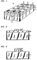
- FIG. 1 illustrates a typical optical modulator, 10, which can benefit from the present invention.
- the modulator includes a substrate, 11, comprising lithium niobate (LiNbO 3 ) which is typically approximately 1 mm thick and approx. 5 x 50 mm in size. While a lithium niobate substrate is described in this example, it will be appreciated that the invention is advantageous for any pyroelectric crystal.
- the optical waveguide path, 12, is formed in the substrate, 11, usually by diffusion of titanium through a major surface.
- a buffer layer, 13, which is a transparent dielectric layer having a refractive index less than that of the substrate.
- the layer, 13, typically comprises silicon dioxide doped with In 2 O 3 and TiO 2 .
- a charge dissipation layer, 14, is preferably deposited over the buffer layer, 13. Electrodes, 15,16, and 17, are preferably deposited over the dissipation layer. As known in the art, an electrical bias supplied to the electrodes varies the index of refraction of the waveguide path, 12, thereby modulating the intensity of any optical signal propagating through the path.
- Figs 2-7 and the flow diagram of Fig 8 illustrate a typical processing sequence for producing the device at Fig 1. It will be appreciated that several devices are fabricated from a single wafer, and only the portion of the wafer forming a single device is shown.
- the processing preferably starts with a substrate, 11, comprising LiNbO 3 having an initial bulk resistivity of typically 5 x 10 14 ohm-cm or greater at room temperature.
- a layer, 20, of metal typically comprising titanium is preferably deposited on the major surface of the substrate, 10, by standard technique such as e-beam evaporation.
- a photoresist layer, 21 is preferably deposited on the titanium layer and patterned by standard photolithographic techniques in order to expose the areas where titanium is not desired in the substrate.
- the exposed titanium is etched away. This is followed by stripping off the remaining photoresist, as illustrated in Fig 4 and step 32 of Fig 8.
- the remaining titanium is preferably diffused into the substrate, 10, to form the waveguide path, 12.
- This diffusion is typically performed in air at a temperature of approximately 1000 deg C for a time of approximately 12 hours.
- step 34 the substrate is heated in a reducing atmosphere.
- the purpose of this step is to reduce the bulk resistivity of the substrate to a value of 10 13 ohm cm or less.
- the substrate is less susceptible to temperature variants. That is, the dc bias applied to the device can remain fairly constant over a wide temperature range (-40 to 85 deg C) in spite of temperature transients within that range without significantly affecting the desired modulation of the signal propagating through the waveguide path, 12. While not being bound by any theory, it is believed that the reduction in bulk resistivity reduces the dielectric relaxation time of the substrate crystal and, therefore, does not allow substantial charge to be accumulated at the surfaces due to the pyroelectric effect which would otherwise affect the modulation.
- a resistivity of 10 13 ohm cm produces a relaxation time of approximately 30 minutes as compared to a relaxation time of 30 hours for a crystal with a resistivity of 5 x 10 14 ohm cm. Excessive reduction of resistivity should generally be avoided since the crystal becomes increasingly opaque and lossy. It is believed that a useful range of bulk resistivity is 10 11 to 10 13 ohm cm, and a preferred range is 3 x 10 12 to 10 13 ohm cm.
- the desired bulk resistivity of 10 13 ohm cm can be achieved, for example, by heating in a reducing atmosphere comprising dry nitrogen or forming gas (hydrogen and nitrogen) or vacuum at a temperature of 500 deg C for a period of approximately 1 hour. In general, temperatures in the range 350 to 800 deg C for times of 10 minutes to 10 hours may be employed. This heating step is preferably performed after the Ti diffusion step (step33) and before the formation of the buffer layer (step 35), but can also be employed at other times.
- a buffer layer, 13, is preferably formed on the top and bottom surfaces of the substrate, 11.
- This step is usually performed by sputtering at a temperature of less than 150 deg C in an atmosphere of argon and oxygen for a period of approximately 10-20 hours, followed by an annealing at a temperature of approximately 500 deg C in an atmosphere comprising moist air for a period of approximately 5 hours. It will be noted that these temperatures are not sufficient to raise the bulk resistivity of the substrate above the desired range due to the presence of the buffer layer which protects the surfaces from oxidation. In general, sputtering times in the range 6 to 20 hours, and anneal temperature in the range 450-600 deg C for a time of 3 to 24 hours may be employed.
- the charge dissipation layer, 14, is preferably formed on the buffer layer, 13, which is on the top surface of the substrate.
- the charge dissipation layer preferably usually comprises Ti/Si/N and is typically formed by sputtering at a temperature in the range 20 to 150 deg C for a period of .5 to 5 hours.
- the electrodes, 15, 16, and 17, are preferably formed on the charge dissipation layer, 14, and defined in the appropriate pattern to complete the device. Electrode formation can be done by standard techniques such as evaporation, photolithography and electroplating.
- dashed line 40 represents the boundary between two regions, 41 and 42, of the substrate 11, having different bulk resistivities.
- the boundary will desirably be formed at a depth, d, below that of the diffused region, 12, for example, a depth of approximately 30 ⁇ m.
- the bulk resistivity of the upper region, 41 is reduced to 10 13 ohm-cm or less by exposing the substrate surface to a reducing atmosphere as previously described, but for a shorter period of time, e.g., 5-15 minutes at 500 deg C. This leaves the remaining region, 42, at the original resistivity of the substrate, e.g., 5x10 14 ohm-cm.
- the upper region, 41 could have a resistivity comparable to the initial resistivity of the substrate, e.g., 5x10 14 ohm-cm, while the lower region, 42, has the reduced resisitivty of 10 13 ohm-cm or less.
- This structure can be formed by first exposing the substrate to the reducing atmosphere as previously described, and then exposing the substrate to an oxidizing atmosphere so that only the upper portion is reconverted to a resistivity of greater than 10 13 ohm-cm (e.g., 5x10 14 ohm-cm). This oxidation can be performed, for example, as a temperature in the range 500-1000 deg C for a time of 10 minutes to 24 hours.
- the invention may be employed with any pyroelectric crystal such as LiTaO 3 , BaNaNb 2 O 5 , and KTaNbO 3 having a similar relationship of electrical conductivity to oxidation/reduction of the oxide crystal.
- a pyroelectric crystal such as LiTaO 3 , BaNaNb 2 O 5 , and KTaNbO 3 having a similar relationship of electrical conductivity to oxidation/reduction of the oxide crystal.
- an optical modulator has been described, the invention may be employed in any optical waveguide device employing a pyroelectric crystal, such as attenuators, optical switches, and polarization controls and scramblers.
Landscapes
- Physics & Mathematics (AREA)
- Nonlinear Science (AREA)
- General Physics & Mathematics (AREA)
- Optics & Photonics (AREA)
- Chemical & Material Sciences (AREA)
- Engineering & Computer Science (AREA)
- Ceramic Engineering (AREA)
- Crystallography & Structural Chemistry (AREA)
- Optical Integrated Circuits (AREA)
- Optical Modulation, Optical Deflection, Nonlinear Optics, Optical Demodulation, Optical Logic Elements (AREA)
Abstract
Description
- This invention relates to optical waveguide devices such as lithium niobate devices
- Optical waveguide devices typically employ lithium niobate (LiNbO3) or lithium tantalate (LiTaO3) substrates with a defined waveguide path, and bias electrodes formed over the substrate. They may also include a buffer oxide between the electrodes and substrate. An electrical bias supplied to the electrodes alters the index of refraction of the waveguide path so that the device may be employed as a high speed optical switch, modulator, attentuator or other type of optical device.
- For proper operation of such devices, it is highly desirable that a do electric field bias be maintained In the waveguide for extended times and varying temperatures. Therefore, long term bias stability is a critical concern. Most approaches to providing bias stability have involved reducing OH or proton concentration on the lithium niobate substrate (Nagata et al "Improved Long Term Drift In OH-Reduced Lithium Niobate Optical Intensity Modulators", Optics & Photonics News, vol. 7, Engineering & Laboratory Notes (1996) and Koide, et al "Prevention of Thermal Degradation by Using Dehydrated LiNbO3 Crystal" Jpn. J. App Phy., vol. 33, pp. L957-L958 (1994)), removal of a damaged layer from the surface of the lithium niobate substrate (Minikata et al, "DC Drift Free Ti Diffused LiNbO3 Optical Modulators" Bulletin of the Research Institute of Electronics, vol. 30, pp. 209-212 (1995)), or modification of the composition of the buffer layer (EP 0 553 568 A1). Such approaches appear effective in eliminating long term drift. However, pyroelectric material, such as lithium niobate and lithium tantalate, is also sensitive to temperature variations. That is, temperature variations induce charge build-up at the surfaces of the substrate, and this build-up generally requires an increasing bias to achieve the desired modulation. The above solutions do not deal with bias instability due to such temperature variations.
- One approach to the instability problem is to provide a semi-insulation charge dissipation layer, such as partially oxidized polysilicon or Ti/Si/N, over the substrate. We have found, however, that the effectiveness of this charge dissipation layer can degrade under bias over a period of time, thus limiting its effectiveness.
- It has also been suggested that lithium niobate material used for surface acoustic wave devices can be treated by heating in a forming gas (10 percent H2, 90 percent N2) for one hour at temperatures in the range 400-750 deg C. (see Standifer et al "Chemically Reduced Lithium Niobate Single Crystals..." IEEE Frequency Control Symposium, May 27- 29, 1998, pp. 470 to 472.) This is done to suppress sparking during processing and operation as well as reduce optical reflections during photolithographic processing of the device.
- The invention in accordance with one aspect is an optical waveguide device including a substrate comprising a pyroelectric crystal, where the bulk resistivity of at least a portion of the substrate is no greater than 1013 ohm cm. In accordance with another aspect, the invention is a method of forming an optical waveguide device including the steps of providing a substrate comprising a pyroelectric crystal having a certain bulk resistivity, and heating the substrate in a reducing atmosphere for a time and temperature sufficient to reduce the bulk resistivity to no greater than 1013 ohm cm.
- These and other features of the invention are delineated in detail in the following description. In the drawing:
- Fig 1 is a perspective view of a typical waveguide device which incorporates the present invention in accordance with one embodiment;
- Figs 2- 7 are end views of the device during various stages of fabrication in accordance with the same embodiment;
- Fig 8 is a flow diagram illustrating the method aspects of the invention in accordance with one embodiment; and
- Fig. 9 is an end view of the device in accordance with alternative embodiments of the invention.
-
- It will be appreciated that, for purposes of illustration, these figures are not necessarily drawn to scale.
- Figure 1 illustrates a typical optical modulator, 10, which can benefit from the present invention. The modulator includes a substrate, 11, comprising lithium niobate (LiNbO3) which is typically approximately 1 mm thick and approx. 5 x 50 mm in size. While a lithium niobate substrate is described in this example, it will be appreciated that the invention is advantageous for any pyroelectric crystal. The optical waveguide path, 12, is formed in the substrate, 11, usually by diffusion of titanium through a major surface. Preferably deposited on the major surface of the substrate is a buffer layer, 13, which is a transparent dielectric layer having a refractive index less than that of the substrate. The layer, 13, typically comprises silicon dioxide doped with In2O3 and TiO2. A charge dissipation layer, 14, is preferably deposited over the buffer layer, 13. Electrodes, 15,16, and 17, are preferably deposited over the dissipation layer. As known in the art, an electrical bias supplied to the electrodes varies the index of refraction of the waveguide path, 12, thereby modulating the intensity of any optical signal propagating through the path.
- Figs 2-7 and the flow diagram of Fig 8 illustrate a typical processing sequence for producing the device at Fig 1. It will be appreciated that several devices are fabricated from a single wafer, and only the portion of the wafer forming a single device is shown.
- The processing preferably starts with a substrate, 11, comprising LiNbO3 having an initial bulk resistivity of typically 5 x 10¹⁴ ohm-cm or greater at room temperature. As illustrated in Fig 2 and by
step 30 in Fig 8, a layer, 20, of metal typically comprising titanium is preferably deposited on the major surface of the substrate, 10, by standard technique such as e-beam evaporation. A photoresist layer, 21 is preferably deposited on the titanium layer and patterned by standard photolithographic techniques in order to expose the areas where titanium is not desired in the substrate. As illustrated in Fig 3 andstep 31 of Fig 8, the exposed titanium is etched away. This is followed by stripping off the remaining photoresist, as illustrated in Fig 4 andstep 32 of Fig 8. - Next, as illustrated in Fig 5, and
step 33, the remaining titanium is preferably diffused into the substrate, 10, to form the waveguide path, 12. This diffusion is typically performed in air at a temperature of approximately 1000 deg C for a time of approximately 12 hours. - Next, as illustrated by
step 34, the substrate is heated in a reducing atmosphere. The purpose of this step is to reduce the bulk resistivity of the substrate to a value of 1013 ohm cm or less. Applicants have discovered that by reducing the resistivity, the substrate is less susceptible to temperature variants. That is, the dc bias applied to the device can remain fairly constant over a wide temperature range (-40 to 85 deg C) in spite of temperature transients within that range without significantly affecting the desired modulation of the signal propagating through the waveguide path, 12. While not being bound by any theory, it is believed that the reduction in bulk resistivity reduces the dielectric relaxation time of the substrate crystal and, therefore, does not allow substantial charge to be accumulated at the surfaces due to the pyroelectric effect which would otherwise affect the modulation. In particular, a resistivity of 1013 ohm cm produces a relaxation time of approximately 30 minutes as compared to a relaxation time of 30 hours for a crystal with a resistivity of 5 x 10¹⁴ ohm cm. Excessive reduction of resistivity should generally be avoided since the crystal becomes increasingly opaque and lossy. It is believed that a useful range of bulk resistivity is 1011 to 1013 ohm cm, and a preferred range is 3 x 10¹² to 1013 ohm cm. - The desired bulk resistivity of 1013 ohm cm can be achieved, for example, by heating in a reducing atmosphere comprising dry nitrogen or forming gas (hydrogen and nitrogen) or vacuum at a temperature of 500 deg C for a period of approximately 1 hour. In general, temperatures in the range 350 to 800 deg C for times of 10 minutes to 10 hours may be employed. This heating step is preferably performed after the Ti diffusion step (step33) and before the formation of the buffer layer (step 35), but can also be employed at other times.
- As iliustrated in Fig 6 and
step 35, a buffer layer, 13, is preferably formed on the top and bottom surfaces of the substrate, 11. This step is usually performed by sputtering at a temperature of less than 150 deg C in an atmosphere of argon and oxygen for a period of approximately 10-20 hours, followed by an annealing at a temperature of approximately 500 deg C in an atmosphere comprising moist air for a period of approximately 5 hours. It will be noted that these temperatures are not sufficient to raise the bulk resistivity of the substrate above the desired range due to the presence of the buffer layer which protects the surfaces from oxidation. In general, sputtering times in the range 6 to 20 hours, and anneal temperature in the range 450-600 deg C for a time of 3 to 24 hours may be employed. - Next (step 36), the charge dissipation layer, 14, is preferably formed on the buffer layer, 13, which is on the top surface of the substrate. The charge dissipation layer preferably usually comprises Ti/Si/N and is typically formed by sputtering at a temperature in the
range 20 to 150 deg C for a period of .5 to 5 hours. - As illustrated in Fig 7, and step 37 of Fig 8, the electrodes, 15, 16, and 17, are preferably formed on the charge dissipation layer, 14, and defined in the appropriate pattern to complete the device. Electrode formation can be done by standard techniques such as evaporation, photolithography and electroplating.
- While the above-described embodiment has involved reducing the bulk resistivity of the substrate through its entire depth, it will be appreciated that reducing resistivity for only a portion of its depth may also be advantageous. Such embodiments are illustrated in the end view of Fig. 9, where elements similar to the previous figures are similarly numbered. Specifically, dashed line 40 represents the boundary between two regions, 41 and 42, of the
substrate 11, having different bulk resistivities. The boundary will desirably be formed at a depth, d, below that of the diffused region, 12, for example, a depth of approximately 30 µm. In one embodiment, the bulk resistivity of the upper region, 41, is reduced to 1013 ohm-cm or less by exposing the substrate surface to a reducing atmosphere as previously described, but for a shorter period of time, e.g., 5-15 minutes at 500 deg C. This leaves the remaining region, 42, at the original resistivity of the substrate, e.g., 5x10¹⁴ ohm-cm. - In an alternative embodiment, the upper region, 41, could have a resistivity comparable to the initial resistivity of the substrate, e.g., 5x10¹⁴ ohm-cm, while the lower region, 42, has the reduced resisitivty of 1013 ohm-cm or less. This structure can be formed by first exposing the substrate to the reducing atmosphere as previously described, and then exposing the substrate to an oxidizing atmosphere so that only the upper portion is reconverted to a resistivity of greater than 1013 ohm-cm (e.g., 5x10¹⁴ ohm-cm). This oxidation can be performed, for example, as a temperature in the range 500-1000 deg C for a time of 10 minutes to 24 hours.
- Is will also he appreciated that there may not be a sharp boundary, 40, between the regions of different restrictions. Rather, the resistivity may be graded.
- Various additional modifications of the invention will become apparent to those skilled in the art. For example, although a lithium niobate substrate is described, the invention may be employed with any pyroelectric crystal such as LiTaO3, BaNaNb2O5, and KTaNbO3 having a similar relationship of electrical conductivity to oxidation/reduction of the oxide crystal. Further, although an optical modulator has been described, the invention may be employed in any optical waveguide device employing a pyroelectric crystal, such as attenuators, optical switches, and polarization controls and scramblers.
Claims (22)
- An optical waveguide device (10) including a substrate (11) comprising a pyroelectric crystal, where the bulk resistivity of at least a portion of the substrate is no greater than 1013 ohm cm.
- The device according to claim 1 wherein the substrate is selected from the group consisting of LiNbO3 and LiTaO3.
- The device according to claim 1 wherein the bulk resistivity is within the range 1011 to 1013 ohm cm.
- The device according to claim 1 wherein the bulk resistivity is within the range 3 x 10¹² to 1013 ohm cm.
- The device according to claim 1 wherein the device is an optical modulator.
- The device according to claim 1 further comprising a buffer layer (13) on at least one major surface of the substrate.
- The device according to claim 6 further comprising a charge dissipation layer (14) on the buffer layer.
- The device according to claim 1 wherein the waveguide comprises a region (12) of diffused material.
- The device according to claim 8 wherein the diffused material comprises titanium.
- The device according to claim 1 further comprising electrodes (15, 16, 17) formed over the substrate so as to affect the index of refraction of the waveguide when an electrical bias is supplied thereto
- The device according to claim 1 wherein the substrate has a depth, and the bulk resistivity is no greater than 1013 ohm cm for the entire depth.
- The device according to claim 1, wherein the substrate has a depth, and only a portion (d) of the depth has a bulk resistivity of no greater than 1013 ohm cm.
- A method of forming an optical waveguide device (10) including the steps of providing a substrate (11) comprising a pyroelectric crystal having a certain bulk resistivity, and heating the substrate in a reducing atmosphere for a time and temperature sufficient to reduce at least a portion of the bulk resistivity to no greater than 1013 ohm cm.
- The method according to claim 13 wherein the resistivity is reduced to a range of 1011 to 1013 ohm cm
- The method according to claim 13 wherein the resistivity is reduced to a range of 3 x 10¹² to 1013 ohm cm.
- The method according to claim 13 wherein the substrate is heated at a temperature in the range 350 to 800 deg C for a period within the range 10 minutes to 10 hours.
- The method according to claim 13 further comprising the steps of diffusing a material into the substrate to form the waveguide (12), and forming a buffer layer (13) on at least one major surface of the substrate.
- The method according to claim 17 wherein the heating to reduce bulk resistivity is done after the diffusion and before the formation of the buffer layer.
- The method according to claim 18 wherein the buffer layer is formed by sputtering at a temperature of less than 150 deg C in an atmosphere of argon and oxygen for a period of approximately 6-20 hours, followed by an annealing at a temperature in the range of 450-600 deg C in an atmosphere comprising air for a period of 3-24 hours.
- The method according to claim 13 wherein the substrate has a depth and is heated for a time and temperature sufficient to reduce the bulk resistivity of the entire depth of the substrate.
- The method according to claim 13 wherein the substrate has a depth, and the substrate is heated for a time and temperature sufficient to reduce only a portion of the depth to a resistivity of no greater than 1013 ohm cm.
- The method according to claim 13 further comprising heating the substrate in an oxidizing, atmosphere so that only a portion of the substrate removed from the surface has a bulk resistivity of no greater than 1013 ohm cm.
Applications Claiming Priority (2)
| Application Number | Priority Date | Filing Date | Title |
|---|---|---|---|
| US287683 | 1999-04-07 | ||
| US09/287,683 US6282356B1 (en) | 1999-04-07 | 1999-04-07 | Optical waveguide device with enhanced stability |
Publications (2)
| Publication Number | Publication Date |
|---|---|
| EP1043617A1 true EP1043617A1 (en) | 2000-10-11 |
| EP1043617B1 EP1043617B1 (en) | 2003-01-08 |
Family
ID=23103910
Family Applications (1)
| Application Number | Title | Priority Date | Filing Date |
|---|---|---|---|
| EP00302815A Expired - Lifetime EP1043617B1 (en) | 1999-04-07 | 2000-04-04 | Optical waveguide device with enhanced stability |
Country Status (5)
| Country | Link |
|---|---|
| US (1) | US6282356B1 (en) |
| EP (1) | EP1043617B1 (en) |
| JP (1) | JP2000352700A (en) |
| CA (1) | CA2303674A1 (en) |
| DE (1) | DE60001124T2 (en) |
Cited By (4)
| Publication number | Priority date | Publication date | Assignee | Title |
|---|---|---|---|---|
| WO2002023261A1 (en) * | 2000-09-18 | 2002-03-21 | Sumitomo Osaka Cement Co., Ltd. | Optical waveguide type optical modulator and production method therefor |
| EP1518947A3 (en) * | 2003-09-26 | 2007-03-07 | Shin-Etsu Chemical Co., Ltd. | Method of producing single-polarized lithium tantalate crystal and crystal thereby obtained. |
| US7323050B2 (en) | 2003-03-06 | 2008-01-29 | Shin-Etsu Chemical Co., Ltd. | Method of producing lithium tantalate crystal |
| WO2010105715A1 (en) * | 2009-03-16 | 2010-09-23 | Perkinelmer Optoelectronics Gmbh & Co.Kg | Pyroelectric material - radiation sensor - method of making a radiation sensor - use of lithium tantalate and lithium niobate |
Families Citing this family (8)
| Publication number | Priority date | Publication date | Assignee | Title |
|---|---|---|---|---|
| FR2820217B1 (en) * | 2001-01-31 | 2003-04-18 | Teem Photonics | INTEGRATED OPTICAL STRUCTURE HAVING AT LEAST ONE UNDERGROUND GUIDE PORTION AND ITS MANUFACTURING METHOD |
| JP2005119907A (en) * | 2003-10-16 | 2005-05-12 | Sumitomo Metal Mining Co Ltd | Lithium tantalate substrate and its producing method |
| DE602005008922D1 (en) * | 2004-04-02 | 2008-09-25 | Northrop Grumman Corp | IMPLEMENTATION OF ONE OR MORE OPTICAL WAVEGUIDE IN REDUCED OPTICAL MATERIAL |
| US7324257B2 (en) * | 2004-07-27 | 2008-01-29 | Jds Uniphase Corporation | Low bias drift modulator with buffer layer |
| US7405861B2 (en) | 2004-09-27 | 2008-07-29 | Idc, Llc | Method and device for protecting interferometric modulators from electrostatic discharge |
| JP4708905B2 (en) * | 2005-08-05 | 2011-06-22 | イビデン株式会社 | Thin film embedded capacitance, manufacturing method thereof, and printed wiring board |
| US7228046B1 (en) * | 2005-11-23 | 2007-06-05 | Honeywell International, Inc. | Environmentally stable electro-optic device and method for making same |
| US7844149B2 (en) * | 2007-01-12 | 2010-11-30 | Jds Uniphase Corporation | Humidity tolerant electro-optic device |
Citations (6)
| Publication number | Priority date | Publication date | Assignee | Title |
|---|---|---|---|---|
| JPH0566428A (en) * | 1991-09-05 | 1993-03-19 | Nec Corp | Light control device |
| JPH05158001A (en) * | 1991-12-06 | 1993-06-25 | Nippon Telegr & Teleph Corp <Ntt> | Optical control device |
| US5388170A (en) * | 1993-11-22 | 1995-02-07 | At&T Corp. | Electrooptic device structure and method for reducing thermal effects in optical waveguide modulators |
| US5679291A (en) * | 1995-01-13 | 1997-10-21 | Fujitsu Limited | Method of fabricating optical waveguide device |
| US5680497A (en) * | 1991-12-27 | 1997-10-21 | Fujitsu Limited | Optical waveguide device |
| EP0893515A1 (en) * | 1997-07-25 | 1999-01-27 | Crystal Technology, Inc. | Preconditioned crystals of lithium niobate and lithium tantalate and methods of preparing the same |
-
1999
- 1999-04-07 US US09/287,683 patent/US6282356B1/en not_active Expired - Lifetime
-
2000
- 2000-04-03 CA CA002303674A patent/CA2303674A1/en not_active Abandoned
- 2000-04-04 DE DE60001124T patent/DE60001124T2/en not_active Expired - Lifetime
- 2000-04-04 EP EP00302815A patent/EP1043617B1/en not_active Expired - Lifetime
- 2000-04-06 JP JP2000104831A patent/JP2000352700A/en active Pending
Patent Citations (6)
| Publication number | Priority date | Publication date | Assignee | Title |
|---|---|---|---|---|
| JPH0566428A (en) * | 1991-09-05 | 1993-03-19 | Nec Corp | Light control device |
| JPH05158001A (en) * | 1991-12-06 | 1993-06-25 | Nippon Telegr & Teleph Corp <Ntt> | Optical control device |
| US5680497A (en) * | 1991-12-27 | 1997-10-21 | Fujitsu Limited | Optical waveguide device |
| US5388170A (en) * | 1993-11-22 | 1995-02-07 | At&T Corp. | Electrooptic device structure and method for reducing thermal effects in optical waveguide modulators |
| US5679291A (en) * | 1995-01-13 | 1997-10-21 | Fujitsu Limited | Method of fabricating optical waveguide device |
| EP0893515A1 (en) * | 1997-07-25 | 1999-01-27 | Crystal Technology, Inc. | Preconditioned crystals of lithium niobate and lithium tantalate and methods of preparing the same |
Non-Patent Citations (3)
| Title |
|---|
| E.M.STANDIFER ET AL: "Chemically reduced lithium niobate single crystals:processing,properties and improvements in saw device fabrication and performance", PROCEEDINGS OF THE 1998 IEEE INTERNATIONAL FREQUENCY CONTROL SYMPOSIUM, 27 May 1998 (1998-05-27) - 29 May 1998 (1998-05-29), Pasadena ,CA,USA, pages 470 - 472, XP002143619 * |
| PATENT ABSTRACTS OF JAPAN vol. 017, no. 387 (P - 1576) 20 July 1993 (1993-07-20) * |
| PATENT ABSTRACTS OF JAPAN vol. 017, no. 553 (P - 1625) 5 October 1993 (1993-10-05) * |
Cited By (7)
| Publication number | Priority date | Publication date | Assignee | Title |
|---|---|---|---|---|
| WO2002023261A1 (en) * | 2000-09-18 | 2002-03-21 | Sumitomo Osaka Cement Co., Ltd. | Optical waveguide type optical modulator and production method therefor |
| US6956980B2 (en) | 2000-09-18 | 2005-10-18 | Sumitomo Osaka Cement Co., Ltd. | Optical waveguide type optical modulator and production method therefor |
| US7323050B2 (en) | 2003-03-06 | 2008-01-29 | Shin-Etsu Chemical Co., Ltd. | Method of producing lithium tantalate crystal |
| EP1600531A4 (en) * | 2003-03-06 | 2009-04-01 | Shinetsu Chemical Co | PROCESS FOR PRODUCING LITHIUM TANTALATE CRYSTAL |
| EP1518947A3 (en) * | 2003-09-26 | 2007-03-07 | Shin-Etsu Chemical Co., Ltd. | Method of producing single-polarized lithium tantalate crystal and crystal thereby obtained. |
| US7374612B2 (en) | 2003-09-26 | 2008-05-20 | Shin-Etsu Chemical Co., Ltd. | Method of producing single-polarized lithium tantalate crystal and single-polarized lithium tantalate crystal |
| WO2010105715A1 (en) * | 2009-03-16 | 2010-09-23 | Perkinelmer Optoelectronics Gmbh & Co.Kg | Pyroelectric material - radiation sensor - method of making a radiation sensor - use of lithium tantalate and lithium niobate |
Also Published As
| Publication number | Publication date |
|---|---|
| JP2000352700A (en) | 2000-12-19 |
| CA2303674A1 (en) | 2000-10-07 |
| DE60001124D1 (en) | 2003-02-13 |
| DE60001124T2 (en) | 2003-09-11 |
| US6282356B1 (en) | 2001-08-28 |
| EP1043617B1 (en) | 2003-01-08 |
Similar Documents
| Publication | Publication Date | Title |
|---|---|---|
| US6282356B1 (en) | Optical waveguide device with enhanced stability | |
| US6374005B2 (en) | Integrated optic device produced by cyclically annealed proton exchange process | |
| EP1022605B1 (en) | Optical waveguide device | |
| EP0554593B1 (en) | A method of manufacturing a device employing a substrate of a material that exhibits the pyroelectric effect | |
| JPH07199134A (en) | Optoelectronic device structure and method for reducing temperature effects in optical waveguide modulators | |
| US4751196A (en) | High voltage thin film transistor on PLZT and method of manufacture thereof | |
| JPH083581B2 (en) | Electro-optical mode converter | |
| CA2422619A1 (en) | Optical waveguide type optical modulator and production method therefor | |
| US6195191B1 (en) | Optical devices having improved temperature stability | |
| JP3710686B2 (en) | Electro-optic element | |
| US4714312A (en) | Electrostatically biased electrooptical devices | |
| US6480633B1 (en) | Electro-optic device including a buffer layer of transparent conductive material | |
| WO2025101981A1 (en) | Thin film lithium-containing photonics wafer having a trap-rich substrate | |
| CA2377949C (en) | Electro-optic element | |
| EP0982619A2 (en) | A light control device and a method for manufacturing the same | |
| JP3021888B2 (en) | Optical waveguide functional element and method of manufacturing the same | |
| JP2003066393A (en) | Integrated optical waveguide device | |
| JPWO2001001190A1 (en) | Electro-optical element and its manufacturing method | |
| JPH0675195A (en) | Optical control device | |
| JP4137680B2 (en) | Manufacturing method of light control element | |
| JPH05215927A (en) | Optical integrated circuit and its production | |
| JPH09269469A (en) | Optical waveguide device | |
| JP3050202B2 (en) | Optical waveguide device and method of manufacturing the same | |
| JPH10104559A (en) | Optical waveguide device | |
| JPH05113513A (en) | Waveguide optical device and manufacturing method thereof |
Legal Events
| Date | Code | Title | Description |
|---|---|---|---|
| PUAI | Public reference made under article 153(3) epc to a published international application that has entered the european phase |
Free format text: ORIGINAL CODE: 0009012 |
|
| 17P | Request for examination filed |
Effective date: 20000413 |
|
| AK | Designated contracting states |
Kind code of ref document: A1 Designated state(s): DE FR GB |
|
| AX | Request for extension of the european patent |
Free format text: AL;LT;LV;MK;RO;SI |
|
| 17Q | First examination report despatched |
Effective date: 20001016 |
|
| AKX | Designation fees paid | ||
| RBV | Designated contracting states (corrected) |
Designated state(s): DE FR GB |
|
| RAP1 | Party data changed (applicant data changed or rights of an application transferred) |
Owner name: AGERE SYSTEMS OPTOELECTRONICS GUARDIAN CORPORATION |
|
| GRAG | Despatch of communication of intention to grant |
Free format text: ORIGINAL CODE: EPIDOS AGRA |
|
| GRAG | Despatch of communication of intention to grant |
Free format text: ORIGINAL CODE: EPIDOS AGRA |
|
| GRAH | Despatch of communication of intention to grant a patent |
Free format text: ORIGINAL CODE: EPIDOS IGRA |
|
| GRAH | Despatch of communication of intention to grant a patent |
Free format text: ORIGINAL CODE: EPIDOS IGRA |
|
| GRAA | (expected) grant |
Free format text: ORIGINAL CODE: 0009210 |
|
| AK | Designated contracting states |
Kind code of ref document: B1 Designated state(s): DE FR GB |
|
| REG | Reference to a national code |
Ref country code: GB Ref legal event code: FG4D |
|
| REF | Corresponds to: |
Ref document number: 60001124 Country of ref document: DE Date of ref document: 20030213 Kind code of ref document: P |
|
| ET | Fr: translation filed | ||
| PLBE | No opposition filed within time limit |
Free format text: ORIGINAL CODE: 0009261 |
|
| STAA | Information on the status of an ep patent application or granted ep patent |
Free format text: STATUS: NO OPPOSITION FILED WITHIN TIME LIMIT |
|
| 26N | No opposition filed |
Effective date: 20031009 |
|
| PGFP | Annual fee paid to national office [announced via postgrant information from national office to epo] |
Ref country code: DE Payment date: 20120419 Year of fee payment: 13 |
|
| PGFP | Annual fee paid to national office [announced via postgrant information from national office to epo] |
Ref country code: FR Payment date: 20120504 Year of fee payment: 13 Ref country code: GB Payment date: 20120404 Year of fee payment: 13 |
|
| GBPC | Gb: european patent ceased through non-payment of renewal fee |
Effective date: 20130404 |
|
| PG25 | Lapsed in a contracting state [announced via postgrant information from national office to epo] |
Ref country code: GB Free format text: LAPSE BECAUSE OF NON-PAYMENT OF DUE FEES Effective date: 20130404 Ref country code: DE Free format text: LAPSE BECAUSE OF NON-PAYMENT OF DUE FEES Effective date: 20131101 |
|
| REG | Reference to a national code |
Ref country code: FR Ref legal event code: ST Effective date: 20131231 |
|
| REG | Reference to a national code |
Ref country code: DE Ref legal event code: R119 Ref document number: 60001124 Country of ref document: DE Effective date: 20131101 |
|
| PG25 | Lapsed in a contracting state [announced via postgrant information from national office to epo] |
Ref country code: FR Free format text: LAPSE BECAUSE OF NON-PAYMENT OF DUE FEES Effective date: 20130430 |