EP1043135A2 - Teflon mould-releasing film used by encapsulating semiconductor chip - Google Patents
Teflon mould-releasing film used by encapsulating semiconductor chip Download PDFInfo
- Publication number
- EP1043135A2 EP1043135A2 EP00104106A EP00104106A EP1043135A2 EP 1043135 A2 EP1043135 A2 EP 1043135A2 EP 00104106 A EP00104106 A EP 00104106A EP 00104106 A EP00104106 A EP 00104106A EP 1043135 A2 EP1043135 A2 EP 1043135A2
- Authority
- EP
- European Patent Office
- Prior art keywords
- mold
- film
- resin
- polytetrafluoroethylene
- encapsulating
- Prior art date
- Legal status (The legal status is an assumption and is not a legal conclusion. Google has not performed a legal analysis and makes no representation as to the accuracy of the status listed.)
- Withdrawn
Links
Images

Classifications
-
- H—ELECTRICITY
- H10—SEMICONDUCTOR DEVICES; ELECTRIC SOLID-STATE DEVICES NOT OTHERWISE PROVIDED FOR
- H10W—GENERIC PACKAGES, INTERCONNECTIONS, CONNECTORS OR OTHER CONSTRUCTIONAL DETAILS OF DEVICES COVERED BY CLASS H10
- H10W74/00—Encapsulations, e.g. protective coatings
- H10W74/01—Manufacture or treatment
- H10W74/016—Manufacture or treatment using moulds
-
- B—PERFORMING OPERATIONS; TRANSPORTING
- B29—WORKING OF PLASTICS; WORKING OF SUBSTANCES IN A PLASTIC STATE IN GENERAL
- B29C—SHAPING OR JOINING OF PLASTICS; SHAPING OF MATERIAL IN A PLASTIC STATE, NOT OTHERWISE PROVIDED FOR; AFTER-TREATMENT OF THE SHAPED PRODUCTS, e.g. REPAIRING
- B29C45/00—Injection moulding, i.e. forcing the required volume of moulding material through a nozzle into a closed mould; Apparatus therefor
- B29C45/14—Injection moulding, i.e. forcing the required volume of moulding material through a nozzle into a closed mould; Apparatus therefor incorporating preformed parts or layers, e.g. injection moulding around inserts or for coating articles
- B29C45/14639—Injection moulding, i.e. forcing the required volume of moulding material through a nozzle into a closed mould; Apparatus therefor incorporating preformed parts or layers, e.g. injection moulding around inserts or for coating articles for obtaining an insulating effect, e.g. for electrical components
- B29C45/14655—Injection moulding, i.e. forcing the required volume of moulding material through a nozzle into a closed mould; Apparatus therefor incorporating preformed parts or layers, e.g. injection moulding around inserts or for coating articles for obtaining an insulating effect, e.g. for electrical components connected to or mounted on a carrier, e.g. lead frame
-
- B—PERFORMING OPERATIONS; TRANSPORTING
- B29—WORKING OF PLASTICS; WORKING OF SUBSTANCES IN A PLASTIC STATE IN GENERAL
- B29C—SHAPING OR JOINING OF PLASTICS; SHAPING OF MATERIAL IN A PLASTIC STATE, NOT OTHERWISE PROVIDED FOR; AFTER-TREATMENT OF THE SHAPED PRODUCTS, e.g. REPAIRING
- B29C45/00—Injection moulding, i.e. forcing the required volume of moulding material through a nozzle into a closed mould; Apparatus therefor
- B29C45/14—Injection moulding, i.e. forcing the required volume of moulding material through a nozzle into a closed mould; Apparatus therefor incorporating preformed parts or layers, e.g. injection moulding around inserts or for coating articles
- B29C45/14639—Injection moulding, i.e. forcing the required volume of moulding material through a nozzle into a closed mould; Apparatus therefor incorporating preformed parts or layers, e.g. injection moulding around inserts or for coating articles for obtaining an insulating effect, e.g. for electrical components
- B29C45/14655—Injection moulding, i.e. forcing the required volume of moulding material through a nozzle into a closed mould; Apparatus therefor incorporating preformed parts or layers, e.g. injection moulding around inserts or for coating articles for obtaining an insulating effect, e.g. for electrical components connected to or mounted on a carrier, e.g. lead frame
- B29C2045/14663—Injection moulding, i.e. forcing the required volume of moulding material through a nozzle into a closed mould; Apparatus therefor incorporating preformed parts or layers, e.g. injection moulding around inserts or for coating articles for obtaining an insulating effect, e.g. for electrical components connected to or mounted on a carrier, e.g. lead frame the mould cavity walls being lined with a film, e.g. release film
-
- B—PERFORMING OPERATIONS; TRANSPORTING
- B29—WORKING OF PLASTICS; WORKING OF SUBSTANCES IN A PLASTIC STATE IN GENERAL
- B29K—INDEXING SCHEME ASSOCIATED WITH SUBCLASSES B29B, B29C OR B29D, RELATING TO MOULDING MATERIALS OR TO MATERIALS FOR MOULDS, REINFORCEMENTS, FILLERS OR PREFORMED PARTS, e.g. INSERTS
- B29K2027/00—Use of polyvinylhalogenides or derivatives thereof as moulding material
- B29K2027/12—Use of polyvinylhalogenides or derivatives thereof as moulding material containing fluorine
- B29K2027/18—PTFE, i.e. polytetrafluoroethylene, e.g. ePTFE, i.e. expanded polytetrafluoroethylene
-
- H—ELECTRICITY
- H10—SEMICONDUCTOR DEVICES; ELECTRIC SOLID-STATE DEVICES NOT OTHERWISE PROVIDED FOR
- H10W—GENERIC PACKAGES, INTERCONNECTIONS, CONNECTORS OR OTHER CONSTRUCTIONAL DETAILS OF DEVICES COVERED BY CLASS H10
- H10W90/00—Package configurations
- H10W90/701—Package configurations characterised by the relative positions of pads or connectors relative to package parts
- H10W90/751—Package configurations characterised by the relative positions of pads or connectors relative to package parts of bond wires
- H10W90/756—Package configurations characterised by the relative positions of pads or connectors relative to package parts of bond wires between a chip and a stacked lead frame, conducting package substrate or heat sink
Definitions
- the present invention relates to a method of resin-encapsulating a semiconductor chip and a mold-releasing film used in the method.
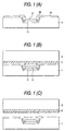
- Fig. 1 shows QFN (Quad Flat Package) of the structure formed by removing the lower surface mold portion from QFP and cutting off the lead at the side from the mold side portion.
- the electrode of a semiconductor chip 2 is bonded to the terminal 22 of each lead frame 21 with a wire, the semiconductor chip 2 is placed in the cavity 11 of a lower mold 1 with the terminals 22 being at the upper side as shown in Fig. 1.
- the mold is closed by an upper mold 3 via a polytetrafluoroethylene film F and a resin is injected into the cavity by a transfer molding and is simultaneously cured as shown in Fig. 1 (B), the mold is then opened as shown in Fig. 1 (C), and the lead frames are trimmed leaving the terminals.
- the terminals bites into the polytetrafluoroethylene film by the mold closing pressure, whereby the terminals and the polytetrafluoroethylene film are always maintained at a contact state during resin encapsulating to exclude the occurrence of resin covering of the terminals.
- the polytetrafluoroethylene film can be obtained by a casting method (a method of coating a dispersion of polytetrafluoroethylene on a carrier sheet followed by sintering and releasing the sintered film from the carrier sheet), a cutting method (a method of sintering a polytetrafluoroethylene rod and cutting the rod by a cutting lathe into a film), etc.
- the inventors made the investigations on the cause thereof and have found that the cause is in the difference in the thermal shrinkage percentages between the lengthwise direction and the width direction of the mold-releasing film. That is, it is presumed that when a film has a directional property in the thermal shrinkage percentage, a force which shears and deforms the film slantingly is applied to the film to thereby cause creases.
- an object of the present invention is to provide a method of carrying out resin encapsulating of a semiconductor chip using the polytetrafluoroethylene film as the mold-releasing film, wherein resin encapsulating can be carried out at an excellent yield while preventing the occurrence of resin covering of the terminals or the top surfaces of electrodes.
- the first aspect of this invention is a method of resin-encapsulating a semiconductor chip by closing a lower mold having disposed in a cavity thereof a semiconductor chip equipped with terminals or post electrodes by an upper mold via a mold-releasing film made of a polytetrafluoroethylene film between the surface on which the terminals or the post electrodes are disposed and the upper mold and then injecting a resin into the cavity of the lower mold while curing, wherein a polytetrafluoroethylene film satisfies the conditions that the thermal shrinkage percentages in the longitudinal and width directions are 5% or lower, the difference between the thermal shrinkage percentages is within 3%; and the ratio of the elastic modulus of the longitudinal direction to the elastic modulus of the width direction is from 0.5 to 2.0 during resin encapsulating.
- the second aspect of this invention is a mold-releasing film used for a method of resin-encapsulating a semiconductor chip, wherein the mold-releasing film is made of a polytetrafluoroethylene film satisfying the conditions that the thermal shrinkage percentages in the longitudinal and width directions at 175°C for 10 minutes are 5% or lower, the difference between the thermal shrinkage percentages is within 3%, and the ratio of the elastic modulus of the longitudinal direction to the elastic modulus of the width direction is from 0.5 to 2.0, and preferably from 0.8 to 1.5 during resin encapsulating.
- the breaking elongation percentages in the longitudinal direction and the width direction thereof at 175°C are both at least 600% and further it is preferred that the surface roughness Ra (by a JIS B 0601 method) thereof is 0.3 ⁇ m or lower, and preferably 0.2 ⁇ m or lower.
- the polytetrafluoroethylene film used for resin encapsulating a semiconductor chip in this invention that is, the polytetrafluoroethylene film satisfying the conditions that the thermal shrinkage percentages in the longitudinal and width directions at 175°C for 10 minutes are 5% or lower, the difference between the thermal shrinkage percentages is within 3%, and the ratio of the elastic modulus of the longitudinal direction to the elastic modulus of the width direction is from 0.5 to 2.0, and preferably from 0.8 to 1.5, can be obtained by a casting method.
- the polytetrafluoroethylene film can be obtained by coating a dispersion of polytetrafluoroethylene on a heat-resisting carrier sheet, sintering it at a temperature of at least the melting point of polytetrafluoroethylene, and then releasing the sintered film from the carrier sheet.
- the coated layer may be sintered by one-stage heating at a single stroke but it is preferred to use multistage heating of first heating the coated layer to the evaporation temperature of the dispersion medium of the dispersion of polytetrafluoroethylene to evaporate a part or the greater part of the dispersion medium and then sintering by heating the layer to a temperature of at least the melting point of the polytetrafluoroethylene.
- Coating can be carried out by not only a dipping method, but also a spray coating method, a brush coating method and the like.
- the thickness of the releasing film made of the polytetrafluoroethylene film is generally from 20 to 100 ⁇ m, and preferably from 20 to 50 ⁇ m.
- a polytetrafluoroethylene film having a thickness of from 20 to 100 ⁇ m can be usually prepared by repeating several times a method of sintering by heating of the coated dispersion of polytetrafluoroethylene and coating of the dispersion of polytetrafluoroethylene.
- the carrier sheet can be coated with a releasing agent such as a silicone-based releasing agent, etc.
- a proper sheet being capable of enduring the sintering temperature of the dispersion of polytetrafluoroethylene sheet can be used.
- examples thereof include a plastic film such as polyimide film, a polyether ether ketone film and a polyether sulfone film, and a metal foil.
- the solid component concentration of the dispersion of polytetrafluoroethylene is preferably from 20 to 80% by weight, and particularly preferably from 40 to 60% by weight from the point of workability.
- Fig. 1 (A) to Fig. 1 (C) show an embodiment of the method of resin-encapsulating a semiconductor chip using the mold-releasing film of this invention.
- the object to be encapsulated is a semiconductor chip in which inner terminals 22 of each unit 21 (Fig. 2 (B)) of the lead frame 20 shown in Fig. 2 (A) are bonded to the chip electrodes by wires.
- Figs. 1 (A) to 1 (C) only one unit of the lead frame is shown for simplifying the explanation.
- a semiconductor chip 2 is placed in a cavity 11 of a heated lower mold 1 of a transfer injection apparatus with terminals 22 being at the upper side, furthermore, as show in Fig. 1 (B), the mold is closed by an upper mold 3 via a mold-releasing film F made of polytetrafluoroethylene, a resin 4 is injected into the cavity followed by curing, then, as shown in Fig. 1 (C), the mold is opened by raising the upper mold 3 and the mold-releasing film F made of polytetrafluoroethylene is then released from the encapsulating resin 4. Thereafter, the lead frames are trimmed leaving the terminals to obtained QFN.
- the resin-encapsulating conditions are, for example, a temperature of 175°C and a molding pressure of 50 kg/cm 2 , and such heating, the polytetrafluoroethylene film tends to be shrank but because the kinematic friction coefficient of the polytetrafluoroethylene film is very low (usually, 0.2 or lower), the friction resistance does not act to the heat shrinkage of the polytetrafluoroethylene film and it can be presumed that only the intermolecular chain of polytetrafluoroethylene resists to the heat shrinkage.
- ⁇ x and ⁇ y are 5% or less, the difference of ⁇ x and ⁇ y is within 3%, and the ratio of Ex to Ey is defined to be 0.5 to 2.0, ⁇ x and ⁇ y can be made almost equal and sufficiently small, the directional property of the stress can be restrained well, the occurrence of the slanting deformation, in shearing, of the polytetrafluoroethylene film is excluded well and the occurrence of creases can be sufficiently prevented.
- the close-contact state of the surface boundary between the polytetrafluoroethylene film and the terminals by biting of the terminals in the polytetrafluoroethylene film can be stably maintained during resin encapsulating, whereby the occurrence of resin covering of the terminals can be surely prevented.
- the polytetrafluoroethylene film which further satisfying the condition that the breaking elongation percentages in the lengthwise direction and the width direction at 175°C are both at least 600%, such that the polytetrafluoroethylene film is not broken under the mold closing pressure of the upper mold at the portion where the polytetrafluoroethylene film is brought into contact with the edges of the terminals.
- the surface roughness Ra of the polytetrafluoroethylene film is 0.3 ⁇ m or lower.
- the object to be resin-encapsulated is a semiconductor chip having a construction where electrode current passing members (for example, terminal 22 in Figs. 1(A) and 2(B)) are exposed on the surface resin-encapsulated such that they can be soldered and bonded to a substrate at mounting the semiconductor chip, and examples thereof include a semiconductor chip having post electrodes of which the top surface are to be exposed after resin-encapsulating.
- electrode current passing members for example, terminal 22 in Figs. 1(A) and 2(B)
- a polytetrafluoroethylene mold-releasing film having a thickness of 50 ⁇ m was prepared by repeating four times a method of dip-coating an aqueous dispersion of a polytetrafluoroethylene powder (particle sizes of about 0.25 ⁇ m) at a solid component concentration of 50% by weight on a polyimide carrier, removing water by heating to 90°C for 2 minutes, and then sintering the coated layer at 360°C for 2 minutes.
- the surface roughness in the longitudinal direction was 0.06 ⁇ m
- the surface roughness in the width direction was 0.08 ⁇ m
- the breaking elongation percentage in the lengthwise direction was 820%
- the breaking elongation percentage in the width direction was 780%
- the kinematic friction coefficient was 0.16.
- a polytetrafluoroethylene mold-releasing film having a thickness of 50 ⁇ m was prepared by repeating three times a method of dip-coating an aqueous dispersion of a polytetrafluoroethylene powder (particle sizes of about 0.25 ⁇ m) at a solid component concentration of 60% by weight on a polyimide carrier and after removing water by heating to 90°C for 2 minutes, sintering the coated layer at 360°C for 2 minutes.
- a polytetrafluoroethylene molding powder was packed in a cylindrical mold, pre-molded at a pressure of 200 kg/cm 2 for 1 hour, the pre-molded product was sintered at 380°C for 3 hours, the sintered product was cut by a cutting lathe into a thickness of 55 ⁇ m, and after contacting the cut film with a heat roll at 300°C for 1 minute to remove strain, the cut film was heat treated of 5% drawing.
- a polytetrafluoroethylene mold-releasing film having a thickness of 50 ⁇ m was prepared.
- the surface roughness in the longitudinal direction was 0.32 ⁇ m
- the surface roughness in the width direction was 0.39 ⁇ m
- the breaking elongation percentage in the lengthwise direction was 660%
- the breaking elongation percentage in the width direction was 770%
- the kinematic friction coefficient was 0.15.
- the surface roughness in the longitudinal direction was 0.34 ⁇ m
- the surface roughness in the width direction was 0.35 ⁇ m
- the breaking elongation percentage in the lengthwise direction was 580%
- the breaking elongation percentage in the width direction was 780%
- the kinematic friction coefficient was 0.15.
- An ethylene-tetrafluoroethylene copolymer was molded by a T-die extruding machine at a die temperature of 340°C, a lip interval of 0.6 mm, and a pulling speed of 5 meters/minute, a mold-releasing film made of the ethylene-tetrafluoroethylene copolymer having a thickness of 50 ⁇ m was prepared.
- the surface roughness in the longitudinal direction was 0.13 ⁇ m
- the width roughness in the width direction was 0.19 ⁇ m
- the breaking elongation percentage in the lengthwise direction was 720%
- the breaking elongation percentage in the width direction was 1120%
- the kinematic friction coefficient was 0.41.
- the storage elastic modulus of each film of 20 mm ⁇ 10 mm was measured using a viscoelastic spectrometer DMS 6100 (manufactured by Seiko Instruments Inc.) under the conditions of a temperature-raising speed of 2°C/minute and a frequency of 1 Hz.
- the moved distance (mm) T off a cross head was measured at a pulling speed of 200 mm/minutes and a temperature of 175°C, and 100T%/S was obtained, wherein S was the distance (25 mm) between the marked liens.
- the ratio of the elastic moduluses of the ethylene-tetrafluoroethylene copolymer film in the longitudinal direction to the width direction belongs to the range of from 0.5 to 2.0 but it is assumed that because the thermal shrinkage percentage thereof is too large as 5% or larger, the resin entrance to the surface boundary of the ethylene-tetrafluoroethylene copolymer film and the terminal remarkably occurred.
- Examples 1 and 2 which use the polytetrafluoroethylene film satisfying the conditions that the thermal shrinkage percentages in both the lengthwise direction and the width direction are 5% or lower, the difference of the thermal shrinkage percentages thereof is within 3%, and the ratio of the elastic coefficients thereof of the longitudinal direction to the width direction is in the range of from 0.5 to 2.0 during resin encapsulating, whereby the stresses ⁇ x and ⁇ y in both the longitudinal direction and the width direction obtained from the above-described equations (1) and (2) can be made sufficiently equal and small to exclude the directional property of the stress well, the resin entrance to the surface boundary of the polytetrafluoroethylene film and the terminals was zero or very less.
- the semiconductor chip in the case of resin encapsulating a semiconductor chip using a mold-releasing film while exposing the surfaces of the terminals and the tops of the electrode posts, the semiconductor chip can be resin-encapsulated with an excellent yield by surely excluding the occurrence off resin covering the surfaces of the terminals and the tops of the post electrodes according to this invention, and as the result thereof, the improvement of the working efficiency by the reduction of the number of cleaning mold, the reduction of cost by prolonging the life of the mold, and the simplification of the structure of the mold by omitting eject pins, etc., can be practiced.
Landscapes
- Engineering & Computer Science (AREA)
- Manufacturing & Machinery (AREA)
- Mechanical Engineering (AREA)
- Encapsulation Of And Coatings For Semiconductor Or Solid State Devices (AREA)
- Compositions Of Macromolecular Compounds (AREA)
- Injection Moulding Of Plastics Or The Like (AREA)
- Structures Or Materials For Encapsulating Or Coating Semiconductor Devices Or Solid State Devices (AREA)
- Manufacture Of Macromolecular Shaped Articles (AREA)
Abstract
Description
| Elastic Modulus (× 108 Pa) | Thermal Shrinkage Percentage (%) | |||
| Lengthwise direction | Width direction | Lengthwise direction | Width direction | |
| Example 1 | 1.5 | 1.7 | 3 | 2 |
| Example 2 | 1.7 | 2.5 | 5 | 2 |
| Comparative | 2.0 | 4.3 | 5 | 0 |
| Example 1 | ||||
| Comparative Example 2 | 1.8 | 4.1 | 7 | -1 |
| Comparative Example 3 | 1.4 | 1.7 | 11 | 6 |
Claims (5)
- A method of resin-encapsulating a semiconductor chip by closing a lower mold having disposed in a cavity thereof a semiconductor chip equipped with terminals or post electrodes by an upper mold via a mold-releasing film made of a polytetrafluoroethylene film between the surface on which the terminals or the post electrodes are disposed and the upper mold and then injecting a resin into the cavity of the lower mold and cured, the polytetrafluoroethylene film satisfying the conditions that the thermal shrinkage percentages in the longitudinal and width directions are 5% or lower, the difference between the thermal shrinkage percentages is within 3%, and the ratio of the elastic modulus of the longitudinal direction to the elastic modulus of the width direction is from 0.5 to 2.0 during resin encapsulating.
- A mold-releasing film used for a method of resin-encapsulating a semiconductor chip, wherein the mold-releasing film is made of a polytetrafluoroethylene film which satisfies the conditions that the thermal shrinkage percentages in the longitudinal and width directions at 175°C for 10 minutes are 5% or lower, the difference between the thermal shrinkage percentages is within 3%, and the ratio of the elastic modulus of the longitudinal direction to the elastic modulus of the width direction is from 0.5 to 20 during resin encapsulating.
- The mold-releasing film of claim 2, which further satisfies the condition that the breaking elongation percentages in the longitudinal direction and the width direction thereof at 175°C are both at least 600%.
- The mold-releasing film of claim 2, which further satisfies the condition that the surface roughness Ra is 0.3 µm or lower.
- The mold-releasing film of claim 3, which further satisfies the condition that the surface roughness Ra is 0.3 µm or lower.
Applications Claiming Priority (2)
| Application Number | Priority Date | Filing Date | Title |
|---|---|---|---|
| JP9851199 | 1999-04-06 | ||
| JP09851199A JP3578262B2 (en) | 1999-04-06 | 1999-04-06 | Resin sealing method for semiconductor chip and release film used in the method |
Publications (2)
| Publication Number | Publication Date |
|---|---|
| EP1043135A2 true EP1043135A2 (en) | 2000-10-11 |
| EP1043135A3 EP1043135A3 (en) | 2004-07-28 |
Family
ID=14221685
Family Applications (1)
| Application Number | Title | Priority Date | Filing Date |
|---|---|---|---|
| EP00104106A Withdrawn EP1043135A3 (en) | 1999-04-06 | 2000-02-28 | Teflon mould-releasing film used by encapsulating semiconductor chip |
Country Status (5)
| Country | Link |
|---|---|
| US (1) | US6284565B1 (en) |
| EP (1) | EP1043135A3 (en) |
| JP (1) | JP3578262B2 (en) |
| KR (1) | KR100596262B1 (en) |
| TW (1) | TW454273B (en) |
Families Citing this family (13)
| Publication number | Priority date | Publication date | Assignee | Title |
|---|---|---|---|---|
| US6674158B2 (en) * | 1998-09-03 | 2004-01-06 | Micron Technology, Inc. | Semiconductor die package having a UV cured polymeric die coating |
| JP3399453B2 (en) * | 2000-10-26 | 2003-04-21 | 松下電器産業株式会社 | Semiconductor device and manufacturing method thereof |
| US6358773B1 (en) * | 2000-12-27 | 2002-03-19 | Vincent Lin | Method of making substrate for use in forming image sensor package |
| JP2002361643A (en) * | 2001-06-01 | 2002-12-18 | Hitachi Chem Co Ltd | Release sheet for semiconductor mold |
| JP4173346B2 (en) * | 2001-12-14 | 2008-10-29 | 株式会社ルネサステクノロジ | Semiconductor device |
| JP4837346B2 (en) | 2005-09-20 | 2011-12-14 | 日本ゴア株式会社 | Seal tape and textiles using the same |
| TWI414410B (en) * | 2006-01-27 | 2013-11-11 | 日東電工股份有限公司 | Mold recycling sheet |
| JP5049519B2 (en) * | 2006-06-15 | 2012-10-17 | 日本ゴア株式会社 | Stretchable composite fabric and stretched porous polytetrafluoroethylene film |
| JP2010212715A (en) * | 2010-04-28 | 2010-09-24 | Nitto Denko Corp | Lead frame laminate and manufacturing method for semiconductor device |
| KR20190062168A (en) | 2017-11-28 | 2019-06-05 | 주식회사 엘지화학 | Method for preparing porous fluorine resin film |
| WO2020071388A1 (en) * | 2018-10-04 | 2020-04-09 | 日東電工株式会社 | Heat-resistant release sheet and thermocompression bonding method |
| EP4130110A1 (en) * | 2020-04-02 | 2023-02-08 | Nitto Denko Corporation | Heat-resistant release sheet and method for carrying out step involving heating and melting of resin |
| WO2022038712A1 (en) * | 2020-08-19 | 2022-02-24 | 昭和電工マテリアルズ株式会社 | Release film and electronic component device manufacturing method |
Family Cites Families (8)
| Publication number | Priority date | Publication date | Assignee | Title |
|---|---|---|---|---|
| US4954308A (en) * | 1988-03-04 | 1990-09-04 | Citizen Watch Co., Ltd. | Resin encapsulating method |
| JPH0820046A (en) * | 1994-07-06 | 1996-01-23 | Sony Corp | Mold for resin molding |
| US5846477A (en) * | 1994-12-08 | 1998-12-08 | Nitto Denko Corporation | Production method for encapsulating a semiconductor device |
| EP0759349B1 (en) * | 1995-08-23 | 2002-06-05 | Apic Yamada Corporation | Automatic molding machine using release film |
| JP3588539B2 (en) * | 1996-09-30 | 2004-11-10 | 株式会社東芝 | Polyphenylene sulfide resin composition and resin-encapsulated semiconductor device using the same |
| JP3017470B2 (en) * | 1997-07-11 | 2000-03-06 | アピックヤマダ株式会社 | Resin molding method and resin molding device |
| JPH11121488A (en) * | 1997-10-15 | 1999-04-30 | Toshiba Corp | Semiconductor device manufacturing method and resin sealing device |
| JP3897478B2 (en) * | 1999-03-31 | 2007-03-22 | 松下電器産業株式会社 | Apparatus for manufacturing resin-encapsulated semiconductor device and method for manufacturing the same |
-
1999
- 1999-04-06 JP JP09851199A patent/JP3578262B2/en not_active Expired - Lifetime
-
2000
- 2000-02-24 TW TW089103220A patent/TW454273B/en not_active IP Right Cessation
- 2000-02-28 EP EP00104106A patent/EP1043135A3/en not_active Withdrawn
- 2000-02-28 KR KR1020000009797A patent/KR100596262B1/en not_active Expired - Lifetime
- 2000-02-29 US US09/515,849 patent/US6284565B1/en not_active Expired - Lifetime
Also Published As
| Publication number | Publication date |
|---|---|
| JP2000294579A (en) | 2000-10-20 |
| TW454273B (en) | 2001-09-11 |
| US6284565B1 (en) | 2001-09-04 |
| KR100596262B1 (en) | 2006-07-03 |
| KR20000071391A (en) | 2000-11-25 |
| EP1043135A3 (en) | 2004-07-28 |
| JP3578262B2 (en) | 2004-10-20 |
Similar Documents
| Publication | Publication Date | Title |
|---|---|---|
| US6284565B1 (en) | Method of resin-encapsulating semiconductor chip and mold-releasing film used for the method | |
| US5937279A (en) | Semiconductor device, and manufacturing method of the same | |
| US5122858A (en) | Lead frame having polymer coated surface portions | |
| US5846477A (en) | Production method for encapsulating a semiconductor device | |
| US7157313B2 (en) | Epoxy resin composition and semiconductor device using thereof | |
| US5750423A (en) | Method for encapsulation of semiconductor devices with resin and leadframe therefor | |
| TWI353620B (en) | Process for fabricating electronic components usin | |
| US20030173659A1 (en) | Semiconductor package having oxidation-free copper wire | |
| US6046507A (en) | Electrophoretic coating methodology to improve internal package delamination and wire bond reliability | |
| US6635954B2 (en) | Stress reduction feature for LOC lead frame | |
| US20020136872A1 (en) | Lead frame laminate and method for manufacturing semiconductor parts | |
| CA2232843C (en) | Plastic package, semiconductor device, and method of manufacturing plastic package | |
| US6187612B1 (en) | Molded ball grid array package mold die | |
| KR900002454A (en) | Semiconductor device and manufacturing method | |
| KR100206910B1 (en) | A method of deflaming a semiconductor package | |
| JP4443715B2 (en) | Semiconductor resin sealing method and semiconductor resin sealing release film | |
| KR100685160B1 (en) | Coatings to Enhance Adhesion of Molding Compounds to Semiconductor Devices | |
| JP2000195883A (en) | Resin sealing method for semiconductor wafer | |
| JPH02266541A (en) | Semiconductor device of semiconductor integrated circuit device and manufacture thereof | |
| JPS6030144A (en) | Molding die for semiconductor device | |
| JPH02114553A (en) | Lead frame and manufacture of semiconductor device using same | |
| JPH0239443A (en) | Semiconductor device | |
| JP2962405B2 (en) | Method for manufacturing semiconductor device | |
| US6521484B1 (en) | Mold injection method for semiconductor device | |
| DE3887887T2 (en) | Process for producing a resin sealed semiconductor device. |
Legal Events
| Date | Code | Title | Description |
|---|---|---|---|
| PUAI | Public reference made under article 153(3) epc to a published international application that has entered the european phase |
Free format text: ORIGINAL CODE: 0009012 |
|
| AK | Designated contracting states |
Kind code of ref document: A2 Designated state(s): AT BE CH CY DE DK ES FI FR GB GR IE IT LI LU MC NL PT SE |
|
| AX | Request for extension of the european patent |
Free format text: AL;LT;LV;MK;RO;SI |
|
| PUAL | Search report despatched |
Free format text: ORIGINAL CODE: 0009013 |
|
| AK | Designated contracting states |
Kind code of ref document: A3 Designated state(s): AT BE CH CY DE DK ES FI FR GB GR IE IT LI LU MC NL PT SE |
|
| AX | Request for extension of the european patent |
Extension state: AL LT LV MK RO SI |
|
| RIC1 | Information provided on ipc code assigned before grant |
Ipc: 7H 01L 21/56 - Ipc: 7B 29C 45/02 - Ipc: 7B 29C 33/68 B Ipc: 7B 29C 45/14 A |
|
| AKX | Designation fees paid | ||
| REG | Reference to a national code |
Ref country code: DE Ref legal event code: 8566 |
|
| STAA | Information on the status of an ep patent application or granted ep patent |
Free format text: STATUS: THE APPLICATION IS DEEMED TO BE WITHDRAWN |
|
| 18D | Application deemed to be withdrawn |
Effective date: 20050129 |