EP1042811B1 - Silicon-on-insulator configuration which is compatible with bulk cmos architecture - Google Patents
Silicon-on-insulator configuration which is compatible with bulk cmos architecture Download PDFInfo
- Publication number
- EP1042811B1 EP1042811B1 EP98964032A EP98964032A EP1042811B1 EP 1042811 B1 EP1042811 B1 EP 1042811B1 EP 98964032 A EP98964032 A EP 98964032A EP 98964032 A EP98964032 A EP 98964032A EP 1042811 B1 EP1042811 B1 EP 1042811B1
- Authority
- EP
- European Patent Office
- Prior art keywords
- substrate
- type
- region
- forming
- well
- Prior art date
- Legal status (The legal status is an assumption and is not a legal conclusion. Google has not performed a legal analysis and makes no representation as to the accuracy of the status listed.)
- Expired - Lifetime
Links
Images


Classifications
-
- H—ELECTRICITY
- H01—ELECTRIC ELEMENTS
- H01L—SEMICONDUCTOR DEVICES NOT COVERED BY CLASS H10
- H01L27/00—Devices consisting of a plurality of semiconductor or other solid-state components formed in or on a common substrate
- H01L27/02—Devices consisting of a plurality of semiconductor or other solid-state components formed in or on a common substrate including semiconductor components specially adapted for rectifying, oscillating, amplifying or switching and having at least one potential-jump barrier or surface barrier; including integrated passive circuit elements with at least one potential-jump barrier or surface barrier
- H01L27/12—Devices consisting of a plurality of semiconductor or other solid-state components formed in or on a common substrate including semiconductor components specially adapted for rectifying, oscillating, amplifying or switching and having at least one potential-jump barrier or surface barrier; including integrated passive circuit elements with at least one potential-jump barrier or surface barrier the substrate being other than a semiconductor body, e.g. an insulating body
-
- H—ELECTRICITY
- H01—ELECTRIC ELEMENTS
- H01L—SEMICONDUCTOR DEVICES NOT COVERED BY CLASS H10
- H01L21/00—Processes or apparatus adapted for the manufacture or treatment of semiconductor or solid state devices or of parts thereof
- H01L21/70—Manufacture or treatment of devices consisting of a plurality of solid state components formed in or on a common substrate or of parts thereof; Manufacture of integrated circuit devices or of parts thereof
- H01L21/77—Manufacture or treatment of devices consisting of a plurality of solid state components or integrated circuits formed in, or on, a common substrate
- H01L21/78—Manufacture or treatment of devices consisting of a plurality of solid state components or integrated circuits formed in, or on, a common substrate with subsequent division of the substrate into plural individual devices
- H01L21/82—Manufacture or treatment of devices consisting of a plurality of solid state components or integrated circuits formed in, or on, a common substrate with subsequent division of the substrate into plural individual devices to produce devices, e.g. integrated circuits, each consisting of a plurality of components
- H01L21/84—Manufacture or treatment of devices consisting of a plurality of solid state components or integrated circuits formed in, or on, a common substrate with subsequent division of the substrate into plural individual devices to produce devices, e.g. integrated circuits, each consisting of a plurality of components the substrate being other than a semiconductor body, e.g. being an insulating body
-
- H—ELECTRICITY
- H01—ELECTRIC ELEMENTS
- H01L—SEMICONDUCTOR DEVICES NOT COVERED BY CLASS H10
- H01L27/00—Devices consisting of a plurality of semiconductor or other solid-state components formed in or on a common substrate
- H01L27/02—Devices consisting of a plurality of semiconductor or other solid-state components formed in or on a common substrate including semiconductor components specially adapted for rectifying, oscillating, amplifying or switching and having at least one potential-jump barrier or surface barrier; including integrated passive circuit elements with at least one potential-jump barrier or surface barrier
- H01L27/12—Devices consisting of a plurality of semiconductor or other solid-state components formed in or on a common substrate including semiconductor components specially adapted for rectifying, oscillating, amplifying or switching and having at least one potential-jump barrier or surface barrier; including integrated passive circuit elements with at least one potential-jump barrier or surface barrier the substrate being other than a semiconductor body, e.g. an insulating body
- H01L27/1203—Devices consisting of a plurality of semiconductor or other solid-state components formed in or on a common substrate including semiconductor components specially adapted for rectifying, oscillating, amplifying or switching and having at least one potential-jump barrier or surface barrier; including integrated passive circuit elements with at least one potential-jump barrier or surface barrier the substrate being other than a semiconductor body, e.g. an insulating body the substrate comprising an insulating body on a semiconductor body, e.g. SOI
Definitions
- the present invention relates to semiconductor device configurations and manufacturing processes.
- the invention relates to a silicon-on-insulator (SOI) configuration and manufacturing process which is compatible with existing bulk complementary metal oxide semiconductor (CMOS) device architectures.
- SOI silicon-on-insulator
- CMOS bulk complementary metal oxide semiconductor
- US-A-5 359 219 discloses a silicon-on-insulator device and method of fabrication thereof A buried oxide layer is formed an N-type semiconductor substrate, and a P-type layer is formed below the buried oxide layer. After formation of field oxide regions, extending down to the buried oxide layer, respective N- and P-type wells are implanted between the field oxide regions. The wells extend below the buried oxide layer into the P-type layer and above the buried oxide layer between the field oxide regions.
- EP-A-0 694 977 discloses the formation of highly doped N- and P-wells below the buried oxide layer in a SOI semiconductor device.
- CMOS Complementary metal oxide semiconductor
- bulk CMOS Complementary metal oxide semiconductor
- SOI silicon-on-insulator
- SOI devices have been introduced which consume less power than do bulk CMOS devices.
- SOI devices are characterized by a thin layer of insulative material (the so-called buried oxide layer, or "SOI") that is sandwiched between a bulk substrate and the circuit elements of the device. Typically, no other layers of material are interposed between the SOI and the bulk substrate.
- SOI buried oxide layer
- the circuit elements above the SOI are established by regions of a field oxide semiconductive layer which are doped as appropriate with N-type or P-type conductivity dopants.
- the field oxide layer will include a gate element disposed over a body region having a P-type dopant, with the body region being disposed between a source region and a drain region, each of which are doped with an N-type dopant.
- SOI CMOS architecture eliminates inherent parasitic circuit elements in bulk CMOS due to junction capacitances between adjacent components. Also, CMOS circuits are very fast, due to the fact that the bulk capacitance is very small. SOI CMOS is also immune to latchup. Other problems surrounding the technology include the SOI floating-body effect. This particular problem has been addressed by others, by example, in a paper entitled “Suppression of the SOI Floating-body Effects by Linked-Body Device Structure", by W. Chen, et. al., 1996 Symposium on VLSI Technology Digest of Technical Papers .
- a related object of the present invention is to provide method for creating a SOI CMOS device compatible with bulk CMOS using a bulk CMOS physical layout data base.
- Still another object of the present invention is to provide an SOI CMOS device fabricated in accordance with the foregoing objects.
- a method as claimed in claim 7 for creating a SOI CMOS type device compatible with bulk CMOS which device as claimed in claim 1 is created using a bulk CMOS physical layout data base.
- the method comprises using the P-well and N-well masks used in fabrication of the bulk CMOS devices.
- the N-well and P-well regions are fabricated by implanting the appropriate dopants above and below the buried oxide layer to create the basic SOI CMOS structure.
- Particular modifications to the basic SOI CMOS structure include providing a mask for establishing ohmic contact with the wells below the buried oxide layer. This can be accomplished by the use of a separate mask which is generated from the existing bulk CMOS mask database.
- the mask is generated by doing the following logical AND and OR functions on the existing CMOS layers:
- FIG. 1 shows a conventional SOI CMOS configuration.
- the SOI CMOS generally indicated by the numeral 10, comprises an N-channel MOSFET 12 and a P-channel MOSFET 14 formed above a buried silicon oxide layer 16.
- the buried oxide layer (BOX) 16 is formed on a silicon substrate 18.
- Surrounding the MOSFETs 12 and 14 is a field oxide region (FOX) 20.
- Each MOSFET 12, 14 includes a polycrystalline silicon gate 22.
- Body region 24 is P-type doped for the N channel MOSFET 12, and body region 26 is N-type doped for the P-channel MOSFET 14.
- the MOSFETs 12 and 14 are dielectrically isolated from all other MOSFETs by virtue of the BOX layer 16 and the FOX region 20, and are insulated from any conducting substrate by means of the BOX layer 16. As a result, latch-up problems are eliminated and leakage problems are minimized.
- FIG. 2 shows a conventional bulk CMOS configuration.
- the bulk CMOS generally indicated by the numeral 30, comprises an N-channel MOSFET 32 and a P-channel MOSFET 34.
- the N-channel MOSFET 32 is located in a P-well 36
- the P-channel MOSFET 34 is located in an N-well 38.
- the P- and N-wells are formed in an N or P-type bulk 40, typically by means of ion implant and well drive.
- a field oxide region (FOX) 42 Surrounding the MOSFETs 32 and 34.
- Each MOSFET 32, 34 includes a polycrystalline silicon gate 44.
- SOI MOSFET body regions have a floating electrical potential unless intentionally connected using area consuming layout methods. This effect is not found in bulk CMOS, and many bulk CMOS designs depend on the MOSFET body regions having a known electrical potential whereas SOI MOSFET's body regions are isolated from the bulk silicon. Also, circuit design simulations for SOI CMOS are based on the assumption that the MOSFETs are isolated from the bulk silicon, and circuit design performance depends on the silicon behaving in the same way as the model. Standard SOI does not behave the same way as bulk CMOS because of the dielectric isolation, and bulk CMOS designs are thus generally not compatible with, or readily transferable, to an SOI architecture.
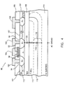
- a SOI-bulk CMOS compatible architecture according to the invention is shown in Figure 3 .
- the SOI-bulk well CMOS generally indicated by the numeral 50, comprises an N-channel MOSFET 52 and a P-channel MOSFET 54 formed above a buried silicon oxide layer 56.
- the buried oxide layer (BOX) 56 is formed on a silicon substrate 80.
- Surrounding the MOSFETs 52 and 54 is a field oxide region 58 (FOX).
- the N-channel MOSFET 52 includes a polycrystalline silicon gate 60, a N + source region 62 and a N + drain region 64. Between the source region 62 and the drain region 64, and below the gate 60, a P - region 66 is provided. In Fig. 3 , the source region 62 and the drain region 64 are shown to be shallower than the buried oxide layer, but in practice, the source region 62 and the drain region 64 may extend down to the buried oxide layer, as shown in Figure 4 . Located below the buried oxide layer 56 and below the P - region 66 is a region 67 which is of the same conductivity type i.e. P as the channel region 66.
- the region 67 is part of a P-well 68 which is formed above and below i.e. divided by the buried oxide layer 56.
- the P-channel MOSFET 54 includes a polycrystalline silicon gate 70, a P + source region 72 and a P + drain region 74. Between the source region 72 and the drain region 74, and below the gate 70, an N- region 76 is provided.
- the source region 72 and the drain region 74 are shown to be shallower than the buried oxide layer 56, but in practice, the source region 72 and the drain region 74 may extend down to the buried oxide layer 56 as shown in Figure 4 .
- a region 77 which is of the same conductivity type i.e. N as the channel region 76.
- the region 77 is part of an N-well 78 which is formed above and below i.e. divided by the buried oxide layer 56.
- gates may be metal, polycide or salicide.
- the wells 68 and 78 are implanted both above the buried oxide layer 56 and below the buried oxide layer 56 in the bulk region.
- the bulk region is an N, or P, substrate 80.
- One or more energy levels may be used for the ion implant of the wells 68, 78 after the buried oxide layer 56 is formed. In this regard, implant energies of 500 keV to several megavolts may be used.
- the wells 68, 78 may be formed using normal 100 keV or less implant energies followed by heavy oxygen implant for the formation of the buried oxide layer 56 using the SIMOX technique.
- the well drive then takes place during the oxygen implant anneal at approximately 1300 degrees C.
- the architecture in Figure 3 results in the reduction of parasitic junction capacitance under either N-channel or P-channel transistors. That is, if an N-substrate is used, the P-well will be junction isolated, that is, it will "float" electrically at approximately zero volts.
- a depletion zone will form between the P-well 68 and the substrate 80, which will serve to reduce charge transfer from all displacement current from electrode signals above it, eg. N + junctions 62, 64 and respective interconnects. The depletion zone and its effects are discussed in more detail below with reference to Figure 4 .
- Figure 4 shows the resistances, capacitances and the depletion zone formed under an N-channel MOSFET in the architecture according to the invention.
- the N-channel MOSFET generally indicated by the numeral 90 includes a polycrystalline silicon gate 92, a N + source region 94, and a N + drain region 96. Between the source region 94 and the drain region 96, and below the gate 92, a P - body region 98 is provided. Electrical contact to the source region 94, the gate region 96 and the gate 92, is made respectively by a metal source electrode 100, a metal drain electrode 102, and a metal gate electrode 104, which penetrate through an interoxide layer 105. Also provided is a metal P-well contact electrode 106.
- a field oxide layer 107 Surrounding the various semiconductor regions below the interoxide layer 105 is a field oxide layer 107. Also as before, a buried oxide layer 108 is present below the P - body region 98. Located below the buried oxide layer 108 and below the P - body region 98 is a region 112, which is of the same conductivity type i.e. P as the channel region 98. In the illustrated MOSFET 90, the region 110 is part of a P- well 112 which is formed above and below i.e. divided by the buried oxide layer 108. The P-well is formed in an N type substrate 114 using a bulk CMOS P-well mask as described with reference to Figure 3 .
- a depletion zone 116 forms between the P-well 112 and the N-substrate 114, which serves to reduce charge transfer due to displacement current induced in the substrate 114 by electrode signals applied to the N + regions 94, 96, and interconnect 106. Since active devices are not placed in the P-well 112, below the buried oxide layer 108, the doping levels of the P-well 112 in this region, and of the substrate 114, may be very light, less than or approximately equal to 1.0E15 atoms/cc. This results in a depletion spread i.e. the size of the depletion zone 116 of approximately 1 ⁇ m, or greater, for very lightly doped P-well/N-substrate junctions.
- the SOI configuration of the invention is easily adaptable and manufacturable from existing bulk CMOS configurations, while retaining the advantages of prior art SOI configurations. It may also be desirable, in the SOI configuration of the invention, to ohmically contact the wells beneath the buried oxide layer. This can be accomplished, with some increase in process complexity, by the use of a separate mask which is generated from the existing bulk CMOS mask database. The mask is generated by doing the following logical AND and OR functions on the existing CMOS layers:
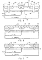
- a layer of photoresist 134 is deposited on the silicon layer 132.
- the photoresist layer 134 is exposed using the mask generated by the logical function c) above, and developed to define holes 136 in the photoresist layer 134.
- a silicon dioxide etch is used to form the upper portions of contact holes 138 in field oxide areas 130; then a silicon etch is used to form the intermediate portions of contact holes 138.
- the silicon etch will normally stop on the buried oxide layer 133, and it is then necessary to switch to a plasma etch gas to etch through the buried oxide layer 133.
- the contact plugs are formed of polycrystalline silicon (polysilicon) which is deposited onto the silicon layer 132 and into the contact plug holes 138 by means of chemical vapor deposition (CVD).
- the deposited polysilicon is indicated in Fig. 6 by the numeral 144.
- the polysilicon 144 above the silicon 132 and above the field oxide 130 is removed using chemical mechanical polishing (CMP), to leave the structure shown in Figure 7 , with a polysilicon contact plug 146 penetrating the field oxide 130, the silicon layer 132 and the buried oxide layer 133 to contact the P-well 140, and a polysilicon contact plug 148 penetrating the field oxide 130, the silicon layer 132 and the buried oxide layer 133 to contact the N-substrate 142.
- the contact plugs 146 and 148 could be made of a refractory metal, but CVD polysilicon is preferred to eliminate contact barriers.
- the P-well 140 is shown to be already formed.
- the contact plugs 146 and 148 contact the silicon layer 132 above the buried oxide layer 133, thereby also correctly contacting the respective body regions for the N- and P-channel transistors yet to be formed in Figure 7 .
- the well 140 connected to V SS , but also the P-type body regions for all N-channel transistors.
- the N-substrate 142 connected to V DD , but also the N-type body regions for all P-channel transistors.
- the contact plugs will receive additional doping which will improve their conductivity and further facilitate ohmic contact with the underlying wells or substrate.
- the ohmic resistance of the contact plugs may be as high as the mega-ohm range and still be acceptable.
- the resistance of the plugs should be between approximately 100 ohms and 10,000 ohms. As well, leakage current is normally 1 ⁇ A or far less, this resistance range is acceptable.
- Figure 8 shows an N-channel MOSFET according to the invention, including well contact plugs, showing the well to substrate depletion spread and well to substrate capacitance.
- the MOSFET includes a polycrystalline well contact plug 150 which extends through the buried oxide layer 108 to contact the P-well 112 which underlies the buried oxide layer 108.
- the P-well 112 is lightly doped (less than or approximately equal to 1.0E15 atoms/cc), and is biased to the source voltage (V SS ) via the contact electrode 152.
- the substrate 114 is biased to the drain voltage (V DD )
- the light doping and the voltage bias (V SS to V DD ) results in a very small well-to-substrate capacitance 153, and a large (3 ⁇ m to 10 ⁇ m) depletion spread 154.
- SOI designs claims faster gate speed than bulk CMOS.
- the configuration of the invention improves SOI speed further by reducing parasitic capacitance loads between the active devices and the substrate material. Further, the configuration of the invention provides the means whereby existing bulk CMOS database tooling can be used to provide a SOI configuration, with the attendant advantages inherent in SOI of reduced parasitic capacitance, improved speed, and the elimination of alpha particle SRAM memory faults. Further, by reducing the parasitic capacitance using wells implanted below the buried oxide layer, thinner buried oxide layers can be used compared to conventional SOI, reducing the large SIMOX manufacturing costs. Device yield is improved because pin-holes formed in the buried oxide layer do not affect device performance as in conventional SOI, because of the underlying wells in the configuration of the invention.
Description
- The present invention relates to semiconductor device configurations and manufacturing processes. In particular, the invention relates to a silicon-on-insulator (SOI) configuration and manufacturing process which is compatible with existing bulk complementary metal oxide semiconductor (CMOS) device architectures.
-
US-A-5 359 219 discloses a silicon-on-insulator device and method of fabrication thereof A buried oxide layer is formed an N-type semiconductor substrate, and a P-type layer is formed below the buried oxide layer. After formation of field oxide regions, extending down to the buried oxide layer, respective N- and P-type wells are implanted between the field oxide regions. The wells extend below the buried oxide layer into the P-type layer and above the buried oxide layer between the field oxide regions. - IEEE Electron Device Letters, Vol. 17, No 3, 1 March 1996, et al entitled "High-Speed Performance of 0.35 µm CMOS Gates Fabricated on Low-Dose SIMOX Substrates with/without an N-well Underneath the Buried Oxide Layer" discloses the formation of an N-well in a P-type semiconductor substrate. The N-well extends beneath a buried oxide region. The drawings show that the field oxide (LOCOS) extends down to the buried oxide (BOX).
-
EP-A-0 694 977 discloses the formation of highly doped N- and P-wells below the buried oxide layer in a SOI semiconductor device. - Complementary metal oxide semiconductor (CMOS) devices that are produced in mass quantities are referred to as "bulk" CMOS, because they include a semiconductive bulk substrate on which active or passive circuit elements are disposed. Recently, silicon-on-insulator (also referred to as silicon-oxide-insulator) SOI CMOS devices have been introduced which consume less power than do bulk CMOS devices. SOI devices are characterized by a thin layer of insulative material (the so-called buried oxide layer, or "SOI") that is sandwiched between a bulk substrate and the circuit elements of the device. Typically, no other layers of material are interposed between the SOI and the bulk substrate. In an SOI CMOS- device, the circuit elements above the SOI are established by regions of a field oxide semiconductive layer which are doped as appropriate with N-type or P-type conductivity dopants. For example, for an N channel transistor, the field oxide layer will include a gate element disposed over a body region having a P-type dopant, with the body region being disposed between a source region and a drain region, each of which are doped with an N-type dopant. These devices provide an important advantage in many applications such as battery-powered mobile telephones and battery-powered laptop computers. Also, SOI CMOS devices advantageously operate at higher speeds than do bulk CMOS devices. SOI CMOS architecture eliminates inherent parasitic circuit elements in bulk CMOS due to junction capacitances between adjacent components. Also, CMOS circuits are very fast, due to the fact that the bulk capacitance is very small. SOI CMOS is also immune to latchup. Other problems surrounding the technology include the SOI floating-body effect. This particular problem has been addressed by others, by example, in a paper entitled "Suppression of the SOI Floating-body Effects by Linked-Body Device Structure", by W. Chen, et. al., 1996 Symposium on VLSI Technology Digest of Technical Papers.
- One of the obstacles facing the increased use of SOI CMOS architecture is the fact that there is an enormous economic design investment in modern VLSI integrated circuit (IC) products. Typically, standard SOI does not behave the same way as bulk CMOS because of the dielectric isolation, and bulk CMOS designs are thus generally not compatible with, or readily transferable to an SOI architecture. Product groups must decide whether to re-design circuits for SOI CMOS, even when the circuit functions adequately using bulk CMOS, especially since the fabrication facilities will not try to run any new technology without a baseline. Although the prior art teaches combination of bulk CMOS and SOI CMOS architecture, by example Chen et.al. teaches locating wells above the buried oxide layer, the prior art does not teach any layout compatibility between the two architectures nor does it teach placing wells below the buried oxide layer. Thus, a need is seen to exist to provide a SOI configuration which is compatible with current bulk CMOS architecture. Using a bulk CMOS database, it would then be possible to create products rapidly for SOI fabrication and technologies.
- Accordingly, it is a primary object of the present invention to provide a method for creating a SOI CMOS type device compatible with bulk CMOS.
- A related object of the present invention is to provide method for creating a SOI CMOS device compatible with bulk CMOS using a bulk CMOS physical layout data base.
- Still another object of the present invention is to provide an SOI CMOS device fabricated in accordance with the foregoing objects.
- According to the invention there is provided a method as claimed in claim 7 for creating a SOI CMOS type device compatible with bulk CMOS, which device as claimed in claim 1 is created using a bulk CMOS physical layout data base. The method comprises using the P-well and N-well masks used in fabrication of the bulk CMOS devices. The N-well and P-well regions are fabricated by implanting the appropriate dopants above and below the buried oxide layer to create the basic SOI CMOS structure. Particular modifications to the basic SOI CMOS structure include providing a mask for establishing ohmic contact with the wells below the buried oxide layer. This can be accomplished by the use of a separate mask which is generated from the existing bulk CMOS mask database. The mask is generated by doing the following logical AND and OR functions on the existing CMOS layers:
- a) SOURCE/DRAIN [AND] P+ [AND] P-WELL [AND] 1st CONTACT
- b) SOURCE/DRAIN [AND] N+ [AND] N-WELL [AND] 1st CONTACT
- c) a) [OR] b)
- Other features of the invention are disclosed or apparent in the section entitled "BEST MODE OF CARRYING OUT THE INVENTION."
- For a fuller understanding of the present invention, reference is made to the accompanying drawings in the following detailed description of the Best Mode of Carrying Out the Invention. In the drawings:
-
Figure 1 is a cross-sectional view of a prior art SOI configuration. -
Figure 2 is a cross-sectional view of a prior art bulk CMOS configuration. -
Figure 3 is a cross-sectional view of a SOI CMOS device and architecture according to the invention. -
Figure 4 is a cross-sectional view of a SOI CMOS device according to the invention, showing the well-to-substrate depletion spread and well-to-substrate capacitance. -
Figure 5 shows a step in a method of forming well contact plugs in a SOI CMOS device according to the invention. -
Figure 6 shows a subsequent step in the method of forming well contact plugs in a SOI CMOS device according to the invention. -
Figure 7 is a cross-sectional view of a SOI CMOS device according to the invention, including well contact plugs. -
Figure 8 is a cross-sectional view of a SOI CMOS device according to the invention, including well contact plugs, showing the well-to-substrate depletion spread and well-to-substrate capacitance. - Reference numbers refer to the same or equivalent parts of the present invention throughout the several figures of the drawing.
- As semiconductor devices and manufacturing techniques are well known in the art, in order to avoid confusion, while enabling those skilled in the art to practice the claimed invention, this specification omits many details with respect to known items.
-
Figure 1 shows a conventional SOI CMOS configuration. The SOI CMOS, generally indicated by thenumeral 10, comprises an N-channel MOSFET 12 and a P-channel MOSFET 14 formed above a buriedsilicon oxide layer 16. The buried oxide layer (BOX) 16 is formed on asilicon substrate 18. Surrounding theMOSFETs MOSFET polycrystalline silicon gate 22. Body region 24 is P-type doped for theN channel MOSFET 12, and body region 26 is N-type doped for the P-channel MOSFET 14. As will be appreciated fromFigure 1 , theMOSFETs BOX layer 16 and theFOX region 20, and are insulated from any conducting substrate by means of theBOX layer 16. As a result, latch-up problems are eliminated and leakage problems are minimized. -
Figure 2 shows a conventional bulk CMOS configuration. The bulk CMOS, generally indicated by the numeral 30, comprises an N-channel MOSFET 32 and a P-channel MOSFET 34. The N-channel MOSFET 32 is located in a P-well 36, and the P-channel MOSFET 34 is located in an N-well 38. The P- and N-wells are formed in an N or P-type bulk 40, typically by means of ion implant and well drive. Surrounding theMOSFETs MOSFET polycrystalline silicon gate 44. - When an electrical potential is applied to one of the
gates 22 of theSOI CMOS 10, an electrical potential is drawn in the body regions 24 and 26 relative to thesubstrate 18. SOI MOSFET body regions have a floating electrical potential unless intentionally connected using area consuming layout methods. This effect is not found in bulk CMOS, and many bulk CMOS designs depend on the MOSFET body regions having a known electrical potential whereas SOI MOSFET's body regions are isolated from the bulk silicon. Also, circuit design simulations for SOI CMOS are based on the assumption that the MOSFETs are isolated from the bulk silicon, and circuit design performance depends on the silicon behaving in the same way as the model. Standard SOI does not behave the same way as bulk CMOS because of the dielectric isolation, and bulk CMOS designs are thus generally not compatible with, or readily transferable, to an SOI architecture. - A SOI-bulk CMOS compatible architecture according to the invention is shown in
Figure 3 . The SOI-bulk well CMOS, generally indicated by the numeral 50, comprises an N-channel MOSFET 52 and a P-channel MOSFET 54 formed above a buriedsilicon oxide layer 56. The buried oxide layer (BOX) 56 is formed on asilicon substrate 80. Surrounding theMOSFETs - The N-
channel MOSFET 52 includes apolycrystalline silicon gate 60, a N+ source region 62 and a N+ drain region 64. Between thesource region 62 and thedrain region 64, and below thegate 60, a P- region 66 is provided. InFig. 3 , thesource region 62 and thedrain region 64 are shown to be shallower than the buried oxide layer, but in practice, thesource region 62 and thedrain region 64 may extend down to the buried oxide layer, as shown inFigure 4 . Located below the buriedoxide layer 56 and below the P- region 66 is aregion 67 which is of the same conductivity type i.e. P as thechannel region 66. In the illustratedMOSFET 52, theregion 67 is part of a P-well 68 which is formed above and below i.e. divided by the buriedoxide layer 56. Similarly, the P-channel MOSFET 54 includes apolycrystalline silicon gate 70, a P+ source region 72 and a P+ drain region 74. Between thesource region 72 and thedrain region 74, and below thegate 70, an N-region 76 is provided. Thesource region 72 and thedrain region 74 are shown to be shallower than the buriedoxide layer 56, but in practice, thesource region 72 and thedrain region 74 may extend down to the buriedoxide layer 56 as shown inFigure 4 . Located below the buriedoxide layer 56 and below the N-region 76 is aregion 77 which is of the same conductivity type i.e. N as thechannel region 76. In the illustratedMOSFET 54, theregion 77 is part of an N-well 78 which is formed above and below i.e. divided by the buriedoxide layer 56. It should be obvious to one skilled in the art, that other planar MOSFET designs can be applied into this well formation method e.g. gates may be metal, polycide or salicide. - By using the standard bulk CMOS P-well and N-well masks, the
wells oxide layer 56 and below the buriedoxide layer 56 in the bulk region. In the embodiment illustrated inFigure 3 , the bulk region is an N, or P,substrate 80. One or more energy levels may be used for the ion implant of thewells oxide layer 56 is formed. In this regard, implant energies of 500 keV to several megavolts may be used. Alternatively, thewells oxide layer 56 using the SIMOX technique. The well drive then takes place during the oxygen implant anneal at approximately 1300 degrees C. The architecture inFigure 3 results in the reduction of parasitic junction capacitance under either N-channel or P-channel transistors. That is, if an N-substrate is used, the P-well will be junction isolated, that is, it will "float" electrically at approximately zero volts. A depletion zone will form between the P-well 68 and thesubstrate 80, which will serve to reduce charge transfer from all displacement current from electrode signals above it, eg. N+ junctions 62, 64 and respective interconnects. The depletion zone and its effects are discussed in more detail below with reference toFigure 4 . -
Figure 4 shows the resistances, capacitances and the depletion zone formed under an N-channel MOSFET in the architecture according to the invention. As before, the N-channel MOSFET, generally indicated by the numeral 90 includes apolycrystalline silicon gate 92, a N+ source region 94, and a N+ drain region 96. Between thesource region 94 and thedrain region 96, and below thegate 92, a P- body region 98 is provided. Electrical contact to thesource region 94, thegate region 96 and thegate 92, is made respectively by ametal source electrode 100, ametal drain electrode 102, and ametal gate electrode 104, which penetrate through aninteroxide layer 105. Also provided is a metal P-well contact electrode 106. Surrounding the various semiconductor regions below theinteroxide layer 105 is afield oxide layer 107. Also as before, a buriedoxide layer 108 is present below the P- body region 98. Located below the buriedoxide layer 108 and below the P- body region 98 is aregion 112, which is of the same conductivity type i.e. P as thechannel region 98. In the illustratedMOSFET 90, theregion 110 is part of a P- well 112 which is formed above and below i.e. divided by the buriedoxide layer 108. The P-well is formed in anN type substrate 114 using a bulk CMOS P-well mask as described with reference toFigure 3 . Adepletion zone 116 forms between the P-well 112 and the N-substrate 114, which serves to reduce charge transfer due to displacement current induced in thesubstrate 114 by electrode signals applied to the N+ regions 94, 96, andinterconnect 106. Since active devices are not placed in the P-well 112, below the buriedoxide layer 108, the doping levels of the P-well 112 in this region, and of thesubstrate 114, may be very light, less than or approximately equal to 1.0E15 atoms/cc. This results in a depletion spread i.e. the size of thedepletion zone 116 of approximately 1 µm, or greater, for very lightly doped P-well/N-substrate junctions. Thecapacitance 118 resulting from thedepletion zone 116, together with the buriedoxide layer capacitance 120, which are in series as shown, reduces the capacitance between theelectrodes substrate 114. - As discussed previously, existing bulk CMOS tooling is used in the SOI technique of the invention to form the N and P regions below the buried oxide layer shown in
Figures 3 and4 . As a result, the N-channel and P-channel transistors substrate contact 106, will be positioned correctly to ohmically contact their underlying device wells. Thus, the SOI configuration of the invention is easily adaptable and manufacturable from existing bulk CMOS configurations, while retaining the advantages of prior art SOI configurations. It may also be desirable, in the SOI configuration of the invention, to ohmically contact the wells beneath the buried oxide layer. This can be accomplished, with some increase in process complexity, by the use of a separate mask which is generated from the existing bulk CMOS mask database. The mask is generated by doing the following logical AND and OR functions on the existing CMOS layers: - a) SOURCE/DRAIN [AND] P+ [AND] P-WELL [AND] 1st CONTACT
- b) SOURCE/DRAIN [AND] N+ [AND] N-WELL [AND] 1st CONTACT
- c) a) [OR] b)
- As shown in
Figure 5 , after the formation offield oxide areas 130 in thesilicon layer 132 above the buriedoxide layer 133, a layer ofphotoresist 134 is deposited on thesilicon layer 132. Thephotoresist layer 134 is exposed using the mask generated by the logical function c) above, and developed to defineholes 136 in thephotoresist layer 134. Then, a silicon dioxide etch is used to form the upper portions ofcontact holes 138 infield oxide areas 130; then a silicon etch is used to form the intermediate portions of contact holes 138. The silicon etch will normally stop on the buriedoxide layer 133, and it is then necessary to switch to a plasma etch gas to etch through the buriedoxide layer 133. The plasma etch will stop on the bulk silicon (the P-well 140 or the N-substrate 142), thereby completing the formation of the contact holes 138. Since a low resistance ohmic contact is not necessary for the contact plugs, the contact plugs are formed of polycrystalline silicon (polysilicon) which is deposited onto thesilicon layer 132 and into the contact plug holes 138 by means of chemical vapor deposition (CVD). The deposited polysilicon is indicated inFig. 6 by the numeral 144. Thepolysilicon 144 above thesilicon 132 and above thefield oxide 130 is removed using chemical mechanical polishing (CMP), to leave the structure shown inFigure 7 , with apolysilicon contact plug 146 penetrating thefield oxide 130, thesilicon layer 132 and the buriedoxide layer 133 to contact the P-well 140, and apolysilicon contact plug 148 penetrating thefield oxide 130, thesilicon layer 132 and the buriedoxide layer 133 to contact the N-substrate 142. As an alternative to polysilicon, the contact plugs 146 and 148 could be made of a refractory metal, but CVD polysilicon is preferred to eliminate contact barriers. InFigures 5 to 7 , the P-well 140 is shown to be already formed. However, it is preferable to form the P-well (or N-well as the case may be) using MeV level implant energies after the formation of the contact plugs. This will result in the contact plugs having some implant doping embedded therein. This will facilitate ohmic contact through the plugs to the underlying wells. As can be seen fromFigure 7 , the contact plugs 146 and 148 contact thesilicon layer 132 above the buriedoxide layer 133, thereby also correctly contacting the respective body regions for the N- and P-channel transistors yet to be formed inFigure 7 . Thus, not only is the well 140 connected to VSS, but also the P-type body regions for all N-channel transistors. Likewise, not only is the N-substrate 142 connected to VDD, but also the N-type body regions for all P-channel transistors. - During the subsequent N+ and P+ source and drain region implant, the contact plugs will receive additional doping which will improve their conductivity and further facilitate ohmic contact with the underlying wells or substrate.
- It is important to note, however, that the wells below the buried oxide layer are only required to absorb reverse bias junction current leakage, and therefore, the ohmic resistance of the contact plugs may be as high as the mega-ohm range and still be acceptable. However, after undergoing the well doping and the source/drain doping as discussed above, the resistance of the plugs should be between approximately 100 ohms and 10,000 ohms. As well, leakage current is normally 1 µA or far less, this resistance range is acceptable.
-
Figure 8 shows an N-channel MOSFET according to the invention, including well contact plugs, showing the well to substrate depletion spread and well to substrate capacitance. - For purposes of conciseness, common reference numerals will be used for elements which are common to
Figures 4 and8 , and the discussion of these common elements above with reference toFigure 4 applies equally toFigure 8 . - As can be seen from
Figure 8 , the MOSFET includes a polycrystalline well contact plug 150 which extends through the buriedoxide layer 108 to contact the P-well 112 which underlies the buriedoxide layer 108. The P-well 112 is lightly doped (less than or approximately equal to 1.0E15 atoms/cc), and is biased to the source voltage (VSS) via thecontact electrode 152. Thesubstrate 114 is biased to the drain voltage (VDD) The light doping and the voltage bias (VSS to VDD) results in a very small well-to-substrate capacitance 153, and a large (3µm to 10µm)depletion spread 154. - SOI designs claims faster gate speed than bulk CMOS. The configuration of the invention improves SOI speed further by reducing parasitic capacitance loads between the active devices and the substrate material. Further, the configuration of the invention provides the means whereby existing bulk CMOS database tooling can be used to provide a SOI configuration, with the attendant advantages inherent in SOI of reduced parasitic capacitance, improved speed, and the elimination of alpha particle SRAM memory faults. Further, by reducing the parasitic capacitance using wells implanted below the buried oxide layer, thinner buried oxide layers can be used compared to conventional SOI, reducing the large SIMOX manufacturing costs. Device yield is improved because pin-holes formed in the buried oxide layer do not affect device performance as in conventional SOI, because of the underlying wells in the configuration of the invention.
Claims (16)
- A SOI CMOS device comprising:a P-channel CMOS transistor (54);an N-channel CMOS transistor (52);a first field oxide region (58) adjacent to the P-channel CMOS transistor (54);a second field oxide region (58) adjacent to the N-channel CMOS transistor (52);an electrically insulating layer (56) located below the P-channel transistor (54), the first field oxide region (58), the second field oxide region (58) and the N-channel CMOS transistor (52);an N-type semiconductor region (78) located above the electrically insulating layer (56) and extending below the first field oxide region (58);a P-type semiconductor region (68) located above the electrically insulating layer (56) and extending below the second field oxide region (58);a P-type semiconductor region (68) of a bulk semiconductor substrate (80) located directly below the electrically insulating layer (56), below the N-channel CMOS transistor (52), and the second field oxide region (58), and substantially in alignment with the P-type semiconductor region (68) located above the electrically insulating layer (56); andan N-type semiconductor region (78) of a bulk semiconductor substrate (80) located directly below the electrically insulating layer (56), below the P-channel CMOS transistor (54), and the first field oxide region (58), and substantially in alignment with the N-type semiconductor region (78) located above the electrically insulating layer (56).
- A SOI CMOS device as claimed in claim 1, wherein the P-type semiconductor region (68) is a P-well formed in a N-type bulk substrate.
- A SOI CMOS device as claimed in claim 1, wherein the N-type semiconductor region (78) is an N-well formed in a P-type bulk substrate.
- A SOI CMOS device as claimed in claim 1, wherein the N-type semiconductor region (78) is an N-well and the P-type semiconductor region (68) is a P-well.
- A SOI CMOS device as claimed in claim 4, wherein the N-well and the P-well are formed in a bulk semiconductor substrate (80) selected from the group consisting of: an undoped substrate, a P-type substrate and an N-type substrate.
- A SOI CMOS device as claimed in any preceding claim, further comprising a contact plug extending through the first field oxide region (58), the N-type semiconductor region (78) located above the electrically insulating layer (56), and the electrically insulating layer (56) to the N-type semiconductor region (78) located directly below the electrically insulating layer (56).
- A method of making a SOI CMOS device comprising the steps of:providing a bulk semiconductor substrate (80);providing a layer (56) of electrically insulating material above the substrate (80);providing a semiconductor device region above the layer of electrically insulating material (56);providing a first bulk CMOS fabrication mask for forming an N-type semiconductor region in the semiconductor substrate (80);forming an N-type semiconductor region (78) in the semiconductor substrate (80) above and below the electrically insulating layer (56) and removing said first mask;providing a second bulk CMOS fabrication mask for forming a P-type semiconductor region (68) in the semiconductor substrate (80);forming a P-type semiconductor region (68) in the substrate above and below the electrically insulating layer (56) and removing said mask;thereafter forming field oxide regions (58) between the N-type semiconductor region (78) and the P-type semiconductor region (68), the N-type and P-type semiconductor regions extending below the field oxide regions (58); andproviding a P-channel CMOS transistor (54) and an N-channel CMOS transistor (52) in the semiconductor device region.
- A method of making a SOI CMOS device as claimed in claim 7, wherein the step of forming a P-type semiconductor region (68) comprises the step of:forming a P-well in a N-type bulk substrate.
- A method of making a SOI CMOS device as claimed in claim 7, wherein the step of forming an N-type semiconductor region (78) comprises the step of:forming an N-well in a P-type bulk substrate.
- A method of making a SOI CMOS device as claimed in claim 7, wherein:the step of forming an N-type semiconductor region (78) comprises the step of forming an N-well in the bulk semiconductor substrate (80); andthe step of forming a P-type semiconductor region (68) comprises the step of forming a P-well in the semiconductor substrate (80).
- A method of making a SOI CMOS device as claimed in claim 10, wherein the bulk semiconductor substrate (80) is selected from the group consisting of: an undoped substrate, a P-type substrate and an N-type substrate.
- A method of making a SOI CMOS device as claimed in claim 7, further comprising the steps of:providing a third mask comprising a logical manipulation of a plurality of bulk CMOS fabrication masks, said third mask being used for forming ohmic contact with the N-type (78) and P-type (68) semiconductor regions formed in the bulk semiconductor substrate (80); andforming at least one ohmic contact structure contacting the N-type (78) and P-type (68) semiconductor regions formed in the semiconductor substrate.
- A method of making a SOI CMOS device as claimed in claim 12, wherein the at least one ohmic contact structure is formed by forming contact holes (138) and filling the contact holes (138) with polysilicon (144).
- A method of making a SOI CMOS device as claimed in claim 12 or claim 13, wherein the step of providing a third mask comprises:providing a mask created by logical manipulating of CMOS database expressions, namely:a) SOURCE/DRAIN [AND] P+ [AND] P-WELL [AND] 1st CONTACTb) SOURCE/DRAIN [AND] N+ [AND] N-WELL [AND] 1st CONTACTc) a) [OR] b).
- A method of making a SOI CMOS device as claimed in claim 12, 13 or 14, wherein:said step of forming at least one ohmic contact structure comprises forming ohmic contact structures for electrically contacting corresponding body regions of said P-channel (54) and N-channel (52) CMOS transistors, as well as said N-type (78) and P-type (68) semiconductor regions.
- A method of making a SOI CMOS device as claimed in any one of claims 13 to 15, wherein:said steps of forming an N-type semiconductor region (78) and forming a P-type semiconductor region (68) in the substrate (80) above and below the electrically insulating layer facilitates a step of improving device yield.
Applications Claiming Priority (3)
| Application Number | Priority Date | Filing Date | Title |
|---|---|---|---|
| US994355 | 1992-12-21 | ||
| US99435597A | 1997-12-19 | 1997-12-19 | |
| PCT/US1998/026846 WO1999033115A1 (en) | 1997-12-19 | 1998-12-18 | Silicon-on-insulator configuration which is compatible with bulk cmos architecture |
Publications (2)
| Publication Number | Publication Date |
|---|---|
| EP1042811A1 EP1042811A1 (en) | 2000-10-11 |
| EP1042811B1 true EP1042811B1 (en) | 2008-07-23 |
Family
ID=25540571
Family Applications (1)
| Application Number | Title | Priority Date | Filing Date |
|---|---|---|---|
| EP98964032A Expired - Lifetime EP1042811B1 (en) | 1997-12-19 | 1998-12-18 | Silicon-on-insulator configuration which is compatible with bulk cmos architecture |
Country Status (6)
| Country | Link |
|---|---|
| US (1) | US6215155B1 (en) |
| EP (1) | EP1042811B1 (en) |
| JP (1) | JP2001527293A (en) |
| KR (1) | KR100562539B1 (en) |
| DE (1) | DE69839780D1 (en) |
| WO (1) | WO1999033115A1 (en) |
Families Citing this family (43)
| Publication number | Priority date | Publication date | Assignee | Title |
|---|---|---|---|---|
| KR100259097B1 (en) * | 1998-04-02 | 2000-06-15 | 김영환 | Semiconductor device and method for fabricating the same |
| TW444266B (en) * | 1998-07-23 | 2001-07-01 | Canon Kk | Semiconductor substrate and method of producing same |
| US6274887B1 (en) | 1998-11-02 | 2001-08-14 | Semiconductor Energy Laboratory Co., Ltd. | Semiconductor device and manufacturing method therefor |
| US7141821B1 (en) * | 1998-11-10 | 2006-11-28 | Semiconductor Energy Laboratory Co., Ltd. | Semiconductor device having an impurity gradient in the impurity regions and method of manufacture |
| US6277679B1 (en) | 1998-11-25 | 2001-08-21 | Semiconductor Energy Laboratory Co., Ltd. | Method of manufacturing thin film transistor |
| JP3408762B2 (en) * | 1998-12-03 | 2003-05-19 | シャープ株式会社 | Semiconductor device having SOI structure and method of manufacturing the same |
| JP2001111056A (en) * | 1999-10-06 | 2001-04-20 | Mitsubishi Electric Corp | Semiconductor device and its manufacturing method |
| US6646287B1 (en) | 1999-11-19 | 2003-11-11 | Semiconductor Energy Laboratory Co., Ltd. | Semiconductor device with tapered gate and insulating film |
| US6287901B1 (en) * | 2000-01-05 | 2001-09-11 | International Business Machines Corporation | Method and semiconductor structure for implementing dual plane body contacts for silicon-on-insulator (SOI) transistors |
| US6429099B1 (en) * | 2000-01-05 | 2002-08-06 | International Business Machines Corporation | Implementing contacts for bodies of semiconductor-on-insulator transistors |
| TW476993B (en) * | 2000-01-19 | 2002-02-21 | Advanced Micro Devices Inc | Silicon on insulator circuit structure with buried semiconductor interconnect structure and method for forming same |
| JP3472742B2 (en) * | 2000-03-31 | 2003-12-02 | Necエレクトロニクス株式会社 | Semiconductor storage device |
| JP4776755B2 (en) | 2000-06-08 | 2011-09-21 | ルネサスエレクトロニクス株式会社 | Semiconductor device and manufacturing method thereof |
| TW501227B (en) | 2000-08-11 | 2002-09-01 | Samsung Electronics Co Ltd | SOI MOSFET having body contact for preventing floating body effect and method of fabricating the same |
| US6465331B1 (en) * | 2000-08-31 | 2002-10-15 | Micron Technology, Inc. | DRAM fabricated on a silicon-on-insulator (SOI) substrate having bi-level digit lines |
| JP2002076311A (en) * | 2000-09-01 | 2002-03-15 | Seiko Epson Corp | Semiconductor device and manufacturing method thereof |
| JP2002359310A (en) * | 2001-05-30 | 2002-12-13 | Matsushita Electric Ind Co Ltd | Semiconductor device and its fabricating method |
| KR100422468B1 (en) * | 2001-07-31 | 2004-03-11 | 삼성전자주식회사 | Soi element and soi product method |
| US6498371B1 (en) | 2001-07-31 | 2002-12-24 | Advanced Micro Devices, Inc. | Body-tied-to-body SOI CMOS inverter circuit |
| JP2003124345A (en) * | 2001-10-11 | 2003-04-25 | Oki Electric Ind Co Ltd | Semiconductor device and its manufacturing method |
| DE10151132A1 (en) * | 2001-10-17 | 2003-05-08 | Infineon Technologies Ag | Semiconductor structure with a component capacitively decoupled from the substrate |
| JP4176342B2 (en) * | 2001-10-29 | 2008-11-05 | 川崎マイクロエレクトロニクス株式会社 | Semiconductor device and layout method thereof |
| US6844224B2 (en) * | 2001-11-15 | 2005-01-18 | Freescale Semiconductor, Inc. | Substrate contact in SOI and method therefor |
| US20030134486A1 (en) * | 2002-01-16 | 2003-07-17 | Zhongze Wang | Semiconductor-on-insulator comprising integrated circuitry |
| US7432136B2 (en) | 2002-05-06 | 2008-10-07 | Advanced Micro Devices, Inc. | Transistors with controllable threshold voltages, and various methods of making and operating same |
| US7129142B2 (en) | 2002-06-11 | 2006-10-31 | Advanced Micro Devices, Inc. | Method of forming doped regions in the bulk substrate of an SOI substrate to control the operational characteristics of transistors formed thereabove, and an integrated circuit device comprising same |
| JP4850387B2 (en) * | 2002-12-09 | 2012-01-11 | ルネサスエレクトロニクス株式会社 | Semiconductor device |
| AU2004208199A1 (en) | 2003-01-30 | 2004-08-12 | X-Fab Semiconductor Foundries Ag | SOI structure comprising substrate contacts on both sides of the box, and method for the production of such a structure |
| JP4065855B2 (en) * | 2004-01-21 | 2008-03-26 | 株式会社日立製作所 | Biological and chemical sample inspection equipment |
| JP4664631B2 (en) * | 2004-08-05 | 2011-04-06 | 株式会社東芝 | Semiconductor device and manufacturing method thereof |
| US6949768B1 (en) * | 2004-10-18 | 2005-09-27 | International Business Machines Corporation | Planar substrate devices integrated with finfets and method of manufacture |
| US7244659B2 (en) * | 2005-03-10 | 2007-07-17 | Micron Technology, Inc. | Integrated circuits and methods of forming a field effect transistor |
| JPWO2007004535A1 (en) * | 2005-07-05 | 2009-01-29 | 株式会社ルネサステクノロジ | Semiconductor device and manufacturing method thereof |
| US20070023833A1 (en) * | 2005-07-28 | 2007-02-01 | Serguei Okhonin | Method for reading a memory cell having an electrically floating body transistor, and memory cell and array implementing same |
| US7696562B2 (en) * | 2006-04-28 | 2010-04-13 | Semiconductor Energy Laboratory Co., Ltd | Semiconductor device |
| US20070252233A1 (en) * | 2006-04-28 | 2007-11-01 | Semiconductor Energy Laboratory Co., Ltd. | Semiconductor device and method for manufacturing the semiconductor device |
| US7557002B2 (en) * | 2006-08-18 | 2009-07-07 | Micron Technology, Inc. | Methods of forming transistor devices |
| US7989322B2 (en) | 2007-02-07 | 2011-08-02 | Micron Technology, Inc. | Methods of forming transistors |
| JP6076224B2 (en) | 2013-09-05 | 2017-02-08 | ルネサスエレクトロニクス株式会社 | Semiconductor device and manufacturing method thereof |
| US9514987B1 (en) | 2015-06-19 | 2016-12-06 | International Business Machines Corporation | Backside contact to final substrate |
| US9837412B2 (en) * | 2015-12-09 | 2017-12-05 | Peregrine Semiconductor Corporation | S-contact for SOI |
| CN105680107B (en) * | 2016-03-16 | 2018-09-25 | 中国科学院上海微系统与信息技术研究所 | A kind of battery management chip circuit based on SOI technology |
| JP6889441B2 (en) | 2017-03-10 | 2021-06-18 | 三菱重工業株式会社 | Semiconductor device |
Family Cites Families (4)
| Publication number | Priority date | Publication date | Assignee | Title |
|---|---|---|---|---|
| US5463238A (en) * | 1992-02-25 | 1995-10-31 | Seiko Instruments Inc. | CMOS structure with parasitic channel prevention |
| US5359219A (en) * | 1992-12-04 | 1994-10-25 | Texas Instruments Incorporated | Silicon on insulator device comprising improved substrate doping |
| JPH0832040A (en) * | 1994-07-14 | 1996-02-02 | Nec Corp | Semiconductor device |
| JP3462301B2 (en) | 1995-06-16 | 2003-11-05 | 三菱電機株式会社 | Semiconductor device and manufacturing method thereof |
-
1998
- 1998-12-18 EP EP98964032A patent/EP1042811B1/en not_active Expired - Lifetime
- 1998-12-18 WO PCT/US1998/026846 patent/WO1999033115A1/en active IP Right Grant
- 1998-12-18 JP JP2000525929A patent/JP2001527293A/en active Pending
- 1998-12-18 KR KR1020007006811A patent/KR100562539B1/en not_active IP Right Cessation
- 1998-12-18 DE DE69839780T patent/DE69839780D1/en not_active Expired - Lifetime
-
1999
- 1999-10-18 US US09/420,605 patent/US6215155B1/en not_active Expired - Lifetime
Also Published As
| Publication number | Publication date |
|---|---|
| EP1042811A1 (en) | 2000-10-11 |
| WO1999033115A1 (en) | 1999-07-01 |
| US6215155B1 (en) | 2001-04-10 |
| DE69839780D1 (en) | 2008-09-04 |
| KR100562539B1 (en) | 2006-03-22 |
| KR20010033347A (en) | 2001-04-25 |
| JP2001527293A (en) | 2001-12-25 |
Similar Documents
| Publication | Publication Date | Title |
|---|---|---|
| EP1042811B1 (en) | Silicon-on-insulator configuration which is compatible with bulk cmos architecture | |
| US7968944B2 (en) | Integrated circuit chip with FETs having mixed body thicknesses and method of manufacture thereof | |
| EP0563879B1 (en) | Semiconductor memory device and method of fabricating the same | |
| US6815282B2 (en) | Silicon on insulator field effect transistor having shared body contact | |
| US8552500B2 (en) | Structure for CMOS ETSOI with multiple threshold voltages and active well bias capability | |
| US5105252A (en) | Low voltage BiCMOS and high voltage BiCMOS the same substrate | |
| US7078766B2 (en) | Transistor and logic circuit on thin silicon-on-insulator wafers based on gate induced drain leakage currents | |
| US20010025991A1 (en) | Silicon-on-insulator (SOI) substrate, method for fabricating SOI substrate and SOI mosfet using the SOI substrate | |
| US5170232A (en) | MOS field-effect transistor with sidewall spacers | |
| JPH05129429A (en) | Semiconductor device and manufacture thereof | |
| US6380598B1 (en) | Radiation hardened semiconductor memory | |
| WO2001043197A2 (en) | Source/drain-on-insulator (s/doi) field effect transistors and method of fabrication | |
| GB2281813A (en) | Integrated circuit with gate conductor defined resistor | |
| US8587062B2 (en) | Silicon on insulator (SOI) field effect transistors (FETs) with adjacent body contacts | |
| KR20010070479A (en) | Buried metal body contact structure and method for fabricating soi mosfet devices | |
| US6118155A (en) | Integrated ESD structures for use in ESD circuitry | |
| US6492209B1 (en) | Selectively thin silicon film for creating fully and partially depleted SOI on same wafer | |
| US5786265A (en) | Methods of forming integrated semiconductor devices having improved channel-stop regions therein, and devices formed thereby | |
| US20020112137A1 (en) | Partial trench body ties in sram cell | |
| US7355218B2 (en) | Semiconductor component with a MOS transistor | |
| JP3798659B2 (en) | Memory integrated circuit | |
| KR100344489B1 (en) | Manufacturing method of semiconductor integrated circuit device | |
| US20090269897A1 (en) | Methods of fabricating dual-depth trench isolation regions for a memory cell | |
| US6326247B1 (en) | Method of creating selectively thin silicon/oxide for making fully and partially depleted SOI on same waffer | |
| US6281550B1 (en) | Transistor and logic circuit of thin silicon-on-insulator wafers based on gate induced drain leakage currents |
Legal Events
| Date | Code | Title | Description |
|---|---|---|---|
| PUAI | Public reference made under article 153(3) epc to a published international application that has entered the european phase |
Free format text: ORIGINAL CODE: 0009012 |
|
| 17P | Request for examination filed |
Effective date: 20000710 |
|
| AK | Designated contracting states |
Kind code of ref document: A1 Designated state(s): DE FR GB NL |
|
| GRAP | Despatch of communication of intention to grant a patent |
Free format text: ORIGINAL CODE: EPIDOSNIGR1 |
|
| GRAS | Grant fee paid |
Free format text: ORIGINAL CODE: EPIDOSNIGR3 |
|
| GRAA | (expected) grant |
Free format text: ORIGINAL CODE: 0009210 |
|
| AK | Designated contracting states |
Kind code of ref document: B1 Designated state(s): DE FR GB NL |
|
| REG | Reference to a national code |
Ref country code: GB Ref legal event code: FG4D |
|
| REF | Corresponds to: |
Ref document number: 69839780 Country of ref document: DE Date of ref document: 20080904 Kind code of ref document: P |
|
| NLV1 | Nl: lapsed or annulled due to failure to fulfill the requirements of art. 29p and 29m of the patents act | ||
| PG25 | Lapsed in a contracting state [announced via postgrant information from national office to epo] |
Ref country code: NL Free format text: LAPSE BECAUSE OF FAILURE TO SUBMIT A TRANSLATION OF THE DESCRIPTION OR TO PAY THE FEE WITHIN THE PRESCRIBED TIME-LIMIT Effective date: 20080723 |
|
| PLBE | No opposition filed within time limit |
Free format text: ORIGINAL CODE: 0009261 |
|
| STAA | Information on the status of an ep patent application or granted ep patent |
Free format text: STATUS: NO OPPOSITION FILED WITHIN TIME LIMIT |
|
| 26N | No opposition filed |
Effective date: 20090424 |
|
| REG | Reference to a national code |
Ref country code: FR Ref legal event code: ST Effective date: 20090831 |
|
| REG | Reference to a national code |
Ref country code: GB Ref legal event code: 732E Free format text: REGISTERED BETWEEN 20091210 AND 20091216 |
|
| PG25 | Lapsed in a contracting state [announced via postgrant information from national office to epo] |
Ref country code: FR Free format text: LAPSE BECAUSE OF NON-PAYMENT OF DUE FEES Effective date: 20081231 |
|
| PGFP | Annual fee paid to national office [announced via postgrant information from national office to epo] |
Ref country code: GB Payment date: 20101123 Year of fee payment: 13 |
|
| PGFP | Annual fee paid to national office [announced via postgrant information from national office to epo] |
Ref country code: DE Payment date: 20101230 Year of fee payment: 13 |
|
| GBPC | Gb: european patent ceased through non-payment of renewal fee |
Effective date: 20111218 |
|
| PG25 | Lapsed in a contracting state [announced via postgrant information from national office to epo] |
Ref country code: GB Free format text: LAPSE BECAUSE OF NON-PAYMENT OF DUE FEES Effective date: 20111218 |
|
| REG | Reference to a national code |
Ref country code: DE Ref legal event code: R119 Ref document number: 69839780 Country of ref document: DE Effective date: 20130702 |
|
| PG25 | Lapsed in a contracting state [announced via postgrant information from national office to epo] |
Ref country code: DE Free format text: LAPSE BECAUSE OF NON-PAYMENT OF DUE FEES Effective date: 20130702 |