EP1039534A2 - Dynamic random access memory - Google Patents
Dynamic random access memory Download PDFInfo
- Publication number
- EP1039534A2 EP1039534A2 EP00103845A EP00103845A EP1039534A2 EP 1039534 A2 EP1039534 A2 EP 1039534A2 EP 00103845 A EP00103845 A EP 00103845A EP 00103845 A EP00103845 A EP 00103845A EP 1039534 A2 EP1039534 A2 EP 1039534A2
- Authority
- EP
- European Patent Office
- Prior art keywords
- semiconductor body
- recess
- portions
- over
- capacitor
- Prior art date
- Legal status (The legal status is an assumption and is not a legal conclusion. Google has not performed a legal analysis and makes no representation as to the accuracy of the status listed.)
- Withdrawn
Links
- 239000000463 material Substances 0.000 claims abstract description 102
- 239000004065 semiconductor Substances 0.000 claims abstract description 89
- 239000003990 capacitor Substances 0.000 claims abstract description 63
- 238000002955 isolation Methods 0.000 claims abstract description 22
- 238000000034 method Methods 0.000 claims abstract description 22
- 238000005530 etching Methods 0.000 claims abstract description 16
- 230000000873 masking effect Effects 0.000 claims abstract description 15
- 239000011810 insulating material Substances 0.000 claims abstract description 9
- 239000004020 conductor Substances 0.000 claims description 21
- 230000008878 coupling Effects 0.000 claims description 16
- 238000010168 coupling process Methods 0.000 claims description 16
- 238000005859 coupling reaction Methods 0.000 claims description 16
- 238000000151 deposition Methods 0.000 claims description 9
- 239000012212 insulator Substances 0.000 claims description 9
- 210000004027 cell Anatomy 0.000 description 23
- XUIMIQQOPSSXEZ-UHFFFAOYSA-N Silicon Chemical compound [Si] XUIMIQQOPSSXEZ-UHFFFAOYSA-N 0.000 description 15
- 229910052710 silicon Inorganic materials 0.000 description 15
- 239000010703 silicon Substances 0.000 description 15
- 229910021420 polycrystalline silicon Inorganic materials 0.000 description 12
- VYPSYNLAJGMNEJ-UHFFFAOYSA-N Silicium dioxide Chemical compound O=[Si]=O VYPSYNLAJGMNEJ-UHFFFAOYSA-N 0.000 description 10
- 238000003860 storage Methods 0.000 description 7
- 239000000758 substrate Substances 0.000 description 6
- 238000009792 diffusion process Methods 0.000 description 5
- 229920005591 polysilicon Polymers 0.000 description 5
- 239000000377 silicon dioxide Substances 0.000 description 5
- 235000012239 silicon dioxide Nutrition 0.000 description 5
- 238000004519 manufacturing process Methods 0.000 description 4
- 150000004767 nitrides Chemical class 0.000 description 4
- 230000000694 effects Effects 0.000 description 3
- 229910052581 Si3N4 Inorganic materials 0.000 description 2
- 230000015572 biosynthetic process Effects 0.000 description 2
- HQVNEWCFYHHQES-UHFFFAOYSA-N silicon nitride Chemical compound N12[Si]34N5[Si]62N3[Si]51N64 HQVNEWCFYHHQES-UHFFFAOYSA-N 0.000 description 2
- 210000000352 storage cell Anatomy 0.000 description 2
- BOTDANWDWHJENH-UHFFFAOYSA-N Tetraethyl orthosilicate Chemical compound CCO[Si](OCC)(OCC)OCC BOTDANWDWHJENH-UHFFFAOYSA-N 0.000 description 1
- 229910021417 amorphous silicon Inorganic materials 0.000 description 1
- 238000003491 array Methods 0.000 description 1
- 230000004888 barrier function Effects 0.000 description 1
- 239000013078 crystal Substances 0.000 description 1
- 230000008021 deposition Effects 0.000 description 1
- 238000010586 diagram Methods 0.000 description 1
- 238000009313 farming Methods 0.000 description 1
- 230000015654 memory Effects 0.000 description 1
- 239000002184 metal Substances 0.000 description 1
- 239000002210 silicon-based material Substances 0.000 description 1
- 125000006850 spacer group Chemical group 0.000 description 1
- 239000011800 void material Substances 0.000 description 1
Images





Classifications
-
- H—ELECTRICITY
- H10—SEMICONDUCTOR DEVICES; ELECTRIC SOLID-STATE DEVICES NOT OTHERWISE PROVIDED FOR
- H10B—ELECTRONIC MEMORY DEVICES
- H10B12/00—Dynamic random access memory [DRAM] devices
- H10B12/01—Manufacture or treatment
- H10B12/02—Manufacture or treatment for one transistor one-capacitor [1T-1C] memory cells
- H10B12/03—Making the capacitor or connections thereto
- H10B12/038—Making the capacitor or connections thereto the capacitor being in a trench in the substrate
- H10B12/0383—Making the capacitor or connections thereto the capacitor being in a trench in the substrate wherein the transistor is vertical
-
- G—PHYSICS
- G11—INFORMATION STORAGE
- G11C—STATIC STORES
- G11C11/00—Digital stores characterised by the use of particular electric or magnetic storage elements; Storage elements therefor
- G11C11/21—Digital stores characterised by the use of particular electric or magnetic storage elements; Storage elements therefor using electric elements
- G11C11/34—Digital stores characterised by the use of particular electric or magnetic storage elements; Storage elements therefor using electric elements using semiconductor devices
- G11C11/40—Digital stores characterised by the use of particular electric or magnetic storage elements; Storage elements therefor using electric elements using semiconductor devices using transistors
- G11C11/401—Digital stores characterised by the use of particular electric or magnetic storage elements; Storage elements therefor using electric elements using semiconductor devices using transistors forming cells needing refreshing or charge regeneration, i.e. dynamic cells
-
- H—ELECTRICITY
- H10—SEMICONDUCTOR DEVICES; ELECTRIC SOLID-STATE DEVICES NOT OTHERWISE PROVIDED FOR
- H10B—ELECTRONIC MEMORY DEVICES
- H10B12/00—Dynamic random access memory [DRAM] devices
- H10B12/01—Manufacture or treatment
- H10B12/02—Manufacture or treatment for one transistor one-capacitor [1T-1C] memory cells
- H10B12/03—Making the capacitor or connections thereto
- H10B12/038—Making the capacitor or connections thereto the capacitor being in a trench in the substrate
Definitions
- This invention relates generally to semiconductors and more particularly to dynamic random access memories (DRAMs).
- DRAMs dynamic random access memories
- DRAMs are made of storage cells having two main components: a storage capacitor; and, a transistor for enabling the transfer of charge to and from the capacitor.
- the capacitor is located in a deep trench which is etched into a semiconductor substrate. More particularly, the trench has a conductive material which provides a first electrode (i.e., sometimes referred to a the storage node) for the capacitor.
- the trench has a dielectric on its walls which provides the dielectric for the capacitor.
- a doped region in the substrate provides the second electrode for the capacitor.
- the first electrode is coupled to one of the source/drain regions of the cell's transistor through a coupling region formed in the semiconductor between an upper portion of the conductive region and a buried strap formed in the substrate.
- DRAM arrays are organized so that multiple storage cells are positioned as close as possible to one another.
- the transistor of one cell be electrically isolated from the transistor of an adjacent cell.
- These transistors are formed in active areas of the semiconductor substrate. These active areas are defined by a masking and etching process.
- One such process is sometimes referred to as shallow trench isolation (STI).
- STI shallow trench isolation
- a vertical area is etched into the electrically active silicon substrate and filled with oxide. This etching of the vertical area is typically performed using a mask which must be properly aligned with the trench capacitor. More particularly, as the mask becomes positioned closer to the transistor region, the resistance of the coupling region increases; whereas if the mask becomes positioned further from the transistor region of the cell, the likelihood that the active areas of two adjacent cells becoming electrically connected to one capacitor increases.
- a method including forming a trench capacitor in a semiconductor body.
- a recess is formed in the upper portion of the capacitor with such recess having sidewalls in the semiconductor body.
- a first material is deposited over the sidewalls and over a bottom of the recess.
- a second material is deposited over the first material.
- a mask is provided over the second material, such mask having: a masking region to cover one portion of said recess bottom; and a window over another portion of said recess bottom and over a portion of said recess sidewall, to expose underlying portions of the second material.
- Portions of the exposed underlying portions of the second material are removed while leaving substantially un-etched exposed underlying portions of the first material.
- the exposed portions of the first material and underlying portions of the semiconductor body are removed.
- An isolation region is formed in the removed portions of the semiconductor body.
- the mask is provided over the second material with a masking region covering one portion of said recess sidewall and one portion of said recess bottom and with a window disposed over an opposite portion of said recess sidewall and an opposite portion of said recess bottom to expose underlying portions of the second material.
- etching is provided into the exposed underlying portions of the semiconductor body to form a shallow trench in the semiconductor body; and, an insulating material is formed in the shallow trench to form a shallow trench isolation region.
- FIGS. 1 and 1A an exemplary one of an array of identical DRAM cells 8 in a semiconductor, here silicon body 16 is shown.
- Such exemplary DRAM cell 8 (FIG. 1A) has a partially vertical MOS transistor 9 electrically connected to a trench capacitor 10, both the MOS transistor 9 and the capacitor 10 being formed in an electrically isolated active area 11 of the semiconductor body 16.
- the source S of the MOS transistor 9 (here an N + doped region) is electrically connected to a BITLINE 17, the drain D of the MOS transistor 9 is electrically connected to one electrode 24 of the capacitor 10 through a conductive buried strap region 22.
- the carrier flow between the source S and the drain D of the transistor 9 is through a gate channel G, such carrier flow being controlled by a gate electrode, here the WORDLINE, as indicated.
- the WORDLINE is electrically insulated from a BITLINE by insulating cap 19.
- the gate electrode includes a doped polycrystalline silicon region 20 and a metal conductor 21 which provides the WORDLINE.
- the doped polycrystalline region 20 is electrically isolated from the capacitor electrode 24 by a dielectric 23.
- a second electrode for the capacitor 10 is provided by N + region 25 which is insulated from electrode 24 by insulator 14.
- the first upper portion 13 of the electrode 24 of capacitor 10 (i.e., a doped coupling region 13) is electrically coupled to the N + drain region D transistor 9 through a buried, conductive strap 22 in the semiconductor body 16 and an opposite, second upper portion of such capacitor 10 is disposed contiguous to an isolation region 28 defining a portion of the active area 11 having the transistor 9 of the cell 8.
- the trench capacitor 10, which is etched into a single crystal P type doped silicon substrate 16, has a conventional oxide collar 18, as shown.
- the lower portion, or level, of the trench 12 is here filled with an N + doped polycrystalline silicon (i.e., polysilicon) material 12 to provide the first electrode 24 of capacitor 10 and which is electrically isolated from a buried N + region second electrode 25 by an insulating node dielectric barrier, i.e., insulator 14.
- the storage node 24 of the capacitor 10 is typically formed from highly doped N + polysilicon and is connected to the drain region D of the transistor 9 through the self-aligned buried strap 22.
- the shallow trench isolation (STI) region 28 which isolates this cell 8 from adjacent cells in the array.
- an array of DRAM cells 8 is provided in the semiconductor body 16.
- Each one of such cells 8 has a transistor 9 in a corresponding electrically isolated active area 11 of the semiconductor body 16 and a capacitor 10 disposed in the trench 12 in such semiconductor body 16.
- a first upper portion, i.e., the coupling region 13, of the capacitor 10 i.e., the storage node 24
- the second electrode of the capacitor is provided by N + electrode region 25.
- the WORDLINE is insulated from the drain D, the coupling region 13 and the doped polysilicon 24 by the insulator 23.
- FIGS. 2 through 5, 5A through 10A, 5A' through 8A', 5B through 9B, and 5A' through 9B' the method for forming cell 8 will be described with like elements and materials being designated with the same numerical designation as in FIG. 1.
- An array of trench capacitors 10, such as that described in FIG. 1, is formed in the semiconductor body 16, as shown in FIGS. 2 and 3, for an exemplary one of the capacitors 10.
- Each one of the capacitors 10 includes: the insulator 14 on lower sidewall portions thereof and the conductive material 24 (i.e., the storage node) disposed in the trench 12.
- the conductive material 24 extends to a surface of the body 16. It is noted that a layer 32 of silicon nitride, (i.e., a pad nitride) is on the semiconductor body 16, as indicated, and that here the doped polysilicon material 24 extends to the upper surface of the silicon nitride layer 32, as shown in FIGS. 2 and 3.
- a recess 36 is formed in the upper portions of the conductive material 24 (FIG. 3).
- the recess 36 has a bottom 38 below the surface of the semiconductor body 16 and sidewalls 40 in the semiconductor body 16.
- the bottom 38 is recessed 50-400 nm below the surface to form a void over the capacitor 10.
- the bottom 38 of the recess 36 must also be above the top of collar 18. It should be understood that other processing or deposition steps may follow which includes the formation of an insulating layer over the bottom 38.
- a thin dielectric layer 39 (FIG. 1) of silicon dioxide is then formed, here thermally grown, on the exposed silicon recess 36 portion of the sidewalls 40 which will be the gate channel G while a thicker layer of such silicon dioxide is thermally grown over the top of the doped polycrystalline silicon 24.
- the silicon dioxide layer 39 is thicker over the doped polycrystalline silicon 24 than over the portion of the silicon sidewall 40 where the gate channel G will be because the doping of the polycrystalline silicon 24 is greater than the doping on the sidewall 40 portion.
- the doping concentration of the doped polycrystalline silicon 24 is in the order of 2x10 19 to 5x10 19 per cm 3 whereas the doping concentration of the gate channel G is in the order of 2x10 17 per cm 3 . (It is noted that, for convenience, the dielectric layer 39 is not shown in the succeeding FIGS.)
- a first material 42 here a silicon material, such as for example, polycrystalline silicon or amorphous silicon, is deposited as a layer of uniform, predetermined thickness, over the surface of the semiconductor body 16 (more particularly on the surface of the nitride layer 32) and on the sidewalls 40 and the bottom 38 of the recess 36 with such first material 42 under-filling such recess 36.
- a second material 44 here an antireflection layer, oxide, polynitride, or oxynitride, is deposited over the first material 42 and fills the under-filled recess to form a substantially planar surface over the semiconductor body.
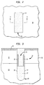
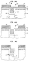
- a mask 46 is aligned with respect to the capacitor 10 over the planar surface with masking portions 48 of such mask 46 being disposed over the active area 11 and window, or opening, 50 in such mask 46 being disposed over isolation regions (i.e., over the body 16 where the STI regions 28 are to be formed) in the semiconductor body 16 between the active areas 11.
- the masking portions 48 cover one sidewall portion, here the left sidewall portion 40L in FIG. 5A of the recess 36 and the window 50 is disposed over an opposite sidewall portion, here sidewall portion 40R of the recess 36.
- An anisotropic etch is brought into contact with the mask 46 to selectively remove the exposed portions of the second material 44 (FIG. 6A) over the sidewall portion 40R of the recess. It is noted that the anisotropic etch removes portions of the second material 44 exposed by the window 50 disposed over the bottom portions of the recess to expose underlying portions of the first material 42 while leaving while leaving substantially un-etched exposed underlying portions of the first material 42.
- the etch used to remove the portions of the second material 44 exposed by window 50 here for example, well known oxide Reactive Ion Etch (RIE) selective to silicon (i.e., an oxide spacer type etch which etches silicon dioxide at a substantially higher rate than silicon) is selected so that it will not etch the first material 42, which is here silicon.
- RIE oxide Reactive Ion Etch
- etch here a reactive ion etch which etches the first material 42 without etching the second material 44 is used to selectively remove the exposed portions of the first material 42; (i.e., the portions 42a (FIG. 6A) of the first material 42 exposed by previously etching away portions of the second material 44, as described in FIG. 6A).
- the etching thereby exposes underlying portions of the semiconductor body 16 while leaving the bottom of the recess un-etched.
- semiconductor material is provided below the bottoms 38 to serve as the coupling region 13 (FIG. 1) for electrical connection to the buried strap 22 (FIG. 1) for the cell. It is noted that the coupling region 13 has a length, L.
- the exposed underlying portions of the semiconductor body is etched, here with a silicon RIE selective to oxide (i.e., an gate poly RIE etch which etches silicon at a significantly higher etch rate than silicon dioxide) and selective to the mask 48, again a vertical etching process to form a shallow trench 56 while leaving the bottom 38 of the recess un-etched to provide in the semiconductor material below the bottom of such recess for the coupling region 13 which maintains its length, L.
- a silicon RIE selective to oxide i.e., an gate poly RIE etch which etches silicon at a significantly higher etch rate than silicon dioxide
- an insulating material 60 for example TEOS, is formed in the shallow trench to form a shallow trench isolation (STI) region 28 thereby defining the active areas 11.
- STI shallow trench isolation
- layers 32 and 42 are removed, bitline diffusion 71 (FIG. 1) and node diffusion 72 (strap out-diffusion) are formed. These diffusions serve as the source-drain diffusions, here indicated by the N + drain D region in FIGS.
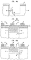
- FIGS. 5A' through 8A' corresponds to FIG. 5A except that the mask 46 in FIG. 5A is shifted to the left in FIG. 5A' and such left-shifted mask is designated as mask 46'.
- the window 50 in mask 46' is closer to sidewall 40L than mask 46 (FIG. 5A).
- the length, L, of the coupling region 13 remains unchanged. More particularly, the minimum length L of the coupling region 13 is defined by the length L' of the bottom 38 (FIG. 4) of the recess 36 minus the predetermined thickness of the first material 42 regardless of the misalignment of mask 46' as long as such misalignment still places the left edge of the window 50 at least to the right of the left sidewall 40L.
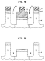
- FIG. 5 and FIGS. 5B through 9B the effect of the structure shown in FIG. 5 on the process described above in connection with FIGS. 5A-9A is shown. It is noted that the cross-sections shown in FIGS. 5B-9B are taken through line 5B-5B in FIG. 5.
- the recess 36 is formed in the upper portions of the conductive material 24 (FIG. 3) as shown in FIG. 4.
- the first material 40 is deposited as a layer of uniform, predetermined thickness, over the surface of the semiconductor body 16 (more particularly on the surface of the nitride layer 32) and on the sidewalls 40 and the bottom 38 of the recess 36 with such first material 42 under-filling such recess 36.
- the second material 44 is deposited over the first material 42 and fills the under-filled recess 36 to form a substantially planar surface over the semiconductor body 16.
- the mask 46 is aligned with respect to the capacitor 10 over the planar surface with masking portions 48 of such mask 46 disposed over the active areas and windows 50 in such mask 46 being disposed over the STI isolation regions to be formed in the semiconductor body 16 between the active areas 11 (FIG. 5). It is noted that the masking portions 48 cover one sidewall portion, here the left sidewall portion 40L in FIG. 5 of each one of the recesses 36 and the windows 50 are disposed over the remaining sidewall portion, here sidewall portions 40T, 40R, and 40B of each one of the recesses 36.
- the etch is brought into contact with the mask 46 to selectively remove the exposed portions of the second material 44 (FIG. 6B) over the sidewall portions 40T and 40B of each of the recesses. It is noted that the etch etches into portions of the second material 44 exposed by the windows 50 disposed over portions of each one of the recesses to expose underlying portions of the first material 42 while leaving substantially un-etched exposed underlying portions of the first material 42. Thus, the etch used to remove the portions of the second material 44 exposed by window 50 is selected so that it will not etch the first material 42, which is here silicon.
- another etch here a reactive ion etch which etches the first material 42 without etching the second material 44.
- the etch is used to selectively remove the exposed portions of the first material 42; (i.e., the portions 42a of the first material 42 exposed by etching away portions of the second material 44, as described in FIG. 6B) thereby exposing underlying portions of the semiconductor body 16.
- the exposed underlying portions of the semiconductor body 16 is etched, here with a silicon RIE, again a vertical etching process to form a shallow trench 56.
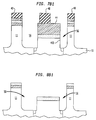
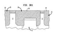
- FIG. 8B Next, referring to FIG. 9B, an insulating material 60 is formed in the shallow trench to form a shallow trench isolation (STI) region 28 being disposed in said second portion of the capacitor and defining the active areas 11.
- STI shallow trench isolation
- FIG. 5B' corresponds to FIG. 5B except that the mask 46 in FIG. 5B is shifted to the left in FIG. 5B' and such left-shifted mask is designated as mask 46'.
- the window 50 in mask 46' is closer to sidewall 40B than mask 46 (FIG. 5B').
- portions 42a of the first material are exposed.
- the exposed portions 42a are removed using the remaining, i.e., previously un-etched portions of the second material 44 as a mask.
- Etch also etches into the portions of the silicon body 16 under the portions 42a of the first layer, to produce the structure shown in FIG. 7B'.
- the remaining, exposed portions of the second material 44 are etched to produce the structure shown in FIG. 8B'.
- the insulating material 60 is deposited to form the STI regions 28 and thereby define the active areas 11.
Landscapes
- Engineering & Computer Science (AREA)
- Manufacturing & Machinery (AREA)
- Microelectronics & Electronic Packaging (AREA)
- Computer Hardware Design (AREA)
- Semiconductor Memories (AREA)
- Semiconductor Integrated Circuits (AREA)
Abstract
Description
Claims (7)
- A method, comprising:(a) forming a trench capacitor in a semiconductor body;(b) forming a recess in the upper portion of the capacitor with such recess having sidewalls in the semiconductor body;(c) depositing a first material over the sidewalls and over a bottom of the recess;(d) depositing a second material over the first material;(e) providing a mask over the second material, such mask having: a masking region to cover one portion of said recess bottom; and a window over a portion of said recess sidewall and another portion of said recess bottom to expose underlying portions of the second material;(f) selectively removing portions of the exposed underlying portions of the second material while leaving substantially un-etched exposed underlying portions of the first material;(g) selectively removing the exposed portions of the first material and underlying portions of the semiconductor body;(h) forming an isolation region in the removed portions of the semiconductor body.
- The method recited in claim 1 wherein the mask providing comprises:providing the mask over the second material with a masking region covering one portion of said recess sidewall and one portion of said recess bottom and with a window disposed over an opposite portion of said recess sidewall and an opposite portion of said recess bottom to expose underlying portions of the second material.
- The method recited in claim 1 wherein the forming an isolation region in the removed portions of the semiconductor body comprises:etching into the exposed underlying portions of the semiconductor body to form a shallow trench in the semiconductor body; andforming an insulating material in the shallow trench to form a shallow trench isolation region.
- A method, comprising:(a) forming a capacitor having a conductive material in a trench in a semiconductor body;(b) forming a recess in an upper portion of the conductive material with such recess having sidewalls in the semiconductor body;(c) depositing a first material over the surface of the semiconductor body and onto the sidewalls and a bottom of the recess with such first material under-filling such recess;(d) depositing a second material over the first material with such second material filling the under-filled recess;(e) forming a mask over the second material, such mask having an opening therein, the mask masking one portion of said recess sidewall and one portion of said recess bottom and the opening being disposed over an opposite portion of said recess sidewall and an opposite portion of said recess bottom to expose underlying portions of the second material;(f) selectively removing portions of the exposed underlying portions of the second material while leaving substantially un-etched exposed underlying portions of the first material;(g) selectively removing the exposed portions of the first material exposing underlying portions of the semiconductor body;(h) forming an isolation region in the exposed underlying portions of the semiconductor body.
- The method recited in claim 4 wherein the isolation region forming comprises:(a) etching into the exposed underlying portions of the semiconductor body to form a shallow trench in the semiconductor body; and(b) forming an insulating material into the shallow trench to form a shallow trench isolation region.
- A method for forming a DRAM cell in a semiconductor body, such cell having a transistor in an active area of the semiconductor body electrically connected to a capacitor disposed in a trench in such semiconductor body, a first upper portion of the capacitor being electrically coupled to the transistor and an opposite upper second portion of such capacitor being electrically isolated from the active area, comprising:(a) forming the capacitor in the trench of the semiconductor body, such capacitor having: an insulator on a lower sidewall portion thereof; and, a conductive material disposed in the trench, a lower portion of the conductive material being disposed on the insulator and an upper portion of the conductive material being disposed on the semiconductor body, such conductive material extending to a surface of the body;(b) forming a recess in the upper portion of the conductive material, such recess having a bottom below the surface of the semiconductor body and with sidewalls in the semiconductor body;(c) depositing a first material over the surface of the semiconductor body and onto the sidewalls and the bottom of the recess, with such first material under-filling such recess;(d) depositing a second material over the first material with such second material filling the under-filled recess forming a substantially planar surface over the semiconductor body;(e) forming a mask over the planar surface, such mask having an opening therein aligned with the capacitor to define the active area in the semiconductor body, the mask masking one portion of said recess sidewall and one portion of said recess bottom and the opening being disposed over an opposite portion of said recess sidewall and an opposite portion of said recess bottom to expose underlying portions of the second material;(f) selectively removing portions of the exposed underlying portions of the second material over said recess sidewall to expose underlying portions of the first material while leaving substantially un-etched exposed underlying portions of the first material;(g) selectively removing the exposed portions of the first material exposing underlying portions of the semiconductor body;(h) etching into the exposed underlying portions of the semiconductor body to form a shallow trench in the semiconductor body; and(i) forming an insulating material into the shallow trench to form a shallow trench isolation region defining the active region in said second upper portion of said capacitor with said opposite first portion of the capacitor being electrically connected to the transistor.
- A method for forming an array of DRAM cells in a semiconductor body, each one of such cells having a transistor in a corresponding electrically isolated active area of the semiconductor body and a capacitor disposed in a trench in such semiconductor body, a first portion of the capacitor being electrically coupled to the transistor and an opposite, second portion of such capacitor being disposed an isolation region defining a portion of the active area region having the transistor of such cell, such method, comprising:(a) forming an array of trench capacitors in a semiconductor body, each one of such capacitors having:an insulator on lower sidewall portions thereof and a conductive material disposed in the trench, a lower portion of the conductive material being disposed on the insulator and an upper portion of the conductive material being disposed on the semiconductor body, such conductive material extending to a surface of the body;(b) forming recesses in the upper portions of the conductive material, such recesses having bottoms below the surface of the semiconductor body and sidewalls in the semiconductor body;(c) depositing a first material over the surface of the semiconductor body and onto the sidewalls and the bottoms of the recesses with such first material under-filling such recesses;(d) depositing a second material over the first material and filling the under-filled recesses to form a substantially planar surface over the semiconductor body;(e) aligning a mask aver the planar surface with masking portions of such mask disposed over the active areas and windows in such mask being disposed over isolation regions in the semiconductor between the active areas, such masking portions covering one sidewall portion of the recesses and the windows being disposed over an opposite sidewall portion of the recesses;(f) selectively removing the exposed portions of the second material over the opposite sidewall portion of the recesses etching into portions of the second material exposed by the windows disposed over the bottom portions of each one of the recesses to expose underlying portions of the first material while leaving while leaving substantially un-etched exposed underlying portions of the first material;(g) selectively removing the exposed portions of the first material exposing underlying portions of the semiconductor body while leaving the bottoms of the recesses un-etched to provide in the semiconductor below the bottoms of such recesses a coupling region for each one of the cells;(h) etching into the exposed underlying portions of the semiconductor body to form a shallow trench while leaving the bottom of the recess un-etched to provide in the semiconductor below the bottom of such recesses the coupling region for each one of the cells; and(i) forming an insulating material into the shallow trench to form a shallow trench isolation region being disposed in said second portion of the capacitor and defining the active areas.
Applications Claiming Priority (2)
| Application Number | Priority Date | Filing Date | Title |
|---|---|---|---|
| US275337 | 1999-03-24 | ||
| US09/275,337 US6204140B1 (en) | 1999-03-24 | 1999-03-24 | Dynamic random access memory |
Publications (2)
| Publication Number | Publication Date |
|---|---|
| EP1039534A2 true EP1039534A2 (en) | 2000-09-27 |
| EP1039534A3 EP1039534A3 (en) | 2001-04-04 |
Family
ID=23051859
Family Applications (1)
| Application Number | Title | Priority Date | Filing Date |
|---|---|---|---|
| EP00103845A Withdrawn EP1039534A3 (en) | 1999-03-24 | 2000-02-24 | Dynamic random access memory |
Country Status (6)
| Country | Link |
|---|---|
| US (1) | US6204140B1 (en) |
| EP (1) | EP1039534A3 (en) |
| JP (1) | JP2000323684A (en) |
| KR (1) | KR100413277B1 (en) |
| CN (1) | CN1206721C (en) |
| TW (1) | TW477062B (en) |
Cited By (2)
| Publication number | Priority date | Publication date | Assignee | Title |
|---|---|---|---|---|
| WO2002047157A3 (en) * | 2000-12-06 | 2003-01-30 | Infineon Technologies Corp | Negative ion implant mask formation for self-aligned, sublithographic resolution patterning for single-sided verticle device formation |
| EP1553631A2 (en) * | 2004-01-09 | 2005-07-13 | International Business Machines Corporation | Nitrided STI liner oxide for reduced corner device impact on vertical device performance |
Families Citing this family (29)
| Publication number | Priority date | Publication date | Assignee | Title |
|---|---|---|---|---|
| DE19907174C1 (en) * | 1999-02-19 | 2000-09-14 | Siemens Ag | Method of manufacturing a DRAM cell with a trench capacitor |
| JP5172060B2 (en) * | 1999-09-17 | 2013-03-27 | インフィネオン テクノロジーズ アクチェンゲゼルシャフト | Self-aligned method for forming deep trenches in shallow trenches for semiconductor device isolation |
| TW429613B (en) * | 1999-10-21 | 2001-04-11 | Mosel Vitelic Inc | Dynamic random access memory with trench type capacitor |
| US6271080B1 (en) * | 1999-12-16 | 2001-08-07 | International Business Machines Corporation | Structure and method for planar MOSFET DRAM cell free of wordline gate conductor to storage trench overlay sensitivity |
| US6281539B1 (en) * | 2000-03-31 | 2001-08-28 | International Business Machines Corporation | Structure and process for 6F2 DT cell having vertical MOSFET and large storage capacitance |
| TW469635B (en) * | 2000-05-16 | 2001-12-21 | Nanya Technology Corp | Fabrication method of semiconductor memory cell transistor |
| US6284593B1 (en) * | 2000-11-03 | 2001-09-04 | International Business Machines Corporation | Method for shallow trench isolated, contacted well, vertical MOSFET DRAM |
| US6441422B1 (en) * | 2000-11-03 | 2002-08-27 | International Business Machines Corporation | Structure and method for ultra-scalable hybrid DRAM cell with contacted P-well |
| US6621112B2 (en) * | 2000-12-06 | 2003-09-16 | Infineon Technologies Ag | DRAM with vertical transistor and trench capacitor memory cells and methods of fabrication |
| JP2002289816A (en) * | 2001-03-23 | 2002-10-04 | Toshiba Corp | Semiconductor device and manufacturing method thereof |
| US6599798B2 (en) * | 2001-07-24 | 2003-07-29 | Infineon Technologies Ag | Method of preparing buried LOCOS collar in trench DRAMS |
| DE10208249B4 (en) * | 2002-02-26 | 2006-09-14 | Infineon Technologies Ag | Semiconductor memory with vertical selection transistor |
| US6605838B1 (en) * | 2002-09-30 | 2003-08-12 | International Business Machines Corporation | Process flow for thick isolation collar with reduced length |
| US6979851B2 (en) * | 2002-10-04 | 2005-12-27 | International Business Machines Corporation | Structure and method of vertical transistor DRAM cell having a low leakage buried strap |
| DE10254415A1 (en) * | 2002-11-21 | 2004-08-05 | Infineon Technologies Ag | Field effect transistor structure, associated semiconductor memory cell and associated manufacturing process |
| US6724031B1 (en) | 2003-01-13 | 2004-04-20 | International Business Machines Corporation | Method for preventing strap-to-strap punch through in vertical DRAMs |
| TW200425416A (en) * | 2003-05-02 | 2004-11-16 | Nanya Technology Corp | Self-alignment process in active area of memory cells with partial vertical channel |
| CN1317758C (en) * | 2003-05-23 | 2007-05-23 | 南亚科技股份有限公司 | Active Area Self-Alignment Process for Memory Cells with Partial Vertical Channels |
| TWI223442B (en) * | 2003-09-02 | 2004-11-01 | Nanya Technology Corp | DRAM cell array and its manufacturing method |
| KR100688056B1 (en) * | 2005-01-31 | 2007-03-02 | 주식회사 하이닉스반도체 | Semiconductor device having an omega gate and manufacturing method thereof |
| US20080048186A1 (en) * | 2006-03-30 | 2008-02-28 | International Business Machines Corporation | Design Structures Incorporating Semiconductor Device Structures with Self-Aligned Doped Regions |
| US7898014B2 (en) * | 2006-03-30 | 2011-03-01 | International Business Machines Corporation | Semiconductor device structures with self-aligned doped regions and methods for forming such semiconductor device structures |
| CN100466231C (en) * | 2006-04-24 | 2009-03-04 | 联华电子股份有限公司 | Trench capacitor DRAM device and method of making the same |
| TWI362744B (en) | 2008-04-14 | 2012-04-21 | Nanya Technology Corp | Dram and memory array |
| CN101582425B (en) * | 2008-05-12 | 2010-12-08 | 南亚科技股份有限公司 | Dynamic random access memory and memory array |
| KR101075490B1 (en) | 2009-01-30 | 2011-10-21 | 주식회사 하이닉스반도체 | Semiconductor device with buried gate and method for fabricating the same |
| US20130102123A1 (en) * | 2011-10-19 | 2013-04-25 | Nanya Technology Corporation | Method for fabricating single-sided buried strap in a semiconductor device |
| CN103377953A (en) * | 2012-04-27 | 2013-10-30 | 南亚科技股份有限公司 | Method for forming single-sided buried strap |
| US9842839B1 (en) * | 2017-01-12 | 2017-12-12 | Micron Technology, Inc. | Memory cell, an array of memory cells individually comprising a capacitor and a transistor with the array comprising rows of access lines and columns of digit lines, a 2T-1C memory cell, and methods of forming an array of capacitors and access transistors there-above |
Citations (2)
| Publication number | Priority date | Publication date | Assignee | Title |
|---|---|---|---|---|
| JPH10256498A (en) * | 1997-03-06 | 1998-09-25 | Toshiba Corp | Semiconductor memory device and method of manufacturing the same |
| EP1022782A2 (en) * | 1999-01-20 | 2000-07-26 | International Business Machines Corporation | Improved process for buried-strap self-aligned to deep storage trench |
Family Cites Families (14)
| Publication number | Priority date | Publication date | Assignee | Title |
|---|---|---|---|---|
| JPS61179571A (en) * | 1984-09-27 | 1986-08-12 | テキサス インスツルメンツ インコ−ポレイテツド | Memory cell and array thereof |
| US4830978A (en) * | 1987-03-16 | 1989-05-16 | Texas Instruments Incorporated | Dram cell and method |
| US5034787A (en) * | 1990-06-28 | 1991-07-23 | International Business Machines Corporation | Structure and fabrication method for a double trench memory cell device |
| US5198383A (en) * | 1991-06-25 | 1993-03-30 | Texas Instruments Incorporated | Method of fabricating a composed pillar transistor DRAM Cell |
| JP3301170B2 (en) * | 1993-08-09 | 2002-07-15 | ソニー株式会社 | Semiconductor device manufacturing method |
| US5360758A (en) * | 1993-12-03 | 1994-11-01 | International Business Machines Corporation | Self-aligned buried strap for trench type DRAM cells |
| US5543348A (en) * | 1995-03-29 | 1996-08-06 | Kabushiki Kaisha Toshiba | Controlled recrystallization of buried strap in a semiconductor memory device |
| US5827765A (en) * | 1996-02-22 | 1998-10-27 | Siemens Aktiengesellschaft | Buried-strap formation in a dram trench capacitor |
| US5717628A (en) * | 1996-03-04 | 1998-02-10 | Siemens Aktiengesellschaft | Nitride cap formation in a DRAM trench capacitor |
| US5905279A (en) * | 1996-04-09 | 1999-05-18 | Kabushiki Kaisha Toshiba | Low resistant trench fill for a semiconductor device |
| TW425718B (en) * | 1997-06-11 | 2001-03-11 | Siemens Ag | Vertical transistor |
| US5990511A (en) * | 1997-10-16 | 1999-11-23 | International Business Machines Corporation | Memory cell with transfer device node in selective polysilicon |
| US6066526A (en) * | 1998-01-22 | 2000-05-23 | International Business Machines Corporation | Method of making trench DRAM |
| US6074909A (en) * | 1998-07-31 | 2000-06-13 | Siemens Aktiengesellschaft | Apparatus and method for forming controlled deep trench top isolation layers |
-
1999
- 1999-03-24 US US09/275,337 patent/US6204140B1/en not_active Expired - Lifetime
-
2000
- 2000-02-24 EP EP00103845A patent/EP1039534A3/en not_active Withdrawn
- 2000-03-24 JP JP2000085406A patent/JP2000323684A/en not_active Withdrawn
- 2000-03-24 KR KR10-2000-0014994A patent/KR100413277B1/en not_active Expired - Fee Related
- 2000-03-24 CN CNB001047450A patent/CN1206721C/en not_active Expired - Fee Related
- 2000-06-26 TW TW089105345A patent/TW477062B/en not_active IP Right Cessation
Patent Citations (3)
| Publication number | Priority date | Publication date | Assignee | Title |
|---|---|---|---|---|
| JPH10256498A (en) * | 1997-03-06 | 1998-09-25 | Toshiba Corp | Semiconductor memory device and method of manufacturing the same |
| US6337241B1 (en) * | 1997-03-06 | 2002-01-08 | Kabushiki Kaisha Toshiba | Manufacturing method of a semiconductor memory device |
| EP1022782A2 (en) * | 1999-01-20 | 2000-07-26 | International Business Machines Corporation | Improved process for buried-strap self-aligned to deep storage trench |
Non-Patent Citations (1)
| Title |
|---|
| PATENT ABSTRACTS OF JAPAN * |
Cited By (2)
| Publication number | Priority date | Publication date | Assignee | Title |
|---|---|---|---|---|
| WO2002047157A3 (en) * | 2000-12-06 | 2003-01-30 | Infineon Technologies Corp | Negative ion implant mask formation for self-aligned, sublithographic resolution patterning for single-sided verticle device formation |
| EP1553631A2 (en) * | 2004-01-09 | 2005-07-13 | International Business Machines Corporation | Nitrided STI liner oxide for reduced corner device impact on vertical device performance |
Also Published As
| Publication number | Publication date |
|---|---|
| TW477062B (en) | 2002-02-21 |
| CN1206721C (en) | 2005-06-15 |
| CN1272688A (en) | 2000-11-08 |
| KR100413277B1 (en) | 2003-12-31 |
| KR20000063008A (en) | 2000-10-25 |
| JP2000323684A (en) | 2000-11-24 |
| EP1039534A3 (en) | 2001-04-04 |
| US6204140B1 (en) | 2001-03-20 |
Similar Documents
| Publication | Publication Date | Title |
|---|---|---|
| US6204140B1 (en) | Dynamic random access memory | |
| US5770484A (en) | Method of making silicon on insulator buried plate trench capacitor | |
| US5629226A (en) | Method of manufacturing a buried plate type DRAM having a widened trench structure | |
| US6440793B1 (en) | Vertical MOSFET | |
| US4830978A (en) | Dram cell and method | |
| KR100320332B1 (en) | Semiconductor device and manufacturing method thereof | |
| US6365452B1 (en) | DRAM cell having a vertical transistor and a capacitor formed on the sidewalls of a trench isolation | |
| US7449375B2 (en) | Fin semiconductor device and method for fabricating the same | |
| CA2130978C (en) | Self-aligned buried strap for trench type dram cells | |
| US5468670A (en) | Method for fabricating a semiconductor memory device having a stacked capacitor cell | |
| US6391705B1 (en) | Fabrication method of high-density semiconductor memory cell structure having a trench | |
| EP0690496A2 (en) | DRAM cell with trench capacitor | |
| US6255684B1 (en) | DRAM cell configuration and method for its production | |
| KR100445308B1 (en) | Memory with a trench capacitor and a selection transistor and method for producing the same | |
| KR100325472B1 (en) | Manufacturing Method of DRAM Memory Cells | |
| US5753551A (en) | Memory cell array with a self-aligned, buried bit line | |
| US5843819A (en) | Semiconductor memory device with trench capacitor and method for the production thereof | |
| US6414347B1 (en) | Vertical MOSFET | |
| US6541810B2 (en) | Modified vertical MOSFET and methods of formation thereof | |
| US6960503B2 (en) | Method for fabricating a trench capacitor | |
| KR100416607B1 (en) | Semiconductor device including transistor and manufacturing methode thereof | |
| US6902982B2 (en) | Trench capacitor and process for preventing parasitic leakage | |
| US6380027B2 (en) | Dual tox trench dram structures and process using V-groove | |
| US20050048711A1 (en) | Dynamic random access memory and fabrication thereof | |
| US6518613B2 (en) | Memory cell configuration with capacitor on opposite surface of substrate and method for fabricating the same |
Legal Events
| Date | Code | Title | Description |
|---|---|---|---|
| PUAI | Public reference made under article 153(3) epc to a published international application that has entered the european phase |
Free format text: ORIGINAL CODE: 0009012 |
|
| AK | Designated contracting states |
Kind code of ref document: A2 Designated state(s): DE FR GB IE IT NL |
|
| AX | Request for extension of the european patent |
Free format text: AL;LT;LV;MK;RO;SI |
|
| PUAL | Search report despatched |
Free format text: ORIGINAL CODE: 0009013 |
|
| AK | Designated contracting states |
Kind code of ref document: A3 Designated state(s): AT BE CH CY DE DK ES FI FR GB GR IE IT LI LU MC NL PT SE |
|
| AX | Request for extension of the european patent |
Free format text: AL;LT;LV;MK;RO;SI |
|
| 17P | Request for examination filed |
Effective date: 20010706 |
|
| AKX | Designation fees paid |
Free format text: DE FR GB IE IT NL |
|
| RAP1 | Party data changed (applicant data changed or rights of an application transferred) |
Owner name: INFINEON TECHNOLOGIES AG Owner name: INTERNATIONAL BUSINESS MACHINES CORPORATION |
|
| 17Q | First examination report despatched |
Effective date: 20061201 |
|
| STAA | Information on the status of an ep patent application or granted ep patent |
Free format text: STATUS: THE APPLICATION IS DEEMED TO BE WITHDRAWN |
|
| 18D | Application deemed to be withdrawn |
Effective date: 20090901 |