EP1037114A2 - Stage control method, exposure method, exposure apparatus and device manufacturing method - Google Patents
Stage control method, exposure method, exposure apparatus and device manufacturing method Download PDFInfo
- Publication number
- EP1037114A2 EP1037114A2 EP00301807A EP00301807A EP1037114A2 EP 1037114 A2 EP1037114 A2 EP 1037114A2 EP 00301807 A EP00301807 A EP 00301807A EP 00301807 A EP00301807 A EP 00301807A EP 1037114 A2 EP1037114 A2 EP 1037114A2
- Authority
- EP
- European Patent Office
- Prior art keywords
- stage
- substrate
- exposure
- predetermined velocity
- scanning direction
- Prior art date
- Legal status (The legal status is an assumption and is not a legal conclusion. Google has not performed a legal analysis and makes no representation as to the accuracy of the status listed.)
- Granted
Links
Images




Classifications
-
- G—PHYSICS
- G03—PHOTOGRAPHY; CINEMATOGRAPHY; ANALOGOUS TECHNIQUES USING WAVES OTHER THAN OPTICAL WAVES; ELECTROGRAPHY; HOLOGRAPHY
- G03F—PHOTOMECHANICAL PRODUCTION OF TEXTURED OR PATTERNED SURFACES, e.g. FOR PRINTING, FOR PROCESSING OF SEMICONDUCTOR DEVICES; MATERIALS THEREFOR; ORIGINALS THEREFOR; APPARATUS SPECIALLY ADAPTED THEREFOR
- G03F7/00—Photomechanical, e.g. photolithographic, production of textured or patterned surfaces, e.g. printing surfaces; Materials therefor, e.g. comprising photoresists; Apparatus specially adapted therefor
- G03F7/70—Microphotolithographic exposure; Apparatus therefor
- G03F7/70216—Mask projection systems
- G03F7/70358—Scanning exposure, i.e. relative movement of patterned beam and workpiece during imaging
-
- G—PHYSICS
- G03—PHOTOGRAPHY; CINEMATOGRAPHY; ANALOGOUS TECHNIQUES USING WAVES OTHER THAN OPTICAL WAVES; ELECTROGRAPHY; HOLOGRAPHY
- G03F—PHOTOMECHANICAL PRODUCTION OF TEXTURED OR PATTERNED SURFACES, e.g. FOR PRINTING, FOR PROCESSING OF SEMICONDUCTOR DEVICES; MATERIALS THEREFOR; ORIGINALS THEREFOR; APPARATUS SPECIALLY ADAPTED THEREFOR
- G03F7/00—Photomechanical, e.g. photolithographic, production of textured or patterned surfaces, e.g. printing surfaces; Materials therefor, e.g. comprising photoresists; Apparatus specially adapted therefor
- G03F7/70—Microphotolithographic exposure; Apparatus therefor
- G03F7/70691—Handling of masks or workpieces
- G03F7/70716—Stages
- G03F7/70725—Stages control
Definitions
- This invention relates to a method of controlling a stage in a stage apparatus that requires a high-speed, high-precision positioning capability. More particularly, the invention relates to the field of substrate scanning and exposure, and especially to a method of controlling the stage of a scanning exposure apparatus in which the pattern of a semiconductor or liquid crystal display elements is transferred to a substrate by photolithography. Further, the present invention falls under the category of exposure methods and apparatus as well as device manufacturing methods that utilize such a stage control method.
- a process for forming fine pattern on a device substrate in the manufacture of semiconductors and liquid crystal display devices generally utilizes a photolithography technique.
- An original pattern to undergo transfer is formed as a raised or recessed pattern on the light shielding surface of a glass substrate referred to as a reticle or mask.
- the pattern on this master plate exposed by illuminating light is projected for exposure onto a semiconductor wafer (referred to simply as a wafer below) or glass substrate for liquid crystal, which wafer or substrate has been coated with a photosensitive photoresist, via projection optics, whereby the latent image of the pattern is transferred to the resist.
- the substrate to be exposed is itself worked by carrying out etching in which the ratio of the selectivity of the worked surface to that of the resist image formed by developing is high.
- This exposure method employs a step-and-repeat scheme in which exposure areas (shot areas) obtained by subdividing a wafer are successively moved into an exposure field of the projection aligner optics and exposed to the pattern on the reticle after the wafer is positioned and stopped.
- This scheme scans the reticle and wafer synchronously with respect to the projection optics and performs exposure at the same time that the shot area is scanned relative to the exposure field.
- the reticle and wafer are adjusted to have a demaginification ratio that the projection optical system provides both longitudinally and transversely, whereby the reticle pattern is projected onto the wafer at the demagnification ratio.
- the scanning speed of the exposure area be controlled so as to be constant in order to control the amount of exposure to a prescribed amount in conformity with the properties and film thickness of the resist and in dependence upon the reticle pattern.
- the reticle and wafer must each attain a prescribed scanning speed before the reticle and the area to be exposed on the wafer enter the slit-shaped exposure area of the exposure apparatus.
- Figs. 10A and 10B illustrate the control sequence of a stage device holding a reticle or wafer.
- Fig. 10A illustrates the velocity profile (target velocity vs. time) of the stage
- Fig. 10 illustrates the acceleration profile (target acceleration vs. time) of the stage.
- elapsed time from start of scanning is plotted along the horizontal axis.
- the end time indicates time relating to one shot of exposure (shot processing time). Shot processing time is an important indicator that decides the processing time of one wafer.
- shot processing time is divided into five intervals. Stage operation will now be described in relation to these intervals.
- the stage is accelerated along the scanning direction from the at-rest position until it attains a target scanning velocity.
- This is acceleration time and corresponds to interval I.
- velocity is controlled in such a manner that a variation in synchronization will fall within tolerance.
- This is settling time and corresponds to interval II.
- the distance traveled by the stage during the total of acceleration time and settling time is referred to as the approach distance.
- the stage is then caused to travel at a constant velocity to perform exposure. This is exposure time and corresponds to interval III.
- the stage is allowed to travel for a time approximately equal to the settling time while the scanning velocity thereof is held constant. This is post-settling time and corresponds to interval IV. Deceleration of the stage then starts and the stage comes to rest with respect to the scanning direction. This is deceleration time and corresponds to interval V.
- the distance traveled by the stage during the total of post-settling time and deceleration time is referred to as the overrun distance.
- the approach distance and overrun distance are approximately equal.
- Another exposure method for the purpose of solving the aforementioned problems having a first step of accelerating a stage up to a predetermined velocity, the stage holding a substrate, a second step of transporting the stage at the predetermined velocity and exposing the substrate to a pattern, which has been formed on a master plate, during travel of the stage in a scanning direction, and a third step of stopping the stage traveling at the predetermined velocity, wherein the substrate being exposed to a plurality of the patterns by repeating the first through third steps, said exposure method comprises, wherein a position at which the stage is stopped by the third step is substantially the same as a starting position of the first step for exposing the substrate the next time.
- a further exposure method for the purpose of solving the aforementioned problems having a first step of accelerating a stage up to a predetermined velocity, the stage holding a substrate, a second step of transporting the stage at the predetermined velocity and exposing the substrate to a pattern, which has been formed on a master plate, during travel of the stage in a scanning direction, and a third step of stopping the stage traveling at the predetermined velocity, wherein the substrate being exposed to a plurality of the patterns by repeating the first through third steps, said exposure method comprises, wherein when, after the second step, the direction of movement of the stage in relation to the scanning direction thereof when the stage has been moved to a starting position of a subsequent first step coincides with the scanning direction of the stage in the second step when the next exposure is performed, a transition to the second step is made without stopping the stage at the starting position of the first step.
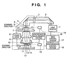
- Fig. 1 illustrates a step-and-scan exposure apparatus. Step-and-scan exposure in the Y direction will be taken as an example, with the longitudinal and transverse directions of the slit being taken as the X and Y directions, respectively.
- exposing light from a light source 1 has its illuminance and angle of incidence uniformalized and is converted to rectangular or arcuate slit light 4 in an illuminating system 2.
- the slit light impinges upon a reticle 5 on which a fine pattern has been formed.
- An ultra-high-voltage mercury vapor lamp or excimer laser is employed as the light source 1, though this does not impose a limitation upon the invention.
- the reticle 5 is held by a reticle stage 6.
- the slit light 4 passes through projection optics 9 and has its image formed as a slit light 14 in an exposure field on a plane that is optically a conjugate plane with respect to the pattern plane of reticle 5.
- control is carried out in such a manner that the exposure surface of a wafer 11 held by a wafer stage 12 will coincide with the exposure field.
- the reticle stage 6 and wafer stage 12 travel with respect to the projection optics 9 while synchronized so that the pattern is transferred to a photoresist layer on the wafer 11 by the slit light 14.
- a movable masking stage 3 is placed in the illuminating system 2 on a plane that is optically a conjugate plane with respect to the pattern plane of the reticle and travels relative to the optic axis of the illuminating system 2 while in sync with the reticle stage 6.
- the movable masking stage 3 has an aperture that defines a similar figure in terms of the optical magnification ratio so that only a predetermined exposure area of the reticle 5 will be exposed.
- the wafer 11 is shielded from the slit light in an area in which the exposure field deviates from the shot area, and hence the exposure of other shot areas can be prevented.
- the reticle stage 6 and wafer stage 12 are capable of having their position and velocity controlled in the Y direction, which is the scanning direction, with the former having its position controlled along X and ⁇ axes and the latter along six axes which include the Y axis.
- the movable masking stage 3 has its masking aperture controlled along two axes, namely along the X and Y directions.
- the actuators of all stages are non contact actuators such as linear motors and power is supplied from a stage drive system 8.
- the stage position measuring system includes XY ⁇ 3-axis interferometers (only the Y-axis interferometer is shown, namely an interferometer 19 for measurement of reticle position along the Y axis) on the side of reticle stage 6, XYZ ⁇ and tilt ( ⁇ x, ⁇ y) 6-axis interferometers (only the Y-axis interferometer is shown, namely an interferometer 15 for measurement of wafer position along the Y axis) on the side of wafer stage 12, and a focus sensor 10.
- the movable masking stage 3 has encoders (not shown) for four axes. These are controlled by a synchronous measurement system 18.
- a deviation representing a deviation in synchronization is calculated from measurement values obtained from the reticle interferometer 19 for Y measurement and from the wafer interferometer 15 for Y measurement, and the deviation in synchronization is corrected by making either the reticle stage 6 or wafer stage 12 the master and the other the slave.
- the deviation in synchronization is corrected by making the reticle stage 6 as slave and the wafer stage 12 as master, since a movement of the reticle stage 6 is more controllable than that of the wafer stage 12.
- Control of the reticle stage 6 and wafer stage 12 in the X and ⁇ directions also is performed in a manner similar to control in the Y direction.
- the reticle stage 6 is supported so as to lie substantially parallel to the travel reference plane of a reticle stage guide 7. As a result, the position of the reticle pattern plane is assured in the Z, ⁇ x and ⁇ y directions.
- the exposure plane of the wafer and the travel plane of the wafer stage are measured by the wafer focus sensor 10, and the wafer position is corrected by the wafer stage 12 in such a manner that the reticle pattern plane and wafer exposure plane, as well as the travel plane of the reticle stage and the travel plane of the wafer stage, will be situated as mutually conjugate planes via the projection optics.
- the above-described synchronous control and control for correcting the position of the wafer plane is carried out by a synchronous control system 16 situated at a rank superior to that of the stage drive system 8 and synchronous measurement system 18.
- a main control system 17 performs sequential control (control of the output of the light source, control changing wafers and reticles, etc.) other than synchronous control and delivers information concerning the running conditions of all stages (e.g., travel path, velocity and acceleration of the wafer stage 12) to the synchronous control system 16.
- the main control system 17, because of controlling the stage using velocity profiles described later, storages or sets the velocity profiles into a memory according to a layout of shot on the wafer 11.
- the stage position measurement system that provides the measurement reference and the reticle stage guide 7 that provides the position reference are fixed to a table (not shown) that holds the projection optics. In other words, measurement of position is carried out using the projection optics as a reference. Further, the wafer stage 12 is placed upon a wafer stage guide 13 supported by a vibration-proof mount (not shown).
- the positioning reference in the description to follow is the projection optics 9.
- the reticle stage 6 has already been positioned.
- the wafer 11 is delivered to the wafer stage 12 from a wafer transport system (not shown).
- the wafer 11 is subsequently controlled by the wafer stage 12.
- the position of the wafer 11 is detected by a wafer alignment system (not shown), and scanning exposure is carried out after the exposure field and the scanning starting position of a first exposure shot area on the wafer 11 are made to coincide.
- the wafer 11 is moved to the next shot area immediately and the wafer 11 is positioned at the starting position of the next scan, after which scanning exposure is repeated in similar fashion.
- the shot areas are arrayed as a two-dimensional grid on the wafer 11.
- the wafer is stepped in the Y direction to change the row of shots to be exposed. Exposure of this row then follows. By repeating this operation, the exposure of all shots is completed and the wafer is exchanged for a new wafer that is to undergo exposure.
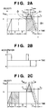
- Figs. 2A, 2B and 2C are diagrams useful in describing a first embodiment of a stage control method according to the present invention.
- Figs. 2A and 2B illustrate velocity and acceleration profiles, respectively, of the wafer stage 12, similar to the profile of Fig. 10A described earlier.
- Figs. 2A and 2B illustrate one shot scan from beginning to end.
- the scanning velocities V, accelerations/decelerations a, acceleration times Ta, settling times Ts and exposure times Tex are the same.
- the velocity profile of Fig. 10A has been added on in Fig. 2A.
- the maximum velocity of the stage in Fig. 2A is Vmax.
- the method of stage control according to the present invention differs from that of the prior art in that the velocity profile from the end of exposure to the stop of the wafer stage 12 is different.
- Fig. 10A which shows the conventional method of stage control
- travel of the stage continues for the post-settling time Ts at the velocity V even after the end of exposure, and then starting deceleraton, the stage comes to rest in deceleration time Ta.
- Fig. 2A showing the control method of the present invention, after exposure ends, the stage is accelerated over a maximum-acceleration time Taa, attains the maximum velocity Vmax, travels at the maximum velocity for a time Tvmax, then starts to be decelerated and returns to velocity V over a deceleration time Taa. The stage is decelerated further and then comes to rest.
- Td1 is a reduction time to be able to reduce processing time according to the present invention.
- Td1 (Vmax - V) ⁇ (Taa + Tvax)/V
- Td1 (1 - V/Vmax) ⁇ ⁇ Ts - (Vmax - V)/a ⁇
- Vmax at this time has an upper-limit value for satisfying Equations (1) to (5).
- Vmax ⁇ V ⁇ a ⁇ (Ts + V) ⁇ 0.5
- Vmax a ⁇ (Ta ⁇ (Ts + Ta) ⁇ 0.5
- Ta V/a
- the velocity profile in a case where Equation (6) is not satisfied is as shown in Fig. 2C.
- A1 is a triangle.
- Td1 can be calculated from Equation (5).
- stage control is not limited to the wafer stage; it can be applied to the reticle stage as well. Also, it can be applied to control of stage apparatus except an exposure apparatus.
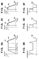
- Figs. 3A to 3F illustrate a second embodiment of a stage control method according to the present invention.
- stage travel is controlled in such a manner that acceleration applied to the stage before exposure and immediately after the end of exposure will vary continuously.
- Fig. 3A illustrates a velocity profile and Fig. 3B an acceleration profile.
- Figs. 3A and 3B illustrate profiles of one shot scan from beginning to end.
- the stage is accelerated in such a manner that its acceleration varies continuously until a target scanning velocity is attained (I'). Following the end of acceleration, velocity is controlled so that synchronous deviation will fall within tolerance (II'). Exposure is carried out while synchronous control is performed at the scanning velocity (III'). After exposure ends, the stage is accelerated in such a manner that acceleration varies continuously, then the stage is decelerated in such a manner that its deceleration varies continuously, and the stage is brought to rest (the solid line).
- the dashed line indicates the prior-art profile, namely the profile in a case where the stage is not accelerated after the end of exposure but is allowed to travel for the post-settling time, after which the stage is decelerated and stopped in such a manner that its acceleration varies continuously.
- area A2 (the ascending hatching) and area B2 (the descending hatching) may be calculated from known values in accordance with Equations (1) to (8).
- the change in acceleration it is not necessarily required for the change in acceleration to be continuous over the total overrun time. It is permissible, therefore, to shorten overrun time by making the change in acceleration continuous only in the deceleration region, as shown in Figs. 3C and 3D. Alternatively, the change may be made continuous only at the time of deceleration immediately before the stage comes to rest (Figs. 3E and 3F). In this case also the calculation method is the same as that described earlier.
- Control of stage travel in this embodiment suppresses a discontinuous change in acceleration. As a result, it is possible to reduce worse of positioning precision of the stage and distortion of the resist image, a decline in contrast and diminished durability of the stage itself caused by vibration produced by the stage during travel.
- Figs. 4A to 4C illustrate an exposure operation according to a third embodiment of the present invention.
- arrows indicate the amount of movement and direction thereof in step and scanning of an exposure field with respect to an exposure shot on a wafer.
- the double-line arrows indicate exposure scans.
- the arrows in these Figures express the path of the center position of the exposure field on the fixed side as viewed from the wafer on the side that actually moves.
- the exposure field has an effective length of greater than zero in the Y direction, i.e., the width in the transverse direction is greater than zero.
- Arrows indicative of the stepping operation are represented by bold lines, slender lines and broken lines.
- the bold lines represent the path when the present invention is applied and the broken lines represent the path in the case of the prior art.
- the fine lines indicate paths common to both cases.
- Fig. 4A illustrates a case where the Y stepping direction and the scanning direction immediately prior thereto are opposite when, while repeatedly reversing the shot scanning direction in the order of exposure, exposure of the same row of shots ends and a step in the Y direction is made to the next row of shots.
- the exposure field exposes a shot 51 by scanning exposure 54. This is followed by stepping movement in the X direction and simultaneous movement 55 for overrun in the Y direction, approach 56 until a prescribed scanning velocity is attained and then performing of scanning exposure 57.
- the XY stepping movement is carried out following the end of overrun 58.
- the process composed of the movements 58, 59 may be compared with the stepping movement 60 devoid of overrun, and whichever takes the shorter amount of time for movement may be selected.
- Another option is to select either one if the traveling times are equal. It will suffice if stepping time in the X direction in this embodiment is judged solely by a difference in the time for stepping movement in the Y direction because there is no difference in the traveling distance undergoing comparison.
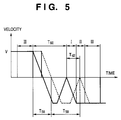
- Fig. 5 illustrates a Y-direction velocity profile of movements 58, 59 and 60.
- the positive Y direction is taken as the positive side of the velocity axis
- the movements 58, 59 are indicated by the dashed line
- the movement 60 is indicated by the solid line.
- the symbols employed in the first embodiment are used here as is. In this embodiment, however, the operation for accelerating the stage after scanning exposure set forth in the above-mentioned embodiment is not carried out in order to simplify the description.
- T58, T59, T60 represent the traveling times associated with the movements 58, 59, 60, respectively.
- Fig. 4B illustrates the operation of the present invention in a case where the Y stepping direction and the immediately preceding scanning direction are the opposite of each other.
- this embodiment is such that the stage is moved to the approach starting position of the next row of shots solely by movement 63 without the conventional overrun 61 and thereafter XY stepping movement 62.
- the Y stepping time may be compared and the movement 63 may be performed if it takes a shorter traveling time.
- wafer processing time is shortened in a manner similar to that of Fig. 4A.
- Fig. 4C shows an example of a case where the scanning directions of mutually adjacent shots that undergo successive exposure are the same.
- Such designation of shot traveling distance may be applied to the entire area of the wafer as a matter of course or to the shots on part of the wafer.
- this embodiment is such that the stage is moved to the approach starting position of the next shot solely by movement 68 without the movements 65, 65 that are required in the prior art.
- the Y stepping time may be compared and the movement that results in a shortening of the traveling time for the Y stepping time may be selected. In either case, wafer processing time can be shortened by a wide margin.
- the overrun operation may be omitted depending upon the case to thereby make possible an improvement in throughput.
- the velocity profile at stepping time is provided with only three types of travel, namely travel at uniform velocity, travel at uniform acceleration and travel at uniform deceleration.
- the present invention can be applied in similar fashion also in a case where stepping movement is performed in such a manner that acceleration will vary continuously.
- acceleration may be controlled continuously over part of the stepping movement, e.g., only immediately prior to the halting of stepping movement. This is similar to the foregoing embodiment.
- Fig. 6 illustrates an improvement on the stage control method of the embodiment described above.
- the Y stepping direction and the scanning direction immediately prior thereto are opposite when exposure of the same row of shots ends and a step in the Y direction is made to the next row of shots in a manner similar to that of Fig. 4A of the foregoing embodiment.
- the exposure field exposes a shot 51 by scanning exposure 54. This is followed by stepping movement in the X direction and simultaneous movement 55 for overrun in the Y direction, approach 56 until a prescribed scanning velocity is attained and then continuation of scanning exposure 57.
- Fig. 7 illustrates a Y-direction velocity profile of movements 60 and 70.
- the positive Y direction is taken as the positive side of the velocity axis
- the movement 60 is indicated by the dashed line
- the movement 70 is indicated by the solid line.
- the symbols employed in the first embodiment are used here as is. Further, in order to simplify the description, the acceleration of the stage after scanning exposure performed in the foregoing embodiment is not carried out in this embodiment.
- T70 represent the traveling time associated with movement 70.
- movement 70 makes it possible to arrive at the exposure starting position quicker, the extent of the shortening of time being equivalent to the time saved by not decelerating the stage. Consequently, as will be understood from Fig. 7, movement 70 makes it possible to shorten processing time by the length of time Ta in comparison with movement 60.
- the velocity profile at stepping time is provided with only three types of travel, namely travel at uniform velocity, travel at uniform acceleration and travel at uniform deceleration.
- the present invention can be applied in similar fashion also in a case where stepping movement is performed in such a manner that acceleration will vary continuously.
- acceleration may be controlled continuously over part of the stepping movement, e.g., only immediately prior to the halting of stepping movement. This is similar to the foregoing embodiment.
- the operation of the first and second embodiments for shortening overrun time by accelerating the stage after the end of scanning exposure is not carried out in order to simplify the description.
- such operation may be applied to this embodiment as well.
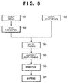
- Fig. 8 illustrates the flow of manufacture of a semiconductor device (a semiconductor chip such as an IC or LSI chip, a liquid crystal panel, a CCD, etc.).
- the circuit for the semiconductor device is designed at step 1 (circuit design).
- a mask on which the designed circuit pattern has been formed is fabricated at step 2 (mask fabrication).
- a wafer is manufactured using a material such as silicon or glass at step 3 (wafer manufacture).
- the actual circuit is formed on the wafer by lithography, using the mask and wafer that have been prepared, at step 4 (wafer process), which is also referred to as a "pre-process".
- a semiconductor chip is obtained, using the wafer fabricated at step 4, at step 5 (assembly), which is also referred to as a "post-process".
- This step includes steps such as actual assembly (dicing and bonding) and packaging (chip encapsulation).
- the semiconductor device fabricated at step 5 is subjected to inspections such as an operation verification test and durability test at step 6 (inspection).
- the semiconductor device is completed through these steps and then is shipped (step 7).
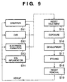
- Fig. 9 is a flowchart illustrating the detailed flow of the wafer process mentioned above.
- the surface of the wafer is oxidized at step 11 (oxidation).
- An insulating film is formed on the wafer surface at step 12 (CVD), electrodes are formed on the wafer by vapor deposition at step 13 (electrode formation), and ions are implanted in the wafer at step 14 (ion implantation).
- the wafer is coated with a photoresist at step 15 (resist treatment), the wafer is exposed to the circuit pattern of the mask to print the pattern onto the wafer by the above-described projection exposure apparatus at step 16 (exposure), and the exposed wafer is developed at step 17 (development). Portions other than the developed photoresist are etched away at step 18 (etching), and unnecessary resist left after etching is performed is removed at step 19 (resist removal). Multiple circuit patterns are formed on the wafer by implementing these steps repeatedly.
- a stage is accelerated before the stage is decelerated and stopped. This makes it possible to shorten the time for travel over the overrun distance.
- the stage is accelerated before the stage is decelerated and stopped. This makes it possible to shorten the time for travel over the overrun distance.
- a transition can be made to a second step without stopping the stage at the starting position of a first step. This makes it possible to improve throughput of the exposure apparatus.
Landscapes
- Physics & Mathematics (AREA)
- General Physics & Mathematics (AREA)
- Exposure And Positioning Against Photoresist Photosensitive Materials (AREA)
- Exposure Of Semiconductors, Excluding Electron Or Ion Beam Exposure (AREA)
- Container, Conveyance, Adherence, Positioning, Of Wafer (AREA)
Abstract
Description
and thus it can be determined that selection of
Claims (55)
- A stage control method characterized by comprising:a first step of accelerating a stage to a predetermined velocity;a second step of transporting the stage at the predetermined velocity; anda third step of decelerating and stopping the stage;said method having an acceleration step of accelerating the stage prior to the third step.
- The method according to claim 1, characterized in that said first to third steps are executed repeatedly and the stage is moved back and forth.
- The method according to claims 1 or 2, further characterized by comprising a calculation step of calculating acceleration time of the stage prior to said third step.
- The method according to any one of claims 1 to 3, characterized in that approach distance over which the stage attains the predetermined velocity from a rest position owing to said first step, and overrun distance over which the stage travels until it stops after execution of said second step, are approximately equal.
- The method according to any one of claims 1 to 4, characterized in that overrun distance over which the stage travels until it stops after execution of said second step, and approach distance necessary for the first step when the stage is driven the next time, are approximately equal.
- The method according to claim any one of claims 1 to 5, characterized in that acceleration of the stage at said first step is performed in such a manner that acceleration varies continuously.
- The method according to any one of claims 1 to 6, characterized in that deceleration of the stage at said third step is performed in such a manner that acceleration varies continuously.
- The method according to any one of claims 1 to 7, characterized in that acceleration of the stage prior to said third step is performed in such a manner that acceleration varies continuously.
- A stage control method characterized by comprising:a step of decelerating a stage transporting at a predetermined velocity; andan acceleration step of accelerating the stage prior to the deceleration step.
- The method according to claim 9, further characterized by comprising a calculation step of calculating acceleration time of the stage.
- The method according to claims 9 or 10, characterized in that a position of the stage stopped of said deceleration step, and an approach position of the stage for the next transporting at the predetermined velocity, are approximately equal.
- A stage control apparatus characterized by comprising:a stage which is capable of being moved;an actuator which drives the stage; anda control system controlling the actuator in accordance with profiles for accelerating the stage transporting at a predetermined velocity prior to a deceleration of the stage.
- The apparatus according to claim 12, characterized in that said control system has profiles for moving the stage back and forth.
- The apparatus according to claim 12 or 13, characterized in that said control system calculates acceleration time of the stage.
- The apparatus according to any one of claims 12 to 14, characterized in that approach distance over which the stage attains the predetermined velocity, and overrun distance over the stage after transporting at the predetermined velocity, are approximately equal.
- The apparatus according to any one of claims 12 to 15, characterized in that overrun distance over which the stage after transporting at the predetermined velocity, and approach distance for transporting the stage at the predetermined velocity the next time, are approximately equal.
- The apparatus according to any one of claims 12 to 16, characterized in that said control system has profiles for performing acceleration of the stage at the predetermined velocity in such a manner that acceleration varies continuously.
- The apparatus according to any one of claim 12 to 17, characterized in that said control system has profiles for performing deceleration of the stage at the predetermined velocity in such a manner that acceleration varies continuously.
- The apparatus according to any one of claims 12 to 18, characterized in that said control system has profiles for performing acceleration of the stage prior to deceleration of the stage in such a manner that acceleration varies continuously.
- A device manufacturing method characterized by comprising:an application step of applying a photosensitive agent to a substrate;an exposure step of exposing the substrate by an exposure method for scanningly moving a master plate having a pattern and a substrate exhibiting photosensitivity and projecting the pattern onto the substrate, said method including:a first step of accelerating a stage to a predetermined velocity, the stage holding the master plate or the substrate;a second step of transporting the stage at the predetermined velocity and exposing the substrate to the pattern during travel of the stage in a scanning direction; anda third step of stopping the stage traveling at the predetermined velocity; said method having an acceleration step of accelerating the stage prior to said third step;a step of developing the substrate that has been exposed; anda step of manufacturing a device from the exposed and developed substrate.
- The method according to claim 20, characterized in that said first to third steps are executed repeatedly and the stage is moved back and forth.
- The method according to claim 20 or 21, further characterized by comprising a calculation step of calculating acceleration time of the stage.
- The method according to any one of claims 20 to 22, characterized in that a distance over which the stage makes an approach run in the scanning direction until it attains the predetermined velocity from a rest position owing to said first step, and overrun distance over which the stage travels along the scanning direction until it stops after execution of said second step, are approximately equal.
- The method according to any one of claims 20 to 23, characterized in that overrun distance over which the stage travels until it stops after execution of said second step, and approach distance in the scanning direction necessary for the first step when the stage is driven the next time, are approximately equal.
- The method according to any one of claims 20 to 24, characterized in that the stage is a reticle stage holding a reticle having the pattern.
- The method according to any one of claims 20 to 24, characterized in that the stage is a substrate stage holding the substrate.
- The method according to claim 26, characterized in that the substrate stage is capable of being moved in a direction that perpendicularly intersects the scanning direction.
- The method according to claim 27, characterized in that said third step includes a moving step of moving the stage in the direction that perpendicularly intersects the scanning direction.
- The method according to claim 28, characterized in that a position at which the stage is stopped by said third step is approximately the same as a starting position of said first step for exposing the substrate the next time.
- The method according to any one of claims 20 to 29, characterized in that acceleration of the stage at said first step is performed in such a manner that acceleration varies continuously.
- The method according to any one of claims 20 to 30, characterized in that deceleration of the stage at said third step is performed in such a manner that acceleration varies continuously.
- The method according to any one of claims 20 to 31, characterized in that acceleration of the stage prior to said third step is performed in such a manner that acceleration varies continuously.
- A device manufacturing method characterized by comprising:an application step of applying a photosensitive agent to a substrate;an exposure step of exposing the substrate by an exposure method including:a first step of accelerating a stage to a predetermined velocity, the stage holding a substrate,a second step of transporting the stage at the predetermined velocity and exposing the substrate to a pattern, which has been formed on a master plate, during travel of the stage in a scanning direction, anda third step of stopping the stage traveling at the predetermined velocity, wherein the substrate being exposed to a plurality of the patterns by repeating said first through third steps, and wherein a position at which the stage is stopped by the third step is substantially the same as a starting position of the first step for exposing the substrate the next time;a step of developing the substrate that has been exposed; anda step of manufacturing a device from the exposed and developed substrate.
- The method according to claim 33, characterized in that the scanning direction of the stage in said second step is opposite the scanning direction which prevailed when exposure was performed previously.
- The method according to claim 33, characterized in that the scanning direction of the stage in said second step is identical with the scanning direction which prevailed when exposure was performed previously.
- A device manufacturing method characterized by comprising:an application step of applying a photosensitive agent to a substrate;an exposure step of exposing the substrate by an exposure method including:a first step of accelerating a stage to a predetermined velocity, the stage holding a substrate,a second step of transporting the stage at the predetermined velocity and exposing the substrate to a pattern, which has been formed on a master plate, during travel of the stage in a scanning direction, anda third step of stopping the stage traveling at the predetermined velocity, wherein the substrate being exposed to a plurality of the patterns by repeating said first through third steps, and wherein when, after said second step, the direction of movement of the stage in relation to the scanning direction thereof when the stage has been moved to a starting position of a subsequent first step coincides with the scanning direction of the stage in the second step when the next exposure is performed, a transition to the second step is made without stopping the stage at the starting position of said first step;a step of developing the substrate that has been exposed; anda step of manufacturing a device from the exposed and developed substrate.
- An exposure apparatus characterized by comprising:application means for applying a photosensitive agent to a substrate;exposure means for exposing the substrate by an exposure method for scanningly moving a master plate having a pattern and a substrate exhibiting photosensitivity and projecting the pattern onto the substrate, said method including:a first step of accelerating a stage to a predetermined velocity, the stage holding the master plate or the substrate;a second step of transporting the stage at the predetermined velocity and exposing the substrate to the pattern during travel of the stage in a scanning direction; anda third step of stopping the stage traveling at the predetermined velocity; said method having an acceleration step of accelerating the stage prior to said third stepmeans for developing the substrate that has been exposed.
- A stage control method characterized by comprising:a first step of accelerating a stage holding a substrate to a predetermined velocity;a second step of transporting the stage at the predetermined velocity and exposing the substrate to a pattern which has been formed on a master plate during travel of the stage in a scanning direction;a third step of decelerating and stopping the stage traveling at the predetermined velocity; anda comparison of comparing a step of moving a starting position of the next first step after an overrun operation of the second step in order to perform the third step, with a step of moving a starting position of the next first step without the overrun operation.
- The method according to claim 38, characterized in that a the substrate being exposed to a plurality of the patterns by repeating said first through third steps
- The method according to claim 38 or 39, further characterized by comprising a step of selecting any one of steps compared of the comparison step.
- The method according to claim 39, characterized in that the plurality of the patterns are arrayed a two-dimensional grid on the substrate.
- The method according to any one of claims 38 to 41, characterized in that the scanning direction of the stage in said second step is opposite the scanning direction which prevailed when exposure was performed previously.
- The method according to any one of claims 38 to 41, characterized in that the scanning direction of the stage in said second step is identical with the scanning direction which prevailed when exposure was performed previously.
- A stage control apparatus characterized by comprising:a stage which is capable of being moved;an actuator which drives the stage;exposure means for transporting the stage at the predetermined velocity and exposing the substrate to a pattern which has been formed on a master plate during travel of the stage in a scanning direction; anda control system, in order to perform decelerating and stopping the stage transporting at a predetermined velocity, for comparing a first profile with a second profile, and wherein the first profiles is used for moving a starting position of the next acceleration of the stage after an overrun operation performed by said exposure means and the second profile is used for moving a starting position of the next acceleration of the stage without the overrun operation.
- The apparatus according to claim 44, characterized in that said control system controls said exposure means to expose the substrate to a plurality of the patterns.
- The apparatus according to claim 44 or 45, characterized in that said control system selects either either the first profile or the second profile based on the comparing result.
- The apparatus according to claim 45, characterized in that the plurality of the patterns are arrayed a two-dimensional grid on the substrate.
- The apparatus according to any one of claims 44 to 47, characterized in that the scanning direction of the stage is opposite the scanning direction which prevailed when said exposure means performs exposure previously.
- The apparatus according to any one of claims 44 to 47, characterized in that the scanning direction of the stage is identical with the scanning direction which prevailed when said exposure means performs exposure previously.
- A device manufacturing method characterized by comprising:an application step of applying a photosensitive agent to a substrate to be held by a stage;a control step of controlling the stage by a stage control method including:a first step of accelerating a stage holding a substrate to a predetermined velocity;a second step of transporting the stage at the predetermined velocity and exposing the substrate to a pattern which has been formed on a master plate during travel of the stage in a scanning direction;a third step of decelerating and stopping the stage travelling at the predetermined velocity; anda comparison of comparing a step of moving a starting position of the next first step after an overrun operation of the second step in order to perform the third step, with a step of moving a starting position of the next first step without the overrun operation.a step of developing the substrate that has been exposed; anda step of manufacturing a device from the exposed and developed substrate.
- A stage control method for controlling a stage to perform a movement comprising:a first step of accelerating the stage to a predetermined velocity;a second step of transporting the stage at the predetermined velocity;a third step of further accelerating the stage from the predetermined velocity to a second, higher, velocity; anda fourth step of stopping the stage.
- A method according to claim 51, wherein the distance travelled by the stage during the first step is substantially equal to the total distance travelled by the stage during the third and fourth steps of the movement.
- A stage control apparatus, comprising:a movable stage;an actuator for moving the stage; andcontrol means for controlling the actuator, wherein the control means is operable to control the actuator to accelerate the stage to a first velocity, to move the stage a predetermined distance at first said velocity, to accelerate the stage to a second velocity higher than the first, and finally to decelerate the stage.
- An exposure apparatus for transferring a pattern from a mask to a substrate comprising:a movable stage for supporting the substrate;an actuator for moving the stage; andcontrol means operable to control the actuator to accelerate the stage to a first velocity, to move the stage a predetermined distance at said first velocity, to accelerate the stage to a second velocity higher than the first, and finally to decelerate the stage.
- A device manufacturing method comprising the steps of:transferring a pattern from a mask to a resist layer on a substrate, using an exposure apparatus according to claim 54;developing the resist layer on the substrate; andmanufacturing a device from the exposed and developed substrate.
Applications Claiming Priority (2)
| Application Number | Priority Date | Filing Date | Title |
|---|---|---|---|
| JP6153299 | 1999-03-09 | ||
| JP06153299A JP3796367B2 (en) | 1999-03-09 | 1999-03-09 | Stage control method, exposure method, exposure apparatus, and device manufacturing method |
Publications (3)
| Publication Number | Publication Date |
|---|---|
| EP1037114A2 true EP1037114A2 (en) | 2000-09-20 |
| EP1037114A3 EP1037114A3 (en) | 2003-07-16 |
| EP1037114B1 EP1037114B1 (en) | 2006-01-04 |
Family
ID=13173820
Family Applications (1)
| Application Number | Title | Priority Date | Filing Date |
|---|---|---|---|
| EP00301807A Revoked EP1037114B1 (en) | 1999-03-09 | 2000-03-06 | Stage control method, exposure method, exposure apparatus and device manufacturing method |
Country Status (5)
| Country | Link |
|---|---|
| US (1) | US6809798B1 (en) |
| EP (1) | EP1037114B1 (en) |
| JP (1) | JP3796367B2 (en) |
| KR (1) | KR100334852B1 (en) |
| DE (1) | DE60025306D1 (en) |
Cited By (2)
| Publication number | Priority date | Publication date | Assignee | Title |
|---|---|---|---|---|
| EP1422569A3 (en) * | 2002-11-20 | 2005-12-14 | ASML Holding N.V. | Movement control in a lithographic apparatus |
| CN113479353A (en) * | 2021-07-14 | 2021-10-08 | 贵州航天林泉电机有限公司 | Satellite turntable path planning method based on speed planning |
Families Citing this family (9)
| Publication number | Priority date | Publication date | Assignee | Title |
|---|---|---|---|---|
| JP4198334B2 (en) * | 2001-06-01 | 2008-12-17 | 富士通マイクロエレクトロニクス株式会社 | Processing method and apparatus using XY stage |
| JP4394500B2 (en) * | 2003-04-09 | 2010-01-06 | エーエスエムエル ネザーランズ ビー.ブイ. | Lithographic apparatus, device manufacturing method, and computer program |
| JPWO2005036620A1 (en) * | 2003-10-10 | 2006-12-28 | 株式会社ニコン | Exposure method, exposure apparatus, and device manufacturing method |
| KR100585108B1 (en) * | 2003-11-14 | 2006-06-01 | 삼성전자주식회사 | Wafer exposure method using a scanning exposure apparatus |
| US7016019B2 (en) * | 2003-12-16 | 2006-03-21 | Asml Netherlands B.V. | Lithographic apparatus and device manufacturing method |
| US20080148875A1 (en) * | 2006-12-20 | 2008-06-26 | Asml Netherlands B.V. | Inspection method and apparatus, lithographic apparatus, lithographic processing cell and device manufacturing method |
| TW201017340A (en) * | 2008-10-17 | 2010-05-01 | Nanya Technology Corp | Scanning exposure method |
| JP7301695B2 (en) * | 2019-09-19 | 2023-07-03 | キヤノン株式会社 | Control apparatus, control method, lithographic apparatus and method of manufacturing an article |
| JP7504168B2 (en) * | 2022-08-10 | 2024-06-21 | キヤノン株式会社 | Exposure apparatus, exposure method, and article manufacturing method |
Family Cites Families (10)
| Publication number | Priority date | Publication date | Assignee | Title |
|---|---|---|---|---|
| JP3234891B2 (en) * | 1990-10-30 | 2001-12-04 | 株式会社ニコン | Projection exposure equipment |
| US5343270A (en) * | 1990-10-30 | 1994-08-30 | Nikon Corporation | Projection exposure apparatus |
| US5617182A (en) | 1993-11-22 | 1997-04-01 | Nikon Corporation | Scanning exposure method |
| JP3451604B2 (en) * | 1994-06-17 | 2003-09-29 | 株式会社ニコン | Scanning exposure equipment |
| JPH0927443A (en) * | 1995-07-11 | 1997-01-28 | Nikon Corp | Stage drive controller |
| JPH09115825A (en) * | 1995-10-19 | 1997-05-02 | Nikon Corp | Scanning projection exposure equipment |
| DE69610691T2 (en) * | 1996-01-08 | 2001-05-03 | Canon K.K., Tokio/Tokyo | Exposure method and exposure device |
| US6260282B1 (en) * | 1998-03-27 | 2001-07-17 | Nikon Corporation | Stage control with reduced synchronization error and settling time |
| JP2000294479A (en) * | 1999-04-01 | 2000-10-20 | Canon Inc | Scanning exposure apparatus and device manufacturing method |
| US6285438B1 (en) * | 1999-05-19 | 2001-09-04 | Nikon Corporation | Scanning exposure method with reduced time between scans |
-
1999
- 1999-03-09 JP JP06153299A patent/JP3796367B2/en not_active Expired - Fee Related
-
2000
- 2000-03-06 EP EP00301807A patent/EP1037114B1/en not_active Revoked
- 2000-03-06 DE DE60025306T patent/DE60025306D1/en not_active Expired - Lifetime
- 2000-03-07 US US09/519,990 patent/US6809798B1/en not_active Expired - Fee Related
- 2000-03-09 KR KR1020000011908A patent/KR100334852B1/en not_active Expired - Fee Related
Cited By (4)
| Publication number | Priority date | Publication date | Assignee | Title |
|---|---|---|---|---|
| EP1422569A3 (en) * | 2002-11-20 | 2005-12-14 | ASML Holding N.V. | Movement control in a lithographic apparatus |
| US7389155B2 (en) | 2002-11-20 | 2008-06-17 | Asml Holding N.V. | Method and system for improved trajectory planning and execution |
| CN113479353A (en) * | 2021-07-14 | 2021-10-08 | 贵州航天林泉电机有限公司 | Satellite turntable path planning method based on speed planning |
| CN113479353B (en) * | 2021-07-14 | 2022-09-06 | 贵州航天林泉电机有限公司 | Satellite turntable path planning method based on speed planning |
Also Published As
| Publication number | Publication date |
|---|---|
| EP1037114B1 (en) | 2006-01-04 |
| JP3796367B2 (en) | 2006-07-12 |
| EP1037114A3 (en) | 2003-07-16 |
| US6809798B1 (en) | 2004-10-26 |
| JP2000260696A (en) | 2000-09-22 |
| KR100334852B1 (en) | 2002-05-03 |
| KR20000062808A (en) | 2000-10-25 |
| DE60025306D1 (en) | 2006-03-30 |
Similar Documents
| Publication | Publication Date | Title |
|---|---|---|
| US5933215A (en) | Exposure apparatus and device manufacturing method using the same | |
| US5917580A (en) | Scan exposure method and apparatus | |
| US6891175B2 (en) | Exposure apparatus and device manufacturing method using the same | |
| KR100975256B1 (en) | Exposure method, exposure apparatus, and method of manufacturing a device | |
| JPH088177A (en) | Projection exposure apparatus and device manufacturing method using the same | |
| US7154581B2 (en) | Scanning exposure apparatus, manufacturing method thereof, and device manufacturing method | |
| EP0834772B1 (en) | Exposure apparatus | |
| US6809798B1 (en) | Stage control method, exposure method, exposure apparatus and device manufacturing method | |
| US6641981B1 (en) | Exposure method, exposure apparatus, and device manufacturing method | |
| US6069683A (en) | Scanning exposure method and apparatus | |
| EP0833209B1 (en) | Scanning exposure apparatus and device manufacturing method using the same | |
| US6337734B1 (en) | Exposure control method, exposure apparatus and device manufacturing method | |
| US6172739B1 (en) | Exposure apparatus and method | |
| JP2009094256A (en) | Exposure method, exposure apparatus, and device manufacturing method | |
| JPH0917718A (en) | Exposure apparatus and device manufacturing method using the same | |
| JP4579367B2 (en) | Scanning exposure apparatus and scanning exposure method | |
| JP5607316B2 (en) | Exposure apparatus and device manufacturing method | |
| JP2003059806A (en) | Stage driving method, exposure method and exposure apparatus, and device manufacturing method | |
| JP2000077301A (en) | Exposure equipment | |
| JPH1126365A (en) | Projection exposure method and apparatus | |
| US6256085B1 (en) | Exposure apparatus | |
| KR20220014293A (en) | Exposing apparatus and method for manufacturing article | |
| JPH1092727A (en) | Projection exposure equipment | |
| JP2000164506A (en) | Exposure method and apparatus | |
| JPH1187233A (en) | Projection exposure equipment |
Legal Events
| Date | Code | Title | Description |
|---|---|---|---|
| PUAI | Public reference made under article 153(3) epc to a published international application that has entered the european phase |
Free format text: ORIGINAL CODE: 0009012 |
|
| AK | Designated contracting states |
Kind code of ref document: A2 Designated state(s): AT BE CH CY DE DK ES FI FR GB GR IE IT LI LU MC NL PT SE |
|
| AX | Request for extension of the european patent |
Free format text: AL;LT;LV;MK;RO;SI |
|
| PUAL | Search report despatched |
Free format text: ORIGINAL CODE: 0009013 |
|
| AK | Designated contracting states |
Designated state(s): AT BE CH CY DE DK ES FI FR GB GR IE IT LI LU MC NL PT SE |
|
| AX | Request for extension of the european patent |
Extension state: AL LT LV MK RO SI |
|
| 17P | Request for examination filed |
Effective date: 20031126 |
|
| AKX | Designation fees paid |
Designated state(s): DE GB NL |
|
| 17Q | First examination report despatched |
Effective date: 20040326 |
|
| GRAP | Despatch of communication of intention to grant a patent |
Free format text: ORIGINAL CODE: EPIDOSNIGR1 |
|
| GRAS | Grant fee paid |
Free format text: ORIGINAL CODE: EPIDOSNIGR3 |
|
| GRAA | (expected) grant |
Free format text: ORIGINAL CODE: 0009210 |
|
| AK | Designated contracting states |
Kind code of ref document: B1 Designated state(s): DE GB NL |
|
| PG25 | Lapsed in a contracting state [announced via postgrant information from national office to epo] |
Ref country code: NL Free format text: LAPSE BECAUSE OF FAILURE TO SUBMIT A TRANSLATION OF THE DESCRIPTION OR TO PAY THE FEE WITHIN THE PRESCRIBED TIME-LIMIT Effective date: 20060104 |
|
| REG | Reference to a national code |
Ref country code: GB Ref legal event code: FG4D |
|
| REF | Corresponds to: |
Ref document number: 60025306 Country of ref document: DE Date of ref document: 20060330 Kind code of ref document: P |
|
| PG25 | Lapsed in a contracting state [announced via postgrant information from national office to epo] |
Ref country code: DE Free format text: LAPSE BECAUSE OF FAILURE TO SUBMIT A TRANSLATION OF THE DESCRIPTION OR TO PAY THE FEE WITHIN THE PRESCRIBED TIME-LIMIT Effective date: 20060405 |
|
| NLV1 | Nl: lapsed or annulled due to failure to fulfill the requirements of art. 29p and 29m of the patents act | ||
| PLBI | Opposition filed |
Free format text: ORIGINAL CODE: 0009260 |
|
| 26 | Opposition filed |
Opponent name: ASML NETHERLANDS B.V. Effective date: 20061003 |
|
| PLAX | Notice of opposition and request to file observation + time limit sent |
Free format text: ORIGINAL CODE: EPIDOSNOBS2 |
|
| PLAF | Information modified related to communication of a notice of opposition and request to file observations + time limit |
Free format text: ORIGINAL CODE: EPIDOSCOBS2 |
|
| PLBB | Reply of patent proprietor to notice(s) of opposition received |
Free format text: ORIGINAL CODE: EPIDOSNOBS3 |
|
| PLBP | Opposition withdrawn |
Free format text: ORIGINAL CODE: 0009264 |
|
| RDAF | Communication despatched that patent is revoked |
Free format text: ORIGINAL CODE: EPIDOSNREV1 |
|
| REG | Reference to a national code |
Ref country code: DE Ref legal event code: R103 Ref document number: 60025306 Country of ref document: DE Ref country code: DE Ref legal event code: R064 Ref document number: 60025306 Country of ref document: DE |
|
| RDAG | Patent revoked |
Free format text: ORIGINAL CODE: 0009271 |
|
| STAA | Information on the status of an ep patent application or granted ep patent |
Free format text: STATUS: PATENT REVOKED |
|
| 27W | Patent revoked |
Effective date: 20110204 |
|
| GBPR | Gb: patent revoked under art. 102 of the ep convention designating the uk as contracting state |
Effective date: 20110204 |
|
| PGFP | Annual fee paid to national office [announced via postgrant information from national office to epo] |
Ref country code: GB Payment date: 20110311 Year of fee payment: 12 |