EP1035637A2 - Power supply system comprising capacitors connected switchably - Google Patents
Power supply system comprising capacitors connected switchably Download PDFInfo
- Publication number
- EP1035637A2 EP1035637A2 EP00301666A EP00301666A EP1035637A2 EP 1035637 A2 EP1035637 A2 EP 1035637A2 EP 00301666 A EP00301666 A EP 00301666A EP 00301666 A EP00301666 A EP 00301666A EP 1035637 A2 EP1035637 A2 EP 1035637A2
- Authority
- EP
- European Patent Office
- Prior art keywords
- capacitors
- series
- voltage
- power supply
- switching means
- Prior art date
- Legal status (The legal status is an assumption and is not a legal conclusion. Google has not performed a legal analysis and makes no representation as to the accuracy of the status listed.)
- Withdrawn
Links
Images


Classifications
-
- H—ELECTRICITY
- H02—GENERATION; CONVERSION OR DISTRIBUTION OF ELECTRIC POWER
- H02M—APPARATUS FOR CONVERSION BETWEEN AC AND AC, BETWEEN AC AND DC, OR BETWEEN DC AND DC, AND FOR USE WITH MAINS OR SIMILAR POWER SUPPLY SYSTEMS; CONVERSION OF DC OR AC INPUT POWER INTO SURGE OUTPUT POWER; CONTROL OR REGULATION THEREOF
- H02M3/00—Conversion of dc power input into dc power output
- H02M3/02—Conversion of dc power input into dc power output without intermediate conversion into ac
- H02M3/04—Conversion of dc power input into dc power output without intermediate conversion into ac by static converters
- H02M3/06—Conversion of dc power input into dc power output without intermediate conversion into ac by static converters using resistors or capacitors, e.g. potential divider
- H02M3/07—Conversion of dc power input into dc power output without intermediate conversion into ac by static converters using resistors or capacitors, e.g. potential divider using capacitors charged and discharged alternately by semiconductor devices with control electrode, e.g. charge pumps
Definitions
- the present invention relates to a power supply system comprising capacitors that are switchably connected to decrease variations of an output voltage.
- An electric double-layer capacitor is physically charged and hence can be charged more quickly than chemical batteries such as lead-acid batteries and nickel/cadmium batteries.
- An electrical energy storage system making use of the energy capacitor system (ECS) using electric double-layer capacitors has attracted attention as a power supply for an electric vehicle or as a large-scale electrical energy storage system.
- the ECS energy capacitor system
- various literature e.g., Electronic Technology of Japan , 1994, 12, pp. 1-3; T.EEE Japan , in Japanese, B, Vol. 115, No. 5, 1995, pp. 504-610
- the parallel monitors are connected across their respective capacitors of the bank. When the capacitors are charged to more than a value set for the parallel monitors, these monitors bypass the charging current, or discharge the capacitors until the terminal voltage reaches the set voltage. In this way, the state of charge of the capacitors is controlled.
- the parallel monitors may also be connected across the capacitor banks.
- Fig. 11 shows an example of the structure of a power supply system in which capacitors are switched between series connection and parallel connection. In this configuration, as the terminal voltage drops, the capacitors are switched from parallel connection to series connection.
- FIG. 11(A) A series-parallel switching circuit for capacitors C1 and C2 of this power supply system is shown in Fig. 11(A).
- the state is switched to a state shown in Fig. 11(B), where more stages are cascaded.
- the state is varied in a stepwise fashion according to the state of charge. Consequently, variations in voltage can be reduced further with increasing the number of stages.
- switches are used in power applications.
- use of large-sized electromagnetic contactors and power semiconductor devices such as giant transistors, IGBTs, GTOs, and thyristors is necessary. Therefore, the number of components including driver circuits for the switches and radiators is increased. Also, large space is necessary to mount them. As a result, the cost of the system is increased. Furthermore, the reliability poses problems.
- the present invention is intended to address the foregoing problems.
- It would be desirable to provide a power supply system comprising capacitors that can be connected switchably via a small number of switches to reduce variations of an output voltage, the system being further characterized in that the switches can be controlled easily to reduce switching loss.
- This object may be achieved by a power supply system comprising capacitors that are connected switchably via a small number of switches to decrease variations of an output voltage.
- a power supply system having capacitors switchably connected to produce an adjustable output voltage.
- the power supply system has a first set of capacitors connected in series at their series junctions and a second set of capacitors connected in series at their series junctions.
- the capacitors of the first set are equal in number with the capacitors of the second set.
- a series connection switching means is connected with first terminals of the capacitors of these two sets such that the capacitors of the first set are connected in series with the capacitors of the second set.
- Input/output terminals are connected with second terminals of the capacitors of the two sets which are not connected with the series connection switching means.
- the first set of capacitors is connected with the series connection switching means at a first series junction.
- a first set of switching means connects the first series junction with the second terminals of the capacitors of the second set and with the series junctions of the capacitors of the second set.
- the second set of capacitors is connected with the series connection switching means at a second series junction.
- a second set of switching means connects the second series junction with the second terminals of the capacitors of the first set and with the series junctions of the capacitors of the first set.
- a control means controls the first set of switching means, the second set of switching means, and the series connection means to switch connection of the capacitors of the first and second sets among a first state in which the first set of capacitors is connected in series with the second set of capacitors, a second state in which the first set of capacitors is connected in parallel with the second set of capacitors, and a third state in which one or more capacitors of the first set are connected in parallel with one or more capacitors of the second set.
- the present invention also provides a power supply system comprising capacitors that can be connected switchably to decrease variations of an output voltage, the system further including a capacitor power supply, a voltage compensation circuit connected in series with the capacitor power supply for making voltage compensation, and a control circuit.
- the capacitor power supply switches the connection of the capacitors among plural states according to the state of charge.
- the control circuit controls a compensation voltage at which the voltage compensation circuit provides voltage compensation according to the voltage developed across the capacitor power supply.
- a power supply system comprising capacitors connected switchably in accordance with the present invention.
- the capacitors are indicated by CA1-CA3 and CB1-CB3.
- the system further includes switches SS, SA1-SA3, and SB1-SB3.
- the capacitors CA1-CA3 and CB1-CB3 are capacitors (or, battery cells) such as electric double-layer capacitors (also known as supercapacitors) that store electrical energy. These capacitors CA1-CA3 and CB1-CB3 form two sets of capacitors A and B, respectively, and are each made up of the same number of capacitors connected in series. Each of the capacitors CA1-CA3 and CB1-CB3 may also be a series combination of capacitors or a bank consisting of a parallel combination of such series combinations of capacitors. If necessary, parallel monitors are appropriately connected.
- the switch SS is a series connection switching means for connecting the two sets of capacitors A and B in series.
- the open ends of the sets of capacitors A and B connected in series by the switch SS are connected to input/output terminals T+ and T-, respectively.
- the series junction of one set of capacitors A with the switch SS is indicated by J1
- the series junction of the other set of capacitors B with the switch SS is indicated by J2
- the switches SA1-SA3 are a set of switches A for connecting the series junction J1 with one end J3 of the capacitor set B and with the series junctions, respectively, of the capacitors CB1-CB3.
- the switches SB1-SB3 are a set of switches B for connecting the series junction J2 with the other end J4 of one set of capacitors A and with the series junctions, respectively, of the capacitors CA1-CA3.
- Fig. 1(A) when only the switch SS is closed, the set of capacitors A is connected in series with the set of capacitors B, as shown in Fig. 1(D).
- the switch SS is opened and the switch SA3 of one set and the corresponding switch SB3 of the other set are closed as shown in Fig. 1(B), the capacitor CA3 of one set A closest to the switch SS and the capacitor CB3 of the other set B closest to the switch SS are connected in parallel as shown in Fig. 1(E).
- the switches SA3 and SB3 are symmetrical with respect to the series connection switch SS.
- the two sets of capacitors A and B are connected in parallel with each other by opening the switch SA1 in one set A and the switch SB1 in the other set B which are symmetrical with respect to the switch SS and opening all the other switches as shown in Fig. 1(G).
- connection of the plural capacitors CA1-CA3, CB1-CB3 is switched as shown in Fig. 1, (D)-(G), by selectively connecting any one switch in the set A, the corresponding switch in the set B (i.e., these two switches are symmetrical with respect to the series connection switch SS), and the switch SS as mentioned above.
- the output voltage can be adjusted. Variations in the voltage occurring when the capacitors are charged and discharged can be suppressed.
- the capacitors CA1-CA3, CB1-CB3 are all connected in series as shown in Fig. 1(D).
- the connection is switched to the configuration shown in Fig. 1(E). Because the connection of the capacitors CA3 and CB3 is switched to parallel connection, the voltage Vt across the terminals T+ and T- drops. If the charging progresses further and the voltage Vt across the terminals T+ and T- reaches the given value again, the connection is switched to the configurations shown in Fig. 1, (F), (G), in turn. Consequently, the capacitors can be charged to full charge while preventing the voltage Vt across the terminals T+ and T- from rising above the given value.
- FIG. 2 there is shown another power supply system comprising capacitors connected switchably in accordance with the present invention.
- This system has capacitors CM, CA1-CAn, CB1-CBn, switches SA, SB, control rectifier elements SS1, SS2, SSA1-SSA3, SSB1-SSB3, rectifier elements SD1, SD2, SDA1-SDA3, SDB1-SDB3, a control circuit A1, a charging circuit 1, and an output control circuit 2.
- a load 3 is connected into this system.
- the capacitor CM is a main capacitor bank used as an output capacitor and is charged and discharged within the range of the rated voltage of the load.
- the capacitors CA1-CAn, CB1-CBn are charged and discharged within the tolerable range of the load voltage to adjust the voltage.
- These voltage-adjusting capacitors CA1-CAn, CB1-CBn are connected in series with the capacitor CM. The voltage is adjusted by switching between series and parallel connection.
- the switches SA and SB divide the capacitors CA1-CAn, CB1-CBn connected in series with the capacitor CM into the sets A and B, and the connection is switched between series and parallel connection.
- the control circuit A1 detects the state of charge (terminal voltage) of the capacitor CM and controls the switches SA, SB according to the state of charge to switch the connection of the capacitors CA1-CAn, CB1-CBn between series and parallel connection.
- This control circuit A1 switches the switches SA and SB from the positions indicated by the solid lines, at which all the capacitors CA1-CAn, CB1-CBn are connected in series, to the positions indicated by the broken lines, at which the series circuit of the capacitors CA1-CAn of one set A is connected in parallel with the series circuit of the capacitors CB1-CBn of the other set B, in a stepwise fashion.
- the charging circuit 1 charges the capacitors CM, CA1-CAn, and CB1-CBn with a constant current from a power source.
- the capacitors CA1-CAn, CB1-CBn connected in series with the capacitor CM are switched between series connection and parallel connection in a stepwise manner by the control circuit A1.
- the control circuit A1 controls or adjusts the current fed to the load 3 from the capacitors CM, CA1-CAn, and CB1-CBn like a known current pump.
- the output control circuit 2 When electric power is produced at the load 3, the output control circuit 2 receives the power. At this time, the control circuit 2 serves as a current source and charges the capacitors CM, CA1-CAn, CB1-CBn. That is, in the case of regenerative braking where the load 3 serves as a power generator and produces electric power, the output control circuit 2 operates as a charging circuit.
- An electronic switch, step-down chopper, step-up chopper, or other DC/DC converter is used as the output control circuit 2.
- the output control circuit 2 can be omitted. Consequently, the output control circuit 2 is not indispensable for the invention.
- the converter used in combination can be designed highly efficiently, and a power supply with high voltage stability can be accomplished.
- an anti-parallel circuit of unidirectional control rectifier elements SS1, SS2, SSA1-SSA3, SSB1-SSB3 such as thyristors or other semiconductor devices and rectifier elements SD1, SD2, SDA1-SDA3, SDB1-SDB3 consisting of diodes can be used as the switches SA and SB forming a selector circuit, as shown in Fig. 2(B).
- a circuit for connecting one end of a series circuit in one set A with the other end of a series circuit in the other set B is made up of the control rectifier element SSA1 and the rectifier element SDA1.
- a circuit for connecting one end of a series circuit in the other set B with the other end of a series circuit in one set A is composed of the control rectifier element SSB1 and the rectifier element SDB1.
- the reverse direction (charging direction) control rectifier elements SSA1 and SSB1 are connected in parallel with the discharge direction rectifier elements SDA1 and SDB1.
- the charging direction control rectifier elements SS2, SSA3, SSB3 are connected in series with the reverse direction control rectifier elements SS1, SSA2, SSB2.
- the reverse direction rectifier elements SD2, SDA3, SDB3, rectifier elements SD1, SDA2, SDB2 are connected in parallel with those elements, respectively.
- circuits with which thyristors (control rectifier elements) are connected-anti-parallel or circuits with which triacs (bidirectional control rectifier elements) are connected can be used as the switching circuits described above.
- the gate control circuit can be simplified. For example, in the circuit of Fig. 2(B), at the start of charging, only the control rectifier element SS2 is turned on and all the others are turned off. As charging progresses, the control rectifier elements SSA3 and SSB3 are first turned on. This turns off the control rectifier element SS2 in a reverse-biased condition. Then, the control rectifier elements SSA1 and SSB1 are turned on, thus turning off the control rectifier elements SSA3 and SSB3 in a reverse-biased condition.
- Discharging is commenced under the condition where all the control rectifier elements have been turned off. If a load is connected, the rectifier elements SDA1 and SDB1 conduct, starting charging under the condition where the capacitor sets A and B are connected in parallel. As the discharging progresses and the terminal voltage drops to a given value, the control rectifier elements SSA2 and SSB2 are turned on. That is, the capacitors CA2 and CB2 are connected in parallel. Then, if the terminal voltage drops to a given value, the control rectifier element SS1 is turned on. At this time, all the capacitors CA1, CA2, CB1, and CB2 are all connected in series.
- the control circuit A1 controls switches according to the voltage across the capacitor CM, and switches the connection of the capacitors CA1-CAn, CB1-CBn from series connection to parallel connection.
- Fig. 3 is a diagram showing an example of configuration of the control circuit A1.
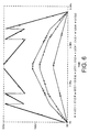
- Figs. 4-6 show examples of voltage traces produced as a result of switching from series to parallel connection of the capacitors CA1, CA2, CB1, and CB2.
- the voltage V developed across the output capacitor CM is measured, the capacitor CM being charged and discharged within the range of the rated voltage of the load.
- the state of charge is detected, based on the voltage V.
- the residual amount of energy can also be found from the voltage V.
- An example of a control circuit having a function of displaying or indicating the residual amount of energy is shown in Fig. 3.
- a voltage detection circuit 11 measures the voltage V developed across the output main capacitor CM.
- a voltage-judging circuit 12 judges the voltage from the voltage V, i.e., judges the state of charge.
- a switch control circuit 13 turns on and off the switches according to the result of the decision made by the voltage-judging circuit 12.
- a residual amount-calculation circuit 14 calculates the amount of residual energy from the voltage V.
- a display circuit 15 displays the amount of residual energy calculated by the residual amount-calculation circuit 14.
- Fig. 2(B) The circuit of Fig. 2(B) for switching the connection of the capacitors CA1, CA2, CB1, and CB2 between series and parallel connection is modeled, and all the capacitors are assumed to have the same capacitance.
- the resulting voltage trace is shown in Fig. 4.
- a heavy voltage burden is imposed on the capacitors CA1 and CB1. Therefore, capacitors CA1, CB1 and capacitors CA2, CB2 that are different in capacitance are used.
- the terminal voltage of the capacitor CM holds a certain relation to the amount of residual storage energy in the system.
- the terminal voltage of the capacitor CM is measured, and the terminal voltage V can be converted into the amount of residual storage energy, i.e., the amount of electrical storage energy, using this relation.
- the amount of the residual energy can be displayed by displaying the result of the conversion.
- the conversion based on the formula described above can be carried out in practice, using an arithmetic means or a circuit approximating a bent line of squares or root mean square.
- connection of plural capacitors of the power supply system are switched in a stepwise fashion according to the state of charge as described above to suppress variations in the voltage within a desired range
- variations in the voltage can be reduced further with small capacitances and high efficiency by adding simple voltage-compensating circuits. Examples of the structure are given below.
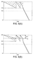
- Figs. 7A and 7B show diagrams of a further power supply system comprising capacitors connected switchably in accordance with the invention.
- Figs. 8A and 8B show diagrams depicting examples of transition of voltage allotment in a voltage-compensating circuit.
- Fig. 9 is a diagram showing an example using a capacitor-assisting power supply.
- Fig. 10 shows an example of the waveform illustrating the operation where the capacitor-assisting power supply is employed.
- a power supply 21 comprising capacitors, voltage-compensating circuits 22, 22-1, 22-2, voltage detection circuits 23, 24, a target value-calculating circuit 25, an error-detecting circuit 26, a voltage-compensating control circuit 27, a voltage-compensating capacitor Cc, an output capacitor Co, diodes Dc, Do, a choke coil L, a switching device Sw, and switches S11, S12, S21, S22.
- the power supply 21 comprising capacitors switches the connection of plural capacitors in a stepwise fashion and adjusts the output voltage.
- this power supply 21 is the power supply already described in connection with Figs. 1 and 2.
- the power supply 21 may be the power supply shown in Fig. 11.
- the power supply 21 may be a power supply in which voltage-adjusting capacitors are selectively connected in series with a main capacitor in a stepwise fashion or disconnected from the main capacitor in response to variations in the voltage across the main capacitor.
- Each of the voltage-compensating circuits 22, 22-1, and 22-2 is a circuit for compensating for variations in the voltage across the power supply 21, and compensates for the voltage in response to decrease in the voltage from the power supply 21.
- the voltage detection circuit 23 acts to detect the voltage across the power supply 21 comprising capacitors.
- the target value-calculating circuit 25 calculates a target value from the voltage across the capacitor power supply 21.
- the voltage detection circuit 24 serves to detect the voltage across the voltage-compensating circuit.
- the error-detecting circuit 26 compares a voltage detected by the voltage detection circuit 24 with a target value calculated by the target value-calculating circuit 25 and produces an error signal corresponding to the difference.
- the voltage-compensating circuit 27 controls the voltage-compensating circuit according to the error signal such that the voltage across the voltage-compensating circuit becomes equal to the target value.
- the target value-calculating circuit 25 calculates the target value for the voltage-compensating circuit from the voltage delivered from the capacitor power supply 21.
- the error-detecting circuit 26 produces the error signal according to the found target value.
- the voltage-compensating control circuit 27 controls the voltage-compensating circuit 22-2 so that the detected error signal is reduced down to zero. In this way, variations in the voltage across the capacitor power supply 21 are suppressed to some extent. For example, where variations in the voltage across the capacitor power supply 21 should be fully compensated for by the voltage-compensating circuit, the target value-calculating circuit 25 subtracts the voltage across the capacitor power supply 21 from a constant value to obtain a target value.
- the compensated voltage is kept at 200 V by the compensation made by the voltage-compensating circuit.
- the voltage-compensating circuit makes compensation as indicated by the hatching in Fig. 8(a). In consequence, a voltage-compensating capacity up to 60 V is required.
- the target value can be halved by the target value-calculating circuit 25. Voltage variations as indicated by the solid line are tolerated. In this case, the voltage-compensating circuit may make voltage compensation corresponding to the hatching. The amount of compensation is half the amount of compensation in the case of complete compensation shown in Fig. 8(a).
- a circuit using step-up type switching converters as the voltage-compensating circuits 22-1 and 22-2 are shown in Figs. 7(A)-(C).
- the duty cycle of a switching element Sw is controlled according to the error, or difference, between the detected value and a target value, thus controlling the voltage across a voltage-compensating capacitor Cc.
- the capacity of the converter is only 10% of the capacity where the whole output capacity is controlled by an output converter and taken.
- a bank producing an output voltage that varies by about 35% would not normally be used in AC-DC converters for power applications or in large-sized motor drivers of more than 100 kV. If variations are suppressed within about 10%, the circuit can be operated in these applications without trouble.
- the target value calculated by the target value-calculating circuit 25 is set to 25%, and compensation can be made by the voltage-compensating circuit 22.
- the voltage-compensating circuit uses a switching converter as mentioned above.
- the voltage-compensating capacitor Cc may be connected switchably via selector switches S11, S12, S21, and S22 as shown in Fig. 9.
- the polarity of the connected terminal of the voltage-compensating capacitor Cc is switched using a circuit for closing the selector switches S11, S21, a circuit for opening S12, S22, a circuit for opening the selector switches S11, S21, and a circuit for closing S12, S22.
- Variation of the output voltage V(9) can be nearly halved as shown in Fig. 10.
- control and rectification means are circuits using thyristors (unidirectional control and rectification devices) or triacs (bidirectional control and rectification devices).
- the control and rectification means may contain giant transistors, MOSFETs, other semiconductor control devices, or non-semiconductor control devices. Combinations of them may also be used.
- detection of the state of charge for controlling a switching circuit is carried out using the voltage across the main capacitor. Instead, the voltage across other capacitor may be employed.
- calculations are performed according to the voltage across a capacitor power supply to set a target value for a voltage-compensating circuit.
- a table holding data indicating the relation between a voltage and a target value may be established.
- the target value may be set by other calculation.
Abstract
Description
Claims (12)
- A power supply system having capacitors switchably connected to produce an adjustable output voltage, said power supply system comprising:a first set of capacitors connected in series at their series junctions;a second set of capacitors connected in series at their series junctions, the capacitors of said second set being equal in number with the capacitors of said first set;a series connection means connected with first terminals of the capacitors of said first and second sets to connect said first set of capacitors in series with said second set of capacitors;input/output terminals connected with second terminals of the capacitors of said first and second sets, said second terminals being not connected with said series connection means;a first series junction at which said first set of capacitors is connected with said series connection means;a first set of switching means for connecting said first series junction with said second terminals of said capacitors of said second set and with the series junctions of the capacitors of said second set;a second series junction at which said second set of capacitors is connected with said series connection means;a second set of switching means for connecting said second series junction with said second terminals of the capacitors of said first set and with the series junctions of the capacitors of said first set; anda control means for controlling said first set of switching means, said second set of switching means, and said series connection means to switch connection of said capacitors of the first and second sets among a first state in which said first set of capacitors is connected in series with said second set of capacitors, a second state in which said first set of capacitors is connected in parallel with said second set of capacitors, and a third state in which one or more capacitors of said first set are connected in parallel with one or more capacitors of said second set.
- The power supply system of claim 1, wherein said control means selectively turns on any one pair of switches of said first and second sets symmetrical with respect to said series connection means and said series connection switching means.
- The power supply system of claim 2, wherein said control means switches said switching means in such a way that whenever a terminal voltage developed across said input/output terminals reaches a given value by charging, said terminal voltage drops by a given small amount.
- The power supply system of claim 3, wherein said control means turns on said series connection switching means when charging is started.
- The power supply system of claim 2, wherein said control means switches said switching means in such a way that whenever a terminal voltage developed across said input/output terminals reaches a given value by discharging, said terminal voltage increases by a given small amount.
- The power supply system of claim 5, wherein said control means controls said switching means to connect said first and second sets of capacitors in parallel with each other when discharging is started.
- The power supply system of any one of claims 1-6, wherein said series connection switching means and said switching means are rectifier elements and control rectifier elements connected anti-parallel.
- A power supply system having capacitors switchably connected to produce an adjustable output voltage, said power supply system comprising:a first set of capacitors connected in series at their series junctions;a second set of capacitors connected in series at their series junctions, the capacitors of said second set being equal in number with the capacitors of said first set;a series connection means connected with first terminals of the capacitors of said first and second sets to connect said first set of capacitors in series with said second set of capacitors;input/output terminals connected with second terminals of the capacitors of said first and second sets, said second terminals being not connected with said series connection means;a first series junction at which said first set of capacitors is connected with said series connection means;a first set of switching means for connecting said first series junction with said second terminals of said capacitors of said second set and with the series junctions of the capacitors of said second set;a second series junction at which said second set of capacitors is connected with said series connection means;a second set of switching means for connecting said second series junction with said second terminals of said capacitors of said first set and with the series junctions of the capacitors of said first set;a control means for controlling said first set of switching means, said second set of switching means, and said series connection means to switch connection of said capacitors of the first and second sets among a first state in which said first set of capacitors is connected in series with said second set of capacitors, a second state in which said first set of capacitors is connected in parallel with said second set of capacitors, and a third state in which one or more capacitors of said first set are connected in parallel with one or more capacitors of said second set, said control means acting to control connection of the capacitors of said first and second sets between series connection and parallel connection, thus adjusting said output voltage; anda main capacitor bank with which said input/output terminals are connected in series.
- The power supply system of claim 8, wherein said series connection switching means and said switching means are rectifier elements and control rectifier means connected anti-parallel.
- A power supply system having capacitors switchably connected to produce an adjustable output voltage, said power supply system comprising:a capacitor power supply for switching connection of said capacitors in a stepwise fashion according to state of charge;a voltage-compensating circuit connected in series with said capacitor power supply and acting to make voltage compensation; anda control circuit for controlling a compensation voltage according to a voltage developed across said capacitor power supply, said voltage compensation circuit making voltage compensation at said compensation voltage.
- The power supply system of claim 10, wherein said voltage compensation circuit is a switching converter.
- The power supply system of claim 10, wherein said voltage compensation circuit is a circuit for inverting polarity and connecting capacitors.
Applications Claiming Priority (2)
| Application Number | Priority Date | Filing Date | Title |
|---|---|---|---|
| JP05241199A JP3487780B2 (en) | 1999-03-01 | 1999-03-01 | Connection switching control capacitor power supply |
| JP5241199 | 1999-03-01 |
Publications (2)
| Publication Number | Publication Date |
|---|---|
| EP1035637A2 true EP1035637A2 (en) | 2000-09-13 |
| EP1035637A3 EP1035637A3 (en) | 2002-02-20 |
Family
ID=12914055
Family Applications (1)
| Application Number | Title | Priority Date | Filing Date |
|---|---|---|---|
| EP00301666A Withdrawn EP1035637A3 (en) | 1999-03-01 | 2000-03-01 | Power supply system comprising capacitors connected switchably |
Country Status (3)
| Country | Link |
|---|---|
| US (1) | US6317343B1 (en) |
| EP (1) | EP1035637A3 (en) |
| JP (1) | JP3487780B2 (en) |
Cited By (13)
| Publication number | Priority date | Publication date | Assignee | Title |
|---|---|---|---|---|
| EP1300933A2 (en) * | 2001-10-02 | 2003-04-09 | Jeol Ltd. | Connection-switched capacitor storage system |
| WO2003067930A1 (en) * | 2002-02-04 | 2003-08-14 | Ricoh Company, Ltd. | Heating apparatus, fixing apparatus, and image forming apparatus |
| GB2444093A (en) * | 2006-11-22 | 2008-05-28 | Measurement Specialities Europ | Providing power from a piezoelectric source |
| DE102007060329A1 (en) * | 2007-12-14 | 2009-07-02 | Forschungszentrum Karlsruhe Gmbh | Capacitor block of interconnectable capacitors and method for loading and unloading the same |
| WO2010079258A1 (en) * | 2009-01-12 | 2010-07-15 | Kone Corporation | Transportation system |
| WO2010142373A3 (en) * | 2009-06-09 | 2011-10-13 | Audi Ag | On-board electrical system for a motor vehicle and method for operating an electrical load |
| EP2452426A1 (en) * | 2009-07-07 | 2012-05-16 | Auckland UniServices Limited | Transformer and priming circuit therefor |
| EP2469693A1 (en) * | 2010-12-23 | 2012-06-27 | Nxp B.V. | Power management device and method for harvesting discontinuous power source |
| US8629573B2 (en) | 2010-05-25 | 2014-01-14 | Audi Ag | On-board electrical system for a motor vehicle, motor vehicle and method for operating an on-board electrical system |
| CN104334393A (en) * | 2012-03-28 | 2015-02-04 | 罗伯特·博世有限公司 | Battery system, motor vehicle having a battery system, and method for starting up a battery system |
| CN107851521A (en) * | 2015-07-23 | 2018-03-27 | 布鲁解决方案公司 | The electric power system and electric vehicle of re-configurable capacitive energy storage device, integrated described device |
| WO2020064091A1 (en) * | 2018-09-25 | 2020-04-02 | Siemens Aktiengesellschaft | Switchable longitudinal voltage source, dc transmission system with longitudinal voltage source, and method for operating a longitudinal voltage source |
| WO2021165650A1 (en) * | 2020-02-21 | 2021-08-26 | Dyson Technology Limited | Reconfigurable battery pack |
Families Citing this family (30)
| Publication number | Priority date | Publication date | Assignee | Title |
|---|---|---|---|---|
| JP2002034179A (en) * | 2000-07-14 | 2002-01-31 | Toshiba Corp | Power controller |
| US6793793B2 (en) | 2000-08-24 | 2004-09-21 | Hideo Yoshida | Electrochemical treating method such as electroplating and electrochemical reaction device therefor |
| US6563235B1 (en) * | 2000-10-03 | 2003-05-13 | National Semiconductor Corporation | Switched capacitor array circuit for use in DC-DC converter and method |
| JP2002315308A (en) * | 2001-04-10 | 2002-10-25 | Fujitsu Ltd | Dc-dc converter and memory thereof |
| US6791210B2 (en) * | 2002-06-20 | 2004-09-14 | Intel Corporation | Cyclic regulation apparatus, system, and method |
| US6798162B2 (en) | 2002-07-17 | 2004-09-28 | Siemens Vdo Automotive Inc. | 12/42 volt DC brush motor control system |
| JP3781124B2 (en) * | 2004-03-29 | 2006-05-31 | 東光電気株式会社 | Capacitor power storage device |
| EP1641099A1 (en) * | 2004-09-24 | 2006-03-29 | Conception et Développement Michelin S.A. | Detachable charge control circuit for balancing the voltage of supercapacitors connected in series |
| US7109686B2 (en) * | 2004-11-15 | 2006-09-19 | Ise Corporation | System and method for precharging and discharging a high power ultracapacitor pack |
| JP5566568B2 (en) * | 2007-03-27 | 2014-08-06 | ピーエスフォー ルクスコ エスエイアールエル | Power supply voltage generation circuit |
| WO2009155986A1 (en) * | 2008-06-27 | 2009-12-30 | Abb Research Ltd | Battery energy source arrangement and voltage source converter system |
| DE102009034596A1 (en) * | 2009-07-24 | 2011-02-03 | Continental Automotive Gmbh | Electrical energy storing system for e.g. electric vehicle, has switching device connecting compensation cell to storage arrangement, so that difference of potential between storage arrangement and another storage arrangement is minimized |
| JP2011239603A (en) * | 2010-05-12 | 2011-11-24 | Tamura Seisakusho Co Ltd | Charge and discharge system |
| US20120025614A1 (en) * | 2010-07-28 | 2012-02-02 | Pasi Taimela | Uninterruptible Power Supply Apparatus and Methods Using Reconfigurable Energy Storage Networks |
| DE102010041029A1 (en) | 2010-09-20 | 2012-03-22 | Sb Limotive Company Ltd. | Method for starting up a battery system with a DC intermediate circuit |
| CA3025336A1 (en) | 2010-09-30 | 2012-03-30 | Philips Lighting Holding B.V. | Apparatus and methods for supplying power |
| US8633669B2 (en) | 2010-12-24 | 2014-01-21 | Marc Henness | Electrical circuit for controlling electrical power to drive an inductive load |
| EP2498368B1 (en) * | 2011-03-09 | 2014-08-06 | NIM Energy | Electrical energy buffering system |
| DE102012001390A1 (en) * | 2012-01-26 | 2013-08-01 | Sew-Eurodrive Gmbh & Co. Kg | Energy storage unit e.g. battery, has subsets whose terminals are fed in connecting elements that comprise electrical interconnections, where interconnections are connectable such that voltage or capacitance are adjustable from terminals |
| US9553517B2 (en) | 2013-03-01 | 2017-01-24 | Fllexgen Power Systems, Inc. | Hybrid energy storage system and methods |
| JP6368771B2 (en) | 2013-04-11 | 2018-08-01 | ライオン セミコンダクター インク. | Apparatus, system, and method for providing a hybrid voltage regulator |
| ES2819248T3 (en) | 2014-12-30 | 2021-04-15 | Flexgen Power Systems Inc | Transient power stabilization device with active and reactive power control |
| JP6183395B2 (en) * | 2015-03-26 | 2017-08-23 | 日本電気株式会社 | Power supply control system and power supply control method |
| US10205313B2 (en) | 2015-07-24 | 2019-02-12 | Symptote Technologies, LLC | Two-transistor devices for protecting circuits from sustained overcurrent |
| KR102521293B1 (en) | 2015-09-21 | 2023-04-12 | 심프토트 테크놀로지스 엘엘씨 | The single transistor apparatus for the circuit protection and autocatalytic voltage change |
| JP6631174B2 (en) * | 2015-11-06 | 2020-01-15 | 株式会社Ihi | Charge control device |
| US11043979B2 (en) * | 2017-08-08 | 2021-06-22 | Sony Semiconductor Solutions Corporation | Transmission device and communication system |
| KR101997844B1 (en) * | 2017-11-08 | 2019-07-08 | 충북대학교 산학협력단 | Step-wise split capacitor charging with high energy efficiency |
| US10601311B2 (en) | 2018-02-13 | 2020-03-24 | Lion Semiconductor Inc. | Circuits and methods for hybrid 3:1 voltage regulators |
| GB2592247B (en) * | 2020-02-21 | 2023-09-20 | Dyson Technology Ltd | Reconfigurable battery pack |
Citations (3)
| Publication number | Priority date | Publication date | Assignee | Title |
|---|---|---|---|---|
| US3497792A (en) | 1967-11-20 | 1970-02-24 | Westinghouse Electric Corp | High voltage to low voltage inverters |
| US5414614A (en) | 1994-06-06 | 1995-05-09 | Motorola, Inc. | Dynamically configurable switched capacitor power supply and method |
| JPH0947018A (en) | 1995-07-25 | 1997-02-14 | Sony Corp | Dc-dc converter |
Family Cites Families (9)
| Publication number | Priority date | Publication date | Assignee | Title |
|---|---|---|---|---|
| JPS60131074A (en) * | 1983-12-16 | 1985-07-12 | Toshiba Corp | Multiple voltage rectifier circuit |
| US5364801A (en) * | 1990-12-17 | 1994-11-15 | Texas Instruments Incorporated | Method of forming a charge pump circuit |
| DE69205885T2 (en) * | 1991-05-15 | 1996-06-13 | Matsushita Electric Works Ltd | Apparatus for operating discharge lamps. |
| JP2596314B2 (en) * | 1993-05-31 | 1997-04-02 | 日本電気株式会社 | Switching power supply circuit |
| JPH07231648A (en) * | 1994-02-15 | 1995-08-29 | Matsushita Electric Works Ltd | Power supply unit |
| US5734205A (en) * | 1996-04-04 | 1998-03-31 | Jeol Ltd. | Power supply using batteries undergoing great voltage variations |
| JP3224744B2 (en) * | 1996-07-08 | 2001-11-05 | 富士通株式会社 | Step-down DC-DC regulator |
| US5886887A (en) * | 1997-03-27 | 1999-03-23 | Integrated Memory Technologies, Inc. | Voltage multiplier with low threshold voltage sensitivity |
| EP0899946A3 (en) * | 1997-08-26 | 2001-08-16 | Eastman Kodak Company | Image sensor electronics |
-
1999
- 1999-03-01 JP JP05241199A patent/JP3487780B2/en not_active Expired - Fee Related
-
2000
- 2000-03-01 EP EP00301666A patent/EP1035637A3/en not_active Withdrawn
- 2000-03-01 US US09/516,570 patent/US6317343B1/en not_active Expired - Lifetime
Patent Citations (3)
| Publication number | Priority date | Publication date | Assignee | Title |
|---|---|---|---|---|
| US3497792A (en) | 1967-11-20 | 1970-02-24 | Westinghouse Electric Corp | High voltage to low voltage inverters |
| US5414614A (en) | 1994-06-06 | 1995-05-09 | Motorola, Inc. | Dynamically configurable switched capacitor power supply and method |
| JPH0947018A (en) | 1995-07-25 | 1997-02-14 | Sony Corp | Dc-dc converter |
Cited By (27)
| Publication number | Priority date | Publication date | Assignee | Title |
|---|---|---|---|---|
| EP1300933A2 (en) * | 2001-10-02 | 2003-04-09 | Jeol Ltd. | Connection-switched capacitor storage system |
| EP1300933A3 (en) * | 2001-10-02 | 2005-06-01 | Advanced Capacitor Technologies, Inc. | Connection-switched capacitor storage system |
| WO2003067930A1 (en) * | 2002-02-04 | 2003-08-14 | Ricoh Company, Ltd. | Heating apparatus, fixing apparatus, and image forming apparatus |
| US7002112B2 (en) | 2002-02-04 | 2006-02-21 | Ricoh Company, Ltd. | Heating apparatus for increasing temperature in short period of time with minimum overshoot |
| US7247816B2 (en) | 2002-02-04 | 2007-07-24 | Ricoh Company, Ltd. | Heating apparatus, fixing apparatus, and image forming apparatus |
| US7546050B2 (en) | 2002-02-04 | 2009-06-09 | Ricoh Company, Ltd. | Fixing apparatus including a fixing roller and a pressurization roller |
| GB2444093A (en) * | 2006-11-22 | 2008-05-28 | Measurement Specialities Europ | Providing power from a piezoelectric source |
| GB2444093B (en) * | 2006-11-22 | 2009-05-20 | Measurement Specialities Europ | Method and apparatus for providing power to an electronic system |
| DE102007060329A1 (en) * | 2007-12-14 | 2009-07-02 | Forschungszentrum Karlsruhe Gmbh | Capacitor block of interconnectable capacitors and method for loading and unloading the same |
| US8177033B2 (en) | 2009-01-12 | 2012-05-15 | Kone Corporation | Transportation system with capacitive energy storage and non-volatile memory for storing the operational state of the transportation system upon detection of the operational anomaly in power |
| CN102272032B (en) * | 2009-01-12 | 2014-10-22 | 通力股份公司 | Transportation system |
| CN102272032A (en) * | 2009-01-12 | 2011-12-07 | 通力股份公司 | Transportation system |
| WO2010079258A1 (en) * | 2009-01-12 | 2010-07-15 | Kone Corporation | Transportation system |
| WO2010142373A3 (en) * | 2009-06-09 | 2011-10-13 | Audi Ag | On-board electrical system for a motor vehicle and method for operating an electrical load |
| US9024466B2 (en) | 2009-06-09 | 2015-05-05 | Audi Ag | On-board electrical system for a motor vehicle and method for operating an electrical load |
| US10250166B2 (en) | 2009-07-07 | 2019-04-02 | Auckland Uniservices Limited | Transformer and priming circuit therefor |
| EP2452426A4 (en) * | 2009-07-07 | 2013-10-30 | Auckland Uniservices Ltd | Transformer and priming circuit therefor |
| EP2452426A1 (en) * | 2009-07-07 | 2012-05-16 | Auckland UniServices Limited | Transformer and priming circuit therefor |
| US8629573B2 (en) | 2010-05-25 | 2014-01-14 | Audi Ag | On-board electrical system for a motor vehicle, motor vehicle and method for operating an on-board electrical system |
| US8854847B2 (en) | 2010-12-23 | 2014-10-07 | Nxp, B.V. | Power and management device and method |
| EP2469693A1 (en) * | 2010-12-23 | 2012-06-27 | Nxp B.V. | Power management device and method for harvesting discontinuous power source |
| CN104334393A (en) * | 2012-03-28 | 2015-02-04 | 罗伯特·博世有限公司 | Battery system, motor vehicle having a battery system, and method for starting up a battery system |
| CN107851521A (en) * | 2015-07-23 | 2018-03-27 | 布鲁解决方案公司 | The electric power system and electric vehicle of re-configurable capacitive energy storage device, integrated described device |
| WO2020064091A1 (en) * | 2018-09-25 | 2020-04-02 | Siemens Aktiengesellschaft | Switchable longitudinal voltage source, dc transmission system with longitudinal voltage source, and method for operating a longitudinal voltage source |
| US11411511B2 (en) | 2018-09-25 | 2022-08-09 | Siemens Energy Global GmbH & Co. KG | Switchable longitudinal voltage source, direct current transmission system with longitudinal voltage source and method for operating a longitudinal voltage source |
| WO2021165650A1 (en) * | 2020-02-21 | 2021-08-26 | Dyson Technology Limited | Reconfigurable battery pack |
| GB2592248B (en) * | 2020-02-21 | 2023-10-11 | Dyson Technology Ltd | Reconfigurable battery pack |
Also Published As
| Publication number | Publication date |
|---|---|
| JP2000253572A (en) | 2000-09-14 |
| JP3487780B2 (en) | 2004-01-19 |
| US6317343B1 (en) | 2001-11-13 |
| EP1035637A3 (en) | 2002-02-20 |
Similar Documents
| Publication | Publication Date | Title |
|---|---|---|
| EP1035637A2 (en) | Power supply system comprising capacitors connected switchably | |
| KR102120797B1 (en) | Battery charging-discharging apparatus and method | |
| US11581811B2 (en) | Multi-phase parallel converter and controlling method therefor | |
| US20170271864A1 (en) | System and method for connecting a first battery in parallel with a second battery by discharging for equalization | |
| US7394673B2 (en) | Switching power supply apparatus provided with series-connected charge pump circuits | |
| JP4079403B2 (en) | Series-parallel switching capacitor power storage device | |
| US20140306673A1 (en) | Apparatus, systems, and methods for providing a hybrid power regulator | |
| EP1716625A2 (en) | More compact and higher reliability power supply module | |
| CN114142723B (en) | Power conversion structure and electronic equipment comprising same | |
| CN114498866B (en) | Dual-battery charging device and method and controller thereof | |
| US7759905B2 (en) | Linear battery charger | |
| Dahono et al. | A family of modular multilevel bidirectional DC-DC converters for high voltage-ratio and low-ripple applications | |
| JPH08205524A (en) | Voltage converter | |
| CN114487900A (en) | Short-circuit detection device and control method of switched capacitor converter | |
| JP3418951B2 (en) | Series / parallel switching power supply | |
| JP3529623B2 (en) | Apparatus and method for detecting remaining capacity of series-parallel switching storage power supply | |
| JP3594288B2 (en) | Capacitor power supply with switchable number of series connection stages | |
| JP3414655B2 (en) | Series switching capacitor power supply | |
| JP3311670B2 (en) | Series / parallel switching power supply | |
| Khan et al. | An Auxiliary-Assisted Dual-Inductor Hybrid DC-DC Converter with Adaptive Inductor Slew Rate for Fast Transient Response in 48-V Automotive PoL Applications | |
| JP3351741B2 (en) | Power supply unit with connection bank number control | |
| Bansal et al. | Characterization and Steady State Analysis of Multiport Switched Boost Converter | |
| Ramos-Ruiz et al. | Medium voltage AC-AC adapter using multilevel capacitor clamped buck converter | |
| CN117353578B (en) | Three-level Buck direct current converter and control method | |
| US20230353054A1 (en) | Multi-stage dc-dc converter |
Legal Events
| Date | Code | Title | Description |
|---|---|---|---|
| PUAI | Public reference made under article 153(3) epc to a published international application that has entered the european phase |
Free format text: ORIGINAL CODE: 0009012 |
|
| AK | Designated contracting states |
Kind code of ref document: A2 Designated state(s): AT BE CH CY DE DK ES FI FR GB GR IE IT LI LU MC NL PT SE Kind code of ref document: A2 Designated state(s): DE FR GB IT SE |
|
| AX | Request for extension of the european patent |
Free format text: AL;LT;LV;MK;RO;SI |
|
| PUAL | Search report despatched |
Free format text: ORIGINAL CODE: 0009013 |
|
| RIC1 | Information provided on ipc code assigned before grant |
Free format text: 7H 02M 3/07 A, 7H 02M 1/14 B |
|
| AK | Designated contracting states |
Kind code of ref document: A3 Designated state(s): AT BE CH CY DE DK ES FI FR GB GR IE IT LI LU MC NL PT SE |
|
| AX | Request for extension of the european patent |
Free format text: AL;LT;LV;MK;RO;SI |
|
| 17P | Request for examination filed |
Effective date: 20020529 |
|
| AKX | Designation fees paid |
Free format text: DE FR GB IT SE |
|
| RAP1 | Party data changed (applicant data changed or rights of an application transferred) |
Owner name: OKAMURA LABORATORY INC. Owner name: ADVANCED CAPACITOR TECHNOLOGIES, INC. Owner name: KABUSHIKI KAISHA POWERSYSTEMS |
|
| 17Q | First examination report despatched |
Effective date: 20081028 |
|
| GRAP | Despatch of communication of intention to grant a patent |
Free format text: ORIGINAL CODE: EPIDOSNIGR1 |
|
| STAA | Information on the status of an ep patent application or granted ep patent |
Free format text: STATUS: THE APPLICATION IS DEEMED TO BE WITHDRAWN |
|
| 18D | Application deemed to be withdrawn |
Effective date: 20110823 |