EP1034932A2 - Printhead having varied thickness passivation layer and method of making same - Google Patents
Printhead having varied thickness passivation layer and method of making same Download PDFInfo
- Publication number
- EP1034932A2 EP1034932A2 EP00301608A EP00301608A EP1034932A2 EP 1034932 A2 EP1034932 A2 EP 1034932A2 EP 00301608 A EP00301608 A EP 00301608A EP 00301608 A EP00301608 A EP 00301608A EP 1034932 A2 EP1034932 A2 EP 1034932A2
- Authority
- EP
- European Patent Office
- Prior art keywords
- passivation layer
- thickness
- over
- substrate
- expulsion element
- Prior art date
- Legal status (The legal status is an assumption and is not a legal conclusion. Google has not performed a legal analysis and makes no representation as to the accuracy of the status listed.)
- Granted
Links
Images
Classifications
-
- B—PERFORMING OPERATIONS; TRANSPORTING
- B41—PRINTING; LINING MACHINES; TYPEWRITERS; STAMPS
- B41J—TYPEWRITERS; SELECTIVE PRINTING MECHANISMS, i.e. MECHANISMS PRINTING OTHERWISE THAN FROM A FORME; CORRECTION OF TYPOGRAPHICAL ERRORS
- B41J2/00—Typewriters or selective printing mechanisms characterised by the printing or marking process for which they are designed
- B41J2/005—Typewriters or selective printing mechanisms characterised by the printing or marking process for which they are designed characterised by bringing liquid or particles selectively into contact with a printing material
- B41J2/01—Ink jet
- B41J2/135—Nozzles
- B41J2/16—Production of nozzles
- B41J2/1621—Manufacturing processes
- B41J2/1631—Manufacturing processes photolithography
-
- B—PERFORMING OPERATIONS; TRANSPORTING
- B41—PRINTING; LINING MACHINES; TYPEWRITERS; STAMPS
- B41J—TYPEWRITERS; SELECTIVE PRINTING MECHANISMS, i.e. MECHANISMS PRINTING OTHERWISE THAN FROM A FORME; CORRECTION OF TYPOGRAPHICAL ERRORS
- B41J2/00—Typewriters or selective printing mechanisms characterised by the printing or marking process for which they are designed
- B41J2/005—Typewriters or selective printing mechanisms characterised by the printing or marking process for which they are designed characterised by bringing liquid or particles selectively into contact with a printing material
- B41J2/01—Ink jet
- B41J2/135—Nozzles
- B41J2/14—Structure thereof only for on-demand ink jet heads
- B41J2/14016—Structure of bubble jet print heads
- B41J2/14088—Structure of heating means
- B41J2/14112—Resistive element
- B41J2/14129—Layer structure
-
- B—PERFORMING OPERATIONS; TRANSPORTING
- B41—PRINTING; LINING MACHINES; TYPEWRITERS; STAMPS
- B41J—TYPEWRITERS; SELECTIVE PRINTING MECHANISMS, i.e. MECHANISMS PRINTING OTHERWISE THAN FROM A FORME; CORRECTION OF TYPOGRAPHICAL ERRORS
- B41J2/00—Typewriters or selective printing mechanisms characterised by the printing or marking process for which they are designed
- B41J2/005—Typewriters or selective printing mechanisms characterised by the printing or marking process for which they are designed characterised by bringing liquid or particles selectively into contact with a printing material
- B41J2/01—Ink jet
- B41J2/135—Nozzles
- B41J2/16—Production of nozzles
- B41J2/1601—Production of bubble jet print heads
- B41J2/1603—Production of bubble jet print heads of the front shooter type
-
- B—PERFORMING OPERATIONS; TRANSPORTING
- B41—PRINTING; LINING MACHINES; TYPEWRITERS; STAMPS
- B41J—TYPEWRITERS; SELECTIVE PRINTING MECHANISMS, i.e. MECHANISMS PRINTING OTHERWISE THAN FROM A FORME; CORRECTION OF TYPOGRAPHICAL ERRORS
- B41J2/00—Typewriters or selective printing mechanisms characterised by the printing or marking process for which they are designed
- B41J2/005—Typewriters or selective printing mechanisms characterised by the printing or marking process for which they are designed characterised by bringing liquid or particles selectively into contact with a printing material
- B41J2/01—Ink jet
- B41J2/135—Nozzles
- B41J2/16—Production of nozzles
- B41J2/1621—Manufacturing processes
- B41J2/1626—Manufacturing processes etching
- B41J2/1629—Manufacturing processes etching wet etching
-
- B—PERFORMING OPERATIONS; TRANSPORTING
- B41—PRINTING; LINING MACHINES; TYPEWRITERS; STAMPS
- B41J—TYPEWRITERS; SELECTIVE PRINTING MECHANISMS, i.e. MECHANISMS PRINTING OTHERWISE THAN FROM A FORME; CORRECTION OF TYPOGRAPHICAL ERRORS
- B41J2202/00—Embodiments of or processes related to ink-jet or thermal heads
- B41J2202/01—Embodiments of or processes related to ink-jet heads
- B41J2202/13—Heads having an integrated circuit
Definitions
- the present invention relates to the structure of printheads that are used in ink jet printers and the like and, more specifically, to varying the thickness of the passivation layer thereof to improve performance and protect circuit components.
- Ink jet printers are known in the art and include those made by Hewlett-Packard, Canon and Epson, among other producers. Ink jet printers function by several actuation mechanisms, including thermal (heating resistor) or mechanical (piezo-electric) actuators. While the discussion herein is primarily directed toward thermally actuated printheads, it should be recognized that the varied passivation layer thickness of the present invention are also applicable to mechanically actuated printheads. As discussed in more detail below, the present invention is concerned with providing a thick passivation layer to protect circuitry on a printhead die, while providing a thin passivation layer over the ink expulsion element to reduce ink expulsion energy. A thin passivation layer reduces the energy required to expel ink, regardless of the type of actuator and thus the present invention is applicable to all ink jet and related printers.
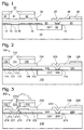
- Fig. 1 illustrates a representative printhead structure of a prior art ink jet printhead that is thermally actuated.
- the structure of Fig. 1 includes a substrate 10 usually of semiconductive material in which is formed a resistive layer and element 12.
- a layer of conductive material 14 (usually aluminum or the like) is formed on the substrate, generally as shown.
- a passivation layer 20 (normally Si 3 N 4 /SiC or the like) is formed on the substrate, and a metallic layer 26 and contact pad 28 (coupled through via 25) are formed on the passivation layer.
- the metallic or conductive layer may include a protection/cavitation layer 24 and a surface conductor 26.
- An inkwell 31, barrier layer 32 and orifice plate 33 are provided as is known.
- a printhead "fire" signal is propagated from circuit 50 or from an off-chip source to the resistive element and there produces sufficient heat to cause a drop of ink to be expelled through the orifice plate 33.
- TOE turn-on energy
- a thin passivation layer has disadvantageous aspects.
- One disadvantageous aspect is that as the passivation layer thickness is reduced, the likelihood of a passivation layer crack or other defect increases.
- steps such as beveling the transitions of the underlying topology, particularly those near the resistive element (which is a place of higher physical stress) have been undertaken.
- edges 13,15 of the conductive layer 14 proximate resistive element 12 may be beveled. While beveling reduces physical stresses on the passivation layer, it is significantly more difficult to precisely position a beveled edge than to position a straight (vertical) edge.
- the significant margins of error in beveled edge placement result in significant variability in the defined resistor size and amount of heat generated thereby. This in turn results in inconsistent firing of the printhead and inconsistent print intensity, among other problems.
- Another disadvantageous aspect of a thin passivation layer relates to the expanded use of the printhead die or substrate 10 for processing logic 50.
- the number of individual firing chambers in a printhead die increases, the number of power conductors and signal conductors for these firing chambers increases. These conductors are usually formed on top of the passivation layer.
- passivation layer thicknesses decrease and the provision of surface conductors increases, the likelihood of capacitive coupling or the like effecting circuitry within the substrate increases.
- increasing passivation layer thickness disadvantageously increases the TOE.
- the printhead 100 includes a substrate 110 on which is formed an ink expulsion (e.g., resistive) element 112, conductive layer 114, passivation layer 120, protection/cavitation layer 124, surface conductor 126 and contact pad 128.
- An inkwell 131, barrier layer 132 and orifice plate 133 are also provided in printhead 100.
- the substrate 110 in which the printhead is formed also includes control logic 150 that is coupled off die through contact pad 128 and to other locations as is known in the art. Control logic 150 may include digital and/or analog circuitry.
- Printhead 100 is formed such that the passivation layer 120 includes a region 121 over ink expulsion element 112 that is relatively thin and a region 122 over circuit 150 that is relatively thick.
- ink expulsion element 112 is a resistive element or other thermal actuation element, though it should be recognized that a mechanical actuation element may be utilized.
- Thinning the passivation layer from 0.75 microns to 0.38 microns achieves a TOE reduction of approximately 22%.
- the passivation layer in region 121 may be reduced below 0.38 microns, for example, to 0.2 microns or below.
- the lower limit of passivation layer thickness is determined at least in part by the minimum thickness before breakdown of the layer due to mechanical or electrical stresses and to deleterious impact on resistor life.
- region 122 of the passivation layer can be made as thick as desired, for example, sufficiently thick to protect underlying circuitry 150.
- the thickness of passivation layer region 122 is preferably 1.0 micron to 1.5 micron, and can be made thicker if desired. The thickness limitations are driven by process capability and manufacturability, dry-etch considerations, number of masks, etc. In general, it is preferred that region 122 be as thick as necessary for its intended purpose without being overly thick.
- the printhead of Fig. 2 is preferably not made with beveled edges on the conductive layer 114 (as discussed above with reference to Fig. 1, though beveled edges may be provided without departing from the present invention).
- the variable passivation layer thickness techniques of the present invention permit formation of a passivation layer over the conductive layer edges (or "steps") that is at least twice as thick as the conductive layer (and sufficiently inwardly formed from the edges in the horizontal direction as to provide enhanced breakdown protection). This thickness provides protection against cracking and the like. Furthermore, as the thickness of the conductive layer decreases, the requisite thickness of the passivation layer also decreases.
- Fig. 2 may be formed generally as follows. Starting from the substrate with the control logic and resistive element formed therein, conductive layer 114 (preferably with straight edges) is formed on this structure. A single passivation material, for example, Si 3 N 4 , is preferably formed over the conductive layer and resistive element and the remainder of the substrate. It should be recognized that while Si 3 N 4 is preferred, layer 121 could be formed of another known passivation layer material or a combination of materials. The thickness of the initial passivation layer is preferably approximately 1 micron or other desired thickness. This initial passivation layer is then etched over the resistive element to form the thin passivation layer of region 121.
- a single passivation material for example, Si 3 N 4
- layer 121 could be formed of another known passivation layer material or a combination of materials.
- the thickness of the initial passivation layer is preferably approximately 1 micron or other desired thickness. This initial passivation layer is then etched over the resistive element to form the thin passivation layer of region 121.
- the passivation layer may be etched to a thickness of 0.2 microns or another appropriate dimension determined by the designer and limited by processing tolerances. The clearing of via 125 will typically require a separate photolithographic/etch step.
- the etched passivation layer is then covered where appropriate with a material such as tantalum or the like. Tantalum provides a cavitation surface 124 under ink well 131 and is also a suitable conductor for surface conductor 126.
- the tantalum is preferably applied to an approximate thickness of 0.6 microns.
- Contact pads 128 are then formed on the tantalum layer and these contact pads are preferably formed of gold.
- FIG. 3 illustrates a printhead having substantially the same components as in Fig. 2.
- Components of the printhead of Fig. 3 that correspond to components of the printhead of Fig. 2 have the same reference numeral with the most significant digit replaced with a 2.
- Printhead 200 is preferably formed in a manner discussed above for printhead 100, however, during the passivation layer etch over the resistive element, a complete etch is preferably performed, thus exposing the resistive element.
- a thin passivation layer e.g., Si 3 N 4 and/or SIC or both
- the new layer of material forms passivation layer region 221.
- This etch and selected refill method is performed in such a manner as to provide sufficient spacing from edges 213, 215 such that adequate passivation layer protection (i.e., breakdown protection) is provided. Tantalum and gold are then applied as discussed above or other conventional photolithographic process steps may be carried out.
- the complete etch and refill method permits more accurate control of the thickness of region 221. It does, however, require additional mask operations.
- the thicker passivation layer of the present invention is beneficial in protecting the front side of the substrate during a TMAH etch and the like.
- TMAH etches and the like are preformed to remove portions of the substrate and thus create ink conduits.
Landscapes
- Engineering & Computer Science (AREA)
- Manufacturing & Machinery (AREA)
- Particle Formation And Scattering Control In Inkjet Printers (AREA)
Abstract
Description
Claims (10)
- A printing apparatus, comprising:a substrate (110,210);an ink expulsion element (112,212) formed on said substrate at a first region thereof;a passivation layer (120,220) formed over said ink expulsion element and said substrate; andan ink well (131,231) formed over said ink expulsion element;
wherein a thickness of said passivation layer over said ink expulsion element (121,221) is thinner than a thickness of said passivation layer over another region of said substrate. - The apparatus of claim 1, further comprising processing logic (150,250) formed in said substrate, said processing logic being formed in said other region of said substrate.
- The apparatus of claim 1, wherein said passivation layer (120,220) is formed of a dielectric material.
- The apparatus of claim 1, further comprising a conductive layer (114,214) provided adjacent said ink expulsion element for delivering an electrical signal to said ink expulsion element, wherein the thickness of said passivation layer (121,221) over said ink expulsion element is less than approximately four times the thickness of said conductive layer.
- The apparatus of claim 1, further comprising a conductive layer (114,214) provided adjacent said ink expulsion element for delivering an electrical signal to said ink expulsion element, wherein said conductive layer has a substantially vertical edge (113,115,213,215) proximate said ink expulsion element.
- A method of forming a printhead, comprising the steps of:providing a substrate (110,210);forming an ink expulsion element (112,212) on said substrate at a first region of said substrate;forming a passivation layer (120,220) over said ink expulsion layer and substrate; andforming an ink well (131,231) over said ink expulsion element;
wherein said passivation layer is formed such that the passivation layer has a first thickness (121,221) over said ink expulsion element and a second thickness (122,222) over another region of said substrate, said first thickness being less that said second thickness. - The method of claim 6, wherein said passivation layer forming step comprises the steps of:forming an initial passivation layer of a given thickness; andproducing a thin passivation layer (121,221) by removing a portion of said initial passivation layer over said ink expulsion element to create said first thickness over said ink expulsion element that is less than said second thickness.
- The method of claim 6, wherein said passivation layer forming step comprises the step offorming an initial passivation layer of a given thickness; andremoving said initial passivation layer over said ink expulsion element; andproducing a thin passivation layer by reforming a passivation layer (121,221) over said ink expulsion element that is not as thick as said initial passivation layer (122,222) to thereby form said first thickness over said ink expulsion element that is less than said second thickness.
- The method of claim 7 or 8, wherein said thin passivation layer (121,221) producing step includes the step of forming said passivation layer over said ink expulsion element to a thickness of approximately 0.7 microns or less.
- The method of claim 7 or 8, wherein said step of forming said passivation layer (122,222) over said other region of said substrate includes the step of forming said passivation layer over said other region to a thickness of approximately 0.6 microns or more.
Applications Claiming Priority (2)
| Application Number | Priority Date | Filing Date | Title |
|---|---|---|---|
| US267216 | 1999-03-12 | ||
| US09/267,216 US6331049B1 (en) | 1999-03-12 | 1999-03-12 | Printhead having varied thickness passivation layer and method of making same |
Publications (3)
| Publication Number | Publication Date |
|---|---|
| EP1034932A2 true EP1034932A2 (en) | 2000-09-13 |
| EP1034932A3 EP1034932A3 (en) | 2001-01-03 |
| EP1034932B1 EP1034932B1 (en) | 2005-12-21 |
Family
ID=23017818
Family Applications (1)
| Application Number | Title | Priority Date | Filing Date |
|---|---|---|---|
| EP00301608A Expired - Lifetime EP1034932B1 (en) | 1999-03-12 | 2000-02-29 | Printhead having varied thickness passivation layer |
Country Status (4)
| Country | Link |
|---|---|
| US (1) | US6331049B1 (en) |
| EP (1) | EP1034932B1 (en) |
| JP (1) | JP3326152B2 (en) |
| DE (1) | DE60024905T2 (en) |
Cited By (2)
| Publication number | Priority date | Publication date | Assignee | Title |
|---|---|---|---|---|
| EP1219426A3 (en) * | 2000-12-29 | 2003-03-19 | Eastman Kodak Company | Cmos/mems integrated ink jet print head and method of forming same |
| CN109414929A (en) * | 2016-09-19 | 2019-03-01 | 惠普发展公司,有限责任合伙企业 | The termination ring of metal layer with band gap |
Families Citing this family (10)
| Publication number | Priority date | Publication date | Assignee | Title |
|---|---|---|---|---|
| US6676246B1 (en) | 2002-11-20 | 2004-01-13 | Lexmark International, Inc. | Heater construction for minimum pulse time |
| US6786575B2 (en) * | 2002-12-17 | 2004-09-07 | Lexmark International, Inc. | Ink jet heater chip and method therefor |
| US7195343B2 (en) * | 2004-08-27 | 2007-03-27 | Lexmark International, Inc. | Low ejection energy micro-fluid ejection heads |
| US7178904B2 (en) * | 2004-11-11 | 2007-02-20 | Lexmark International, Inc. | Ultra-low energy micro-fluid ejection device |
| US7837886B2 (en) * | 2007-07-26 | 2010-11-23 | Hewlett-Packard Development Company, L.P. | Heating element |
| US7862156B2 (en) * | 2007-07-26 | 2011-01-04 | Hewlett-Packard Development Company, L.P. | Heating element |
| US8350661B2 (en) * | 2009-05-26 | 2013-01-08 | Ovonyx, Inc. | Breakdown layer via lateral diffusion |
| PL2910380T3 (en) * | 2010-07-23 | 2018-06-29 | Hewlett-Packard Development Company, L.P. | Thermal resistor fluid ejection assembly |
| US9498953B2 (en) | 2013-01-23 | 2016-11-22 | Hewlett-Packard Development Company, L.P. | Printhead die with multiple termination rings |
| WO2019147217A1 (en) | 2018-01-23 | 2019-08-01 | Hewlett-Packard Development Company, L.P. | Fluidic dies with beveled edges underneath electrical leads |
Family Cites Families (35)
| Publication number | Priority date | Publication date | Assignee | Title |
|---|---|---|---|---|
| US4354309A (en) | 1978-12-29 | 1982-10-19 | International Business Machines Corp. | Method of manufacturing a metal-insulator-semiconductor device utilizing a graded deposition of polycrystalline silicon |
| JPS5931943B2 (en) | 1979-04-02 | 1984-08-06 | キヤノン株式会社 | liquid jet recording method |
| US4616408A (en) | 1982-11-24 | 1986-10-14 | Hewlett-Packard Company | Inversely processed resistance heater |
| US4513298A (en) | 1983-05-25 | 1985-04-23 | Hewlett-Packard Company | Thermal ink jet printhead |
| US4535343A (en) | 1983-10-31 | 1985-08-13 | Hewlett-Packard Company | Thermal ink jet printhead with self-passivating elements |
| JPS60116451A (en) * | 1983-11-30 | 1985-06-22 | Canon Inc | Liquid jet recording head |
| US4792818A (en) * | 1987-06-12 | 1988-12-20 | International Business Machines Corporation | Thermal drop-on-demand ink jet print head |
| US4931813A (en) | 1987-09-21 | 1990-06-05 | Hewlett-Packard Company | Ink jet head incorporating a thick unpassivated TaAl resistor |
| US4872028A (en) | 1988-03-21 | 1989-10-03 | Hewlett-Packard Company | Thermal-ink-jet print system with drop detector for drive pulse optimization |
| US4990939A (en) * | 1988-09-01 | 1991-02-05 | Ricoh Company, Ltd. | Bubble jet printer head with improved operational speed |
| US4982199A (en) | 1988-12-16 | 1991-01-01 | Hewlett-Packard Company | Method and apparatus for gray scale printing with a thermal ink jet pen |
| ES2055865T3 (en) * | 1989-04-18 | 1994-09-01 | Canon Kk | SUBSTRATE FOR AN INK SPRAY PRINTER HEAD, INK SPRAY PRINTER HEAD CONSTITUTED BY THE USE OF SUCH INK SPRAY AND PRINTING APPARATUS PROVIDED WITH SUCH A SPRAY HEAD. |
| US4951063A (en) | 1989-05-22 | 1990-08-21 | Xerox Corporation | Heating elements for thermal ink jet devices |
| US5227812A (en) | 1990-02-26 | 1993-07-13 | Canon Kabushiki Kaisha | Liquid jet recording head with bump connector wiring |
| US5187500A (en) | 1990-09-05 | 1993-02-16 | Hewlett-Packard Company | Control of energy to thermal inkjet heating elements |
| US5083137A (en) | 1991-02-08 | 1992-01-21 | Hewlett-Packard Company | Energy control circuit for a thermal ink-jet printhead |
| US5168284A (en) | 1991-05-01 | 1992-12-01 | Hewlett-Packard Company | Printhead temperature controller that uses nonprinting pulses |
| US5194877A (en) | 1991-05-24 | 1993-03-16 | Hewlett-Packard Company | Process for manufacturing thermal ink jet printheads having metal substrates and printheads manufactured thereby |
| US5257042A (en) | 1991-07-09 | 1993-10-26 | Xerox Corporation | Thermal ink jet transducer protection |
| JP3379106B2 (en) | 1992-04-23 | 2003-02-17 | セイコーエプソン株式会社 | Liquid jet head |
| JP3408292B2 (en) | 1992-09-09 | 2003-05-19 | ヒューレット・パッカード・カンパニー | Print head |
| US5357081A (en) | 1993-01-21 | 1994-10-18 | Hewlett-Packard Company | Power supply for individual control of power delivered to integrated drive thermal inkjet printhead heater resistors |
| US6070969A (en) * | 1994-03-23 | 2000-06-06 | Hewlett-Packard Company | Thermal inkjet printhead having a preferred nucleation site |
| US5660739A (en) * | 1994-08-26 | 1997-08-26 | Canon Kabushiki Kaisha | Method of producing substrate for ink jet recording head, ink jet recording head and ink jet recording apparatus |
| JPH08197732A (en) * | 1995-01-24 | 1996-08-06 | Canon Inc | Recording head and recording apparatus using the recording head |
| EP0729834B1 (en) | 1995-03-03 | 2002-06-12 | Canon Kabushiki Kaisha | An ink-jet head, a substrate for an ink-jet head, and an ink-jet apparatus |
| US5636441A (en) | 1995-03-16 | 1997-06-10 | Hewlett-Packard Company | Method of forming a heating element for a printhead |
| US20020063753A1 (en) | 1995-06-28 | 2002-05-30 | Masahiko Kubota | Liquid ejecting printing head, production method thereof and production method for base body employed for liquid ejecting printing head |
| JP3513270B2 (en) | 1995-06-30 | 2004-03-31 | キヤノン株式会社 | Ink jet recording head and ink jet recording apparatus |
| US5883650A (en) | 1995-12-06 | 1999-03-16 | Hewlett-Packard Company | Thin-film printhead device for an ink-jet printer |
| DE69622147T2 (en) | 1996-03-04 | 2002-11-14 | Hewlett-Packard Co. (N.D.Ges.D.Staates Delaware), Palo Alto | Ink jet pens have a heating element with a profiled surface |
| DE69724875T2 (en) | 1996-06-26 | 2004-07-22 | Canon K.K. | Ink jet recording head and ink jet recording apparatus |
| US6527813B1 (en) | 1996-08-22 | 2003-03-04 | Canon Kabushiki Kaisha | Ink jet head substrate, an ink jet head, an ink jet apparatus, and a method for manufacturing an ink jet recording head |
| EP0887186B1 (en) | 1997-06-27 | 2001-11-07 | STMicroelectronics S.r.l. | Integrated inkjet print head and manufacturing process thereof |
| US6007188A (en) | 1997-07-31 | 1999-12-28 | Hewlett-Packard Company | Particle tolerant printhead |
-
1999
- 1999-03-12 US US09/267,216 patent/US6331049B1/en not_active Expired - Lifetime
-
2000
- 2000-02-29 DE DE60024905T patent/DE60024905T2/en not_active Expired - Lifetime
- 2000-02-29 EP EP00301608A patent/EP1034932B1/en not_active Expired - Lifetime
- 2000-03-09 JP JP2000065441A patent/JP3326152B2/en not_active Expired - Fee Related
Cited By (4)
| Publication number | Priority date | Publication date | Assignee | Title |
|---|---|---|---|---|
| EP1219426A3 (en) * | 2000-12-29 | 2003-03-19 | Eastman Kodak Company | Cmos/mems integrated ink jet print head and method of forming same |
| CN109414929A (en) * | 2016-09-19 | 2019-03-01 | 惠普发展公司,有限责任合伙企业 | The termination ring of metal layer with band gap |
| CN109414929B (en) * | 2016-09-19 | 2020-04-14 | 惠普发展公司,有限责任合伙企业 | Termination ring with gapped metal layer |
| US10814629B2 (en) | 2016-09-19 | 2020-10-27 | Hewlett-Packard Development Company, L.P. | Termination ring with gapped metallic layer |
Also Published As
| Publication number | Publication date |
|---|---|
| JP3326152B2 (en) | 2002-09-17 |
| JP2000272130A (en) | 2000-10-03 |
| EP1034932A3 (en) | 2001-01-03 |
| DE60024905T2 (en) | 2006-08-10 |
| US6331049B1 (en) | 2001-12-18 |
| DE60024905D1 (en) | 2006-01-26 |
| EP1034932B1 (en) | 2005-12-21 |
Similar Documents
| Publication | Publication Date | Title |
|---|---|---|
| JP2960065B2 (en) | Inkjet print head | |
| JP2783566B2 (en) | Manufacturing method of thin film resistor device | |
| US6331049B1 (en) | Printhead having varied thickness passivation layer and method of making same | |
| JP4787365B2 (en) | Inkjet printer head manufacturing method | |
| EP0768182B1 (en) | A method for manufacturing an ink jet recording head, an ink jet recording head manufactured by such method, and an ink jet recording apparatus having such ink jet recording head mounted thereon | |
| EP1491342B1 (en) | Method for manufacturing liquid ejection head | |
| JP3967303B2 (en) | Inkjet printhead manufacturing method | |
| JP2008162267A (en) | Inkjet printhead manufacturing method | |
| EP1078758A2 (en) | Substrate unit for liquid discharging head, method for producting the same, liquid discharging head, cartridge, and image forming apparatus | |
| US6460778B1 (en) | Liquid ejection device | |
| US6209991B1 (en) | Transition metal carbide films for applications in ink jet printheads | |
| EP0750991A2 (en) | Ink-jet recording head and ink-jet recording apparatus | |
| US6286939B1 (en) | Method of treating a metal surface to increase polymer adhesion | |
| US6390605B1 (en) | Thermal bend actuator | |
| EP0951999B1 (en) | Reduced drop volume ink jet print head | |
| CN101883683B (en) | Printhead assembly for ink jet device, its manufacture method and ink jet device | |
| JP2004155160A (en) | Thermal head and its manufacturing process | |
| US11926156B2 (en) | Thermal print head and method of fabricating thereof | |
| JP3332563B2 (en) | Method of manufacturing ink jet recording head | |
| CN113386469B (en) | Thermal print head and method of manufacturing the same | |
| US6403476B2 (en) | Semiconductor chip, semiconductor wafer, semiconductor device and method of manufacturing the semiconductor device | |
| JP2018089902A (en) | Method for manufacturing substrate for liquid discharge head | |
| JPH09174907A (en) | Thermal head | |
| US9451692B2 (en) | Print element substrate, method of manufacturing the same, printhead and printing apparatus | |
| JPH05104760A (en) | Thermal head |
Legal Events
| Date | Code | Title | Description |
|---|---|---|---|
| PUAI | Public reference made under article 153(3) epc to a published international application that has entered the european phase |
Free format text: ORIGINAL CODE: 0009012 |
|
| AK | Designated contracting states |
Kind code of ref document: A2 Designated state(s): DE GB IT |
|
| AX | Request for extension of the european patent |
Free format text: AL;LT;LV;MK;RO;SI |
|
| PUAL | Search report despatched |
Free format text: ORIGINAL CODE: 0009013 |
|
| AK | Designated contracting states |
Kind code of ref document: A3 Designated state(s): AT BE CH CY DE DK ES FI FR GB GR IE IT LI LU MC NL PT SE |
|
| AX | Request for extension of the european patent |
Free format text: AL;LT;LV;MK;RO;SI |
|
| RAP1 | Party data changed (applicant data changed or rights of an application transferred) |
Owner name: HEWLETT-PACKARD COMPANY, A DELAWARE CORPORATION |
|
| 17P | Request for examination filed |
Effective date: 20010625 |
|
| AKX | Designation fees paid |
Free format text: DE GB IT |
|
| 17Q | First examination report despatched |
Effective date: 20040421 |
|
| GRAP | Despatch of communication of intention to grant a patent |
Free format text: ORIGINAL CODE: EPIDOSNIGR1 |
|
| RTI1 | Title (correction) |
Free format text: PRINTHEAD HAVING VARIED THICKNESS PASSIVATION LAYER |
|
| GRAS | Grant fee paid |
Free format text: ORIGINAL CODE: EPIDOSNIGR3 |
|
| GRAA | (expected) grant |
Free format text: ORIGINAL CODE: 0009210 |
|
| AK | Designated contracting states |
Kind code of ref document: B1 Designated state(s): DE GB IT |
|
| REG | Reference to a national code |
Ref country code: GB Ref legal event code: FG4D |
|
| REF | Corresponds to: |
Ref document number: 60024905 Country of ref document: DE Date of ref document: 20060126 Kind code of ref document: P |
|
| PLBE | No opposition filed within time limit |
Free format text: ORIGINAL CODE: 0009261 |
|
| STAA | Information on the status of an ep patent application or granted ep patent |
Free format text: STATUS: NO OPPOSITION FILED WITHIN TIME LIMIT |
|
| 26N | No opposition filed |
Effective date: 20060922 |
|
| REG | Reference to a national code |
Ref country code: GB Ref legal event code: 732E Free format text: REGISTERED BETWEEN 20120329 AND 20120404 |
|
| PGFP | Annual fee paid to national office [announced via postgrant information from national office to epo] |
Ref country code: DE Payment date: 20170119 Year of fee payment: 18 |
|
| PGFP | Annual fee paid to national office [announced via postgrant information from national office to epo] |
Ref country code: GB Payment date: 20170124 Year of fee payment: 18 |
|
| PGFP | Annual fee paid to national office [announced via postgrant information from national office to epo] |
Ref country code: IT Payment date: 20170120 Year of fee payment: 18 |
|
| REG | Reference to a national code |
Ref country code: DE Ref legal event code: R119 Ref document number: 60024905 Country of ref document: DE |
|
| GBPC | Gb: european patent ceased through non-payment of renewal fee |
Effective date: 20180228 |
|
| PG25 | Lapsed in a contracting state [announced via postgrant information from national office to epo] |
Ref country code: DE Free format text: LAPSE BECAUSE OF NON-PAYMENT OF DUE FEES Effective date: 20180901 |
|
| PG25 | Lapsed in a contracting state [announced via postgrant information from national office to epo] |
Ref country code: IT Free format text: LAPSE BECAUSE OF NON-PAYMENT OF DUE FEES Effective date: 20180228 Ref country code: GB Free format text: LAPSE BECAUSE OF NON-PAYMENT OF DUE FEES Effective date: 20180228 |