EP1033902A2 - Display apparatus of capacitive light emitting devices - Google Patents

Display apparatus of capacitive light emitting devices Download PDF

Info

Publication number
EP1033902A2
EP1033902A2 EP00104392A EP00104392A EP1033902A2 EP 1033902 A2 EP1033902 A2 EP 1033902A2 EP 00104392 A EP00104392 A EP 00104392A EP 00104392 A EP00104392 A EP 00104392A EP 1033902 A2 EP1033902 A2 EP 1033902A2
Authority
EP
European Patent Office
Prior art keywords
period
scanning
lines
driving
light emitting
Prior art date
Legal status (The legal status is an assumption and is not a legal conclusion. Google has not performed a legal analysis and makes no representation as to the accuracy of the status listed.)
Withdrawn
Application number
EP00104392A
Other languages
German (de)
French (fr)
Other versions
EP1033902A3 (en
Inventor
Yoshihiro c/o Pioneer Corporation Ushigusa
Current Assignee (The listed assignees may be inaccurate. Google has not performed a legal analysis and makes no representation or warranty as to the accuracy of the list.)
Pioneer Corp
Original Assignee
Pioneer Corp
Priority date (The priority date is an assumption and is not a legal conclusion. Google has not performed a legal analysis and makes no representation as to the accuracy of the date listed.)
Filing date
Publication date
Application filed by Pioneer Corp filed Critical Pioneer Corp
Publication of EP1033902A2 publication Critical patent/EP1033902A2/en
Publication of EP1033902A3 publication Critical patent/EP1033902A3/en
Withdrawn legal-status Critical Current

Links

Images

Classifications

    • GPHYSICS
    • G09EDUCATION; CRYPTOGRAPHY; DISPLAY; ADVERTISING; SEALS
    • G09GARRANGEMENTS OR CIRCUITS FOR CONTROL OF INDICATING DEVICES USING STATIC MEANS TO PRESENT VARIABLE INFORMATION
    • G09G3/00Control arrangements or circuits, of interest only in connection with visual indicators other than cathode-ray tubes
    • G09G3/20Control arrangements or circuits, of interest only in connection with visual indicators other than cathode-ray tubes for presentation of an assembly of a number of characters, e.g. a page, by composing the assembly by combination of individual elements arranged in a matrix no fixed position being assigned to or needed to be assigned to the individual characters or partial characters
    • G09G3/22Control arrangements or circuits, of interest only in connection with visual indicators other than cathode-ray tubes for presentation of an assembly of a number of characters, e.g. a page, by composing the assembly by combination of individual elements arranged in a matrix no fixed position being assigned to or needed to be assigned to the individual characters or partial characters using controlled light sources
    • G09G3/30Control arrangements or circuits, of interest only in connection with visual indicators other than cathode-ray tubes for presentation of an assembly of a number of characters, e.g. a page, by composing the assembly by combination of individual elements arranged in a matrix no fixed position being assigned to or needed to be assigned to the individual characters or partial characters using controlled light sources using electroluminescent panels
    • G09G3/32Control arrangements or circuits, of interest only in connection with visual indicators other than cathode-ray tubes for presentation of an assembly of a number of characters, e.g. a page, by composing the assembly by combination of individual elements arranged in a matrix no fixed position being assigned to or needed to be assigned to the individual characters or partial characters using controlled light sources using electroluminescent panels semiconductive, e.g. using light-emitting diodes [LED]
    • G09G3/3208Control arrangements or circuits, of interest only in connection with visual indicators other than cathode-ray tubes for presentation of an assembly of a number of characters, e.g. a page, by composing the assembly by combination of individual elements arranged in a matrix no fixed position being assigned to or needed to be assigned to the individual characters or partial characters using controlled light sources using electroluminescent panels semiconductive, e.g. using light-emitting diodes [LED] organic, e.g. using organic light-emitting diodes [OLED]
    • G09G3/3216Control arrangements or circuits, of interest only in connection with visual indicators other than cathode-ray tubes for presentation of an assembly of a number of characters, e.g. a page, by composing the assembly by combination of individual elements arranged in a matrix no fixed position being assigned to or needed to be assigned to the individual characters or partial characters using controlled light sources using electroluminescent panels semiconductive, e.g. using light-emitting diodes [LED] organic, e.g. using organic light-emitting diodes [OLED] using a passive matrix
    • GPHYSICS
    • G09EDUCATION; CRYPTOGRAPHY; DISPLAY; ADVERTISING; SEALS
    • G09GARRANGEMENTS OR CIRCUITS FOR CONTROL OF INDICATING DEVICES USING STATIC MEANS TO PRESENT VARIABLE INFORMATION
    • G09G3/00Control arrangements or circuits, of interest only in connection with visual indicators other than cathode-ray tubes
    • G09G3/20Control arrangements or circuits, of interest only in connection with visual indicators other than cathode-ray tubes for presentation of an assembly of a number of characters, e.g. a page, by composing the assembly by combination of individual elements arranged in a matrix no fixed position being assigned to or needed to be assigned to the individual characters or partial characters
    • G09G3/22Control arrangements or circuits, of interest only in connection with visual indicators other than cathode-ray tubes for presentation of an assembly of a number of characters, e.g. a page, by composing the assembly by combination of individual elements arranged in a matrix no fixed position being assigned to or needed to be assigned to the individual characters or partial characters using controlled light sources
    • G09G3/30Control arrangements or circuits, of interest only in connection with visual indicators other than cathode-ray tubes for presentation of an assembly of a number of characters, e.g. a page, by composing the assembly by combination of individual elements arranged in a matrix no fixed position being assigned to or needed to be assigned to the individual characters or partial characters using controlled light sources using electroluminescent panels
    • G09G3/32Control arrangements or circuits, of interest only in connection with visual indicators other than cathode-ray tubes for presentation of an assembly of a number of characters, e.g. a page, by composing the assembly by combination of individual elements arranged in a matrix no fixed position being assigned to or needed to be assigned to the individual characters or partial characters using controlled light sources using electroluminescent panels semiconductive, e.g. using light-emitting diodes [LED]
    • G09G3/3208Control arrangements or circuits, of interest only in connection with visual indicators other than cathode-ray tubes for presentation of an assembly of a number of characters, e.g. a page, by composing the assembly by combination of individual elements arranged in a matrix no fixed position being assigned to or needed to be assigned to the individual characters or partial characters using controlled light sources using electroluminescent panels semiconductive, e.g. using light-emitting diodes [LED] organic, e.g. using organic light-emitting diodes [OLED]
    • G09G3/3266Details of drivers for scan electrodes
    • GPHYSICS
    • G09EDUCATION; CRYPTOGRAPHY; DISPLAY; ADVERTISING; SEALS
    • G09GARRANGEMENTS OR CIRCUITS FOR CONTROL OF INDICATING DEVICES USING STATIC MEANS TO PRESENT VARIABLE INFORMATION
    • G09G3/00Control arrangements or circuits, of interest only in connection with visual indicators other than cathode-ray tubes
    • G09G3/20Control arrangements or circuits, of interest only in connection with visual indicators other than cathode-ray tubes for presentation of an assembly of a number of characters, e.g. a page, by composing the assembly by combination of individual elements arranged in a matrix no fixed position being assigned to or needed to be assigned to the individual characters or partial characters
    • G09G3/22Control arrangements or circuits, of interest only in connection with visual indicators other than cathode-ray tubes for presentation of an assembly of a number of characters, e.g. a page, by composing the assembly by combination of individual elements arranged in a matrix no fixed position being assigned to or needed to be assigned to the individual characters or partial characters using controlled light sources
    • G09G3/30Control arrangements or circuits, of interest only in connection with visual indicators other than cathode-ray tubes for presentation of an assembly of a number of characters, e.g. a page, by composing the assembly by combination of individual elements arranged in a matrix no fixed position being assigned to or needed to be assigned to the individual characters or partial characters using controlled light sources using electroluminescent panels
    • G09G3/32Control arrangements or circuits, of interest only in connection with visual indicators other than cathode-ray tubes for presentation of an assembly of a number of characters, e.g. a page, by composing the assembly by combination of individual elements arranged in a matrix no fixed position being assigned to or needed to be assigned to the individual characters or partial characters using controlled light sources using electroluminescent panels semiconductive, e.g. using light-emitting diodes [LED]
    • G09G3/3208Control arrangements or circuits, of interest only in connection with visual indicators other than cathode-ray tubes for presentation of an assembly of a number of characters, e.g. a page, by composing the assembly by combination of individual elements arranged in a matrix no fixed position being assigned to or needed to be assigned to the individual characters or partial characters using controlled light sources using electroluminescent panels semiconductive, e.g. using light-emitting diodes [LED] organic, e.g. using organic light-emitting diodes [OLED]
    • G09G3/3275Details of drivers for data electrodes
    • G09G3/3283Details of drivers for data electrodes in which the data driver supplies a variable data current for setting the current through, or the voltage across, the light-emitting elements
    • GPHYSICS
    • G09EDUCATION; CRYPTOGRAPHY; DISPLAY; ADVERTISING; SEALS
    • G09GARRANGEMENTS OR CIRCUITS FOR CONTROL OF INDICATING DEVICES USING STATIC MEANS TO PRESENT VARIABLE INFORMATION
    • G09G2310/00Command of the display device
    • G09G2310/02Addressing, scanning or driving the display screen or processing steps related thereto
    • G09G2310/0243Details of the generation of driving signals
    • G09G2310/0254Control of polarity reversal in general, other than for liquid crystal displays
    • G09G2310/0256Control of polarity reversal in general, other than for liquid crystal displays with the purpose of reversing the voltage across a light emitting or modulating element within a pixel
    • GPHYSICS
    • G09EDUCATION; CRYPTOGRAPHY; DISPLAY; ADVERTISING; SEALS
    • G09GARRANGEMENTS OR CIRCUITS FOR CONTROL OF INDICATING DEVICES USING STATIC MEANS TO PRESENT VARIABLE INFORMATION
    • G09G2310/00Command of the display device
    • G09G2310/06Details of flat display driving waveforms
    • G09G2310/061Details of flat display driving waveforms for resetting or blanking
    • G09G2310/063Waveforms for resetting the whole screen at once
    • GPHYSICS
    • G09EDUCATION; CRYPTOGRAPHY; DISPLAY; ADVERTISING; SEALS
    • G09GARRANGEMENTS OR CIRCUITS FOR CONTROL OF INDICATING DEVICES USING STATIC MEANS TO PRESENT VARIABLE INFORMATION
    • G09G2320/00Control of display operating conditions
    • G09G2320/04Maintaining the quality of display appearance
    • G09G2320/043Preventing or counteracting the effects of ageing
    • GPHYSICS
    • G09EDUCATION; CRYPTOGRAPHY; DISPLAY; ADVERTISING; SEALS
    • G09GARRANGEMENTS OR CIRCUITS FOR CONTROL OF INDICATING DEVICES USING STATIC MEANS TO PRESENT VARIABLE INFORMATION
    • G09G2320/00Control of display operating conditions
    • G09G2320/04Maintaining the quality of display appearance
    • G09G2320/043Preventing or counteracting the effects of ageing
    • G09G2320/048Preventing or counteracting the effects of ageing using evaluation of the usage time
    • GPHYSICS
    • G09EDUCATION; CRYPTOGRAPHY; DISPLAY; ADVERTISING; SEALS
    • G09GARRANGEMENTS OR CIRCUITS FOR CONTROL OF INDICATING DEVICES USING STATIC MEANS TO PRESENT VARIABLE INFORMATION
    • G09G3/00Control arrangements or circuits, of interest only in connection with visual indicators other than cathode-ray tubes
    • G09G3/20Control arrangements or circuits, of interest only in connection with visual indicators other than cathode-ray tubes for presentation of an assembly of a number of characters, e.g. a page, by composing the assembly by combination of individual elements arranged in a matrix no fixed position being assigned to or needed to be assigned to the individual characters or partial characters
    • G09G3/2007Display of intermediate tones
    • G09G3/2014Display of intermediate tones by modulation of the duration of a single pulse during which the logic level remains constant

Definitions

  • the supply current amount of each of the current sources 2 1 to 2 m is set to a current amount that is necessary to maintain a state where the device emits the light at a desired instantaneous luminance (hereinafter, the state is referred to as a stationary light emitting state).
  • the state is referred to as a stationary light emitting state.
  • the charges corresponding to the supply current amount are stored in the capacitance component C of the device.
  • a voltage across the device is equal to a specified value V e (hereinafter, referred to as a specified light emission voltage) corresponding to the instantaneous luminance.
  • the anode lines are also connected to an anode line resetting circuit 3.
  • the anode line resetting circuit 3 has shunt switches 7 1 to 7 m provided every anode line. When the shunt switch is selected, the corresponding anode line is set to a ground potential.
  • the cathode line scanning circuit 1, anode line driving circuit 2, and anode line resetting circuit 3 are connected to a light emission control circuit 4.
  • the light emission control circuit 4 controls the cathode line scanning circuit 1, anode line driving circuit 2, and anode line resetting circuit 3 in accordance with image data supplied from an image data generating system (not shown) so as to display an image shown by the image data.
  • the light emission control circuit 4 generates a scanning line selection control signal to the cathode line scanning circuit 1 and controls so as to switch the scan switches 5 1 to 5 n in a manner such that one of the cathode lines corresponding to a horizontal scanning period of the image data is selected and set to the ground potential and the inverse bias potential V cc is applied to the other cathode lines.
  • the anode line driving circuit 2 executes a light emission control to the scanning line.
  • the light emission control circuit 4 generates a drive control signal (driving pulse) showing which one of the devices connected to the scanning line is allowed to emit light at which timing and how long in accordance with the pixel information shown by the image data and supplies it to the anode line driving circuit 2.
  • the anode line driving circuit 2 on/off controls some of the drive switches 6 1 to 6 m and supplies a driving current to the devices according to the pixel information through the anode lines A 1 to A m .
  • the device to which the driving current was supplied emits light in accordance with the pixel information.
  • a driving method of performing the resetting operation to discharge the charges stored in each device arranged in the lattice shape just before the scanning lines in the simple matrix display panel (hereinafter, referred to as a reset driving method) is disclosed in JP-A-9-232074 filed by the same applicant as that of the present invention.
  • the reset driving method intends to makes a timing for activating the light emission of the device when the scanning line is switched early.
  • the reset driving method of the simple matrix display panel will be described with reference to Figs. 4 to 6.
  • the operations shown in Figs. 4 to 6, which will be explained hereinlater, relates to the case where after the cathode line B 1 was scanned and the devices E 1,1 and E 2,1 were lit on, the cathode line B 2 is scanned and the devices E 2,2 and E 3,2 are lit on as an example.
  • the lit-on device is shown by a diode symbol and the lit-off light emitting device is shown by a capacitor symbol.
  • the inverse bias potential V cc which is applied to the cathode lines B 1 to B n is set to 10V that is the same as the specified light emission voltage V e of the device.
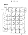
  • the following reset control is performed just before the scan is shifted from the stationary light emitting state shown in Fig. 4 to a next state where the devices E 2,2 and E 3,2 perform the light emission. That is, as shown in Fig. 5, all of the drive switches 6 1 to 6 m are turned off, all of the scan switches 5 1 to 5 n and all of the shunt switches 7 1 to 7 m are switched to the ground potential side of 0V, and all of the anode lines A 1 to A m and the cathode lines B 1 to B n are once shunted to the ground potential side of 0V, thereby all-resetting them.
  • the voltage levels of the cathode lines and anode lines in the operations shown in Figs. 4 to 6 are shown by a timing chart of Fig. 7.
  • a scanning period j the voltage across each of the devices existing on the crossing points of the cathode line B 1 and anode lines A 1 and A 2 is set to an anode line voltage level V AA (equal to V e in Figs. 4 to 6) and the light emission is performed at the luminance corresponding to the anode line voltage level V AA .
  • the grounding operation is performed as shown in Fig. 8 until the period is shifted to the resetting period after completion of the operation corresponding to a dimmer percentage shown in Fig. 4. That is, the drive switches 6 1 and 6 2 are turned off and, at the same time, all of the shunt switches 7 1 to 7 m are switched to the ground potential side of 0V. All of the anode lines A 1 to A m , consequently, are set to the ground potential. Since the cathode line B 1 is held to the ground potential, the charges stored in the devices E 1,1 and E 2,1 are discharged along routes as shown by arrows in the diagram.
  • a driving method of a display apparatus having a plurality of driving lines and a plurality of scanning lines and a plurality of capacitive light emitting devices connected between the scanning lines and the driving lines at a plurality of crossing positions by the driving lines and the scanning lines, comprising the steps of: selecting some of the plurality of driving lines for a scanning period in a predetermined cyclic period consisting of the scanning period and a resetting period subsequent thereto, sequentially selecting one of the plurality of scanning lines, connecting current sources to the selected driving lines, and supplying a current in the forward direction to each of the capacitive light emitting devices between the selected driving lines and the selected one scanning line; and in the resetting period, applying a same electric potential to driving lines to be selected for at least a next scanning period and all of the plurality of scanning lines, thereby discharging charges of the capacitive light emitting devices between the driving lines to be selected and all of the scanning lines, wherein a length of the scanning period in the predetermined cyclic
  • Fig. 10 shows a schematic construction of a display apparatus according to an embodiment of the invention using organic electroluminescence devices as capacitive light emitting devices.
  • the display apparatus has a capacitive light emitting panel 11 and a light emission control circuit 12.
  • a plurality of organic electroluminescence devices E i,j (1 ⁇ i ⁇ m, 1 ⁇ j ⁇ n) are arranged in a matrix shape at a plurality of crossing positions of the anode lines A 1 to A m of the driving lines and the cathode lines B 1 to B n of the scanning lines and connected between the scanning lines and the driving lines.
  • the cathode line scanning circuit 13 and anode line driving circuit 14 are connected to the light emission control circuit 12.
  • the light emission control circuit 12 controls the cathode line scanning circuit 13 and anode line driving circuit 14 so as to display an image indicating the image data.
  • the light emission control circuit 12 generates a scanning line selection control signal to the cathode line scanning circuit 13 and performs a control for switching the scan switches 15 1 to 15 n in a manner such that one of the cathode lines B 1 to B n corresponding to the horizontal scanning period of the image data is selected and set to the ground potential and the inverse bias potential V cc is applied to the other cathode lines.
  • the light emission control circuit 12 executes a light emission control routine every horizontal scanning period of the pixel data that is supplied.
  • the pixel data of one horizontal scanning period is fetched (step S1).
  • Luminance information is fetched from the luminance operating unit 18 (step S2).
  • the scan selection control signal and drive control signal are generated in accordance with the pixel information shown by the fetched pixel data of one horizontal scanning period (step S3).
  • each of the non-light emitting devices E 3,2 to E m,n shown by hatched capacitor symbols is charged to a polarity as shown in the diagram.
  • the light emitting state is continued only for the driving time of T/2 of the length of the half of the scanning period T.
  • each of the non-light emitting devices E 1,1 , E 1,3 to E 1,n , E 4,1 to E m,1 , and E 4,3 to E m,n shown by hatched capacitor symbols is charged to a polarity as shown in the diagram.
  • the light emitting operation such that the cathode line B 1 is scanned to thereby allow the devices E 1,1 and E 2,1 to emit the light is executed only for the driving time T/2 and, after that, the resetting period comes.
  • the voltages across all of the devices are set to the same ground potential as mentioned above.
  • the resetting period is continued until the next B 2 scanning period is started.
  • the scan is shifted to the cathode line B 2 , thereby allowing the devices E 2,2 and E 3,2 to perform the light emission.
  • a length of the B 1 scanning period when the scan is shifted from the B 1 scanning period of the dimmer of 50 % to the B 2 scanning period and a length of the resetting period in the case of using the driving method shown in Figs. 16 to 18 are similar to those shown in Fig. 15.
  • the emission of the charges of (n+1)e occurs.
  • the discharge of the charges of (m-3)e and the charging of the charges of (m+n-2)e are similarly performed.
  • Figs. 19 to 21 show further another embodiment of the invention.
  • a construction of a display apparatus is similar to that in the embodiment shown in Figs. 10 and 16 to 18.
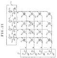
  • the reset control is performed before the scan is shifted to the state where the light emission of the next devices E 2,2 and E 3,2 is performed.
  • the drive switches 16 2 and 16 3 are switched so as to apply the bias potential V cc to the anode lines A 2 and A 3 .
  • the other drive switches 16 1 and 16 4 to 16 m relay and supply the ground potential to the anode lines A 1 and A 4 to A m .
  • All of the scan switches 15 1 to 15 n are switched to the inverse bias potential V cc side.
  • All of the anode lines A 2 and A 3 and cathode lines B 1 to B n are set to the same potential V cc .
  • the driving current flows from the current sources 17 2 and 17 3 as shown by arrows and only the devices E 2,2 and E 3,2 perform the light emission.
  • each of the non-light emitting devices E 1,1 , E 1,3 to E 1,n , E 4,1 to E m,1 , and E 4,3 to E m,n shown by hatched capacitor symbols is charged to a polarity as shown in the diagram.
  • Figs. 22 to 25 show further another embodiment of the invention.
  • a construction of a display apparatus is similar to that in the embodiment shown in Figs. 10 and 12 to 14.
  • Figs. 22 to 25 show operating states of the B 1 scanning period, resetting period, and B 2 scanning period in the case where the cathode line B 1 is scanned to thereby allow the devices E 1,1 and E 2,1 to perform the light emission by the control operation of the light emission control circuit 12 and, thereafter, the scan is shifted to the cathode line B 2 to thereby allow the devices E 2,2 and E 3,2 to perform the light emission, respectively.
  • the luminance information obtained from the from the luminance operating unit 18 at the time shows the dimmer of 50 % and, further, a gradation ratio of the devices E 1,1 and E 2,1 is equal to 1 : 1 ⁇ 2 in the dimmer of 50 %.
  • the operating states will now be described.
  • each of the non-light emitting devices E 3,2 to E m,n shown by hatched capacitor symbols is charged to a polarity as shown in the diagram.
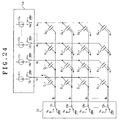
  • the reset control is performed. All of the drive switches 16 1 to 16 m and the scan switches 15 1 to 15 n are switched to the ground potential side of 0V as shown in Fig. 24 and all of the anode lines A 1 to A m and cathode lines B 1 to B n are set to the same ground potential of 0V.
  • the reset control since all of the anode lines and cathode lines are set to the same electric potential of 0V, the charges stored in each device are discharged along routes as shown by arrows in the diagram. The stored charges of all of the devices are instantaneously extinguished.
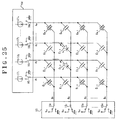
  • the driving current flows from the current sources 17 2 and 17 3 as shown by arrows and only the devices E 2,2 and E 3,2 perform the light emission.
  • each of the non-light emitting devices E 1,1 , E 1,3 to E 1,n , E 4,3 to E m,1 , and E 4,3 to E m,n shown by hatched capacitor symbols is charged to a polarity as shown in the diagram.
  • the light emitting operation for scanning the cathode line B 1 and allowing the devices E 1,1 and E 2,1 to perform the light emission is executed only for the former half driving time of T/4, and the light emitting operation for allowing only the device E 1,1 to perform the light emission is executed only for the latter half driving time of T/4.
  • a gradation ratio of the devices E 1,1 and E 2,1 is, thus, equal to 1 : 1 ⁇ 2.
  • the voltages across all of the devices are set to the same ground potential. The resetting period is continued until the next B 2 scanning period is started.
  • the scan is shifted to the cathode line B 2 to thereby allow the devices E 2,2 and E 3,2 to perform the light emission.
  • the emission of the charges of e and the charging of the charges of (n-1)e occur.
  • shifting from the B 1 scanning period to the resetting period the emission of the charges of (m-1)(n-1)e + e occurs.
  • the charging of the charges of [2 + (m-2)(n-1)]e is similarly performed.
  • the electric potentials which are applied to the driving lines and scanning lines are not limited to the ground potential and bias potential V cc .

Landscapes

  • Engineering & Computer Science (AREA)
  • Physics & Mathematics (AREA)
  • Computer Hardware Design (AREA)
  • General Physics & Mathematics (AREA)
  • Theoretical Computer Science (AREA)
  • Control Of Indicators Other Than Cathode Ray Tubes (AREA)
  • Control Of El Displays (AREA)
  • Electroluminescent Light Sources (AREA)

Abstract

A display apparatus using capacitive light emitting devices, in which some of a plurality of driving lines are selected in a scanning period in predetermined cyclic period consisting of the scanning period and a resetting period subsequent thereto, current sources are connected to the selected driving lines, and a current in the forward direction is supplied to each of the capacitive light emitting devices between the selected driving lines and a selected one scanning line, and in the resetting period, a same electric potential is applied to driving lines to be selected for a next scanning period and all of the plurality of scanning lines, thereby discharging charges of the capacitive light emitting devices between the driving lines to be selected and all of the scanning lines, wherein a length of the scanning period in the predetermined cyclic period is changed in response to a luminance information command, and the period other than the scanning period in the predetermined cyclic period is set to the resetting period.

Description

BACKGROUND OF THE INVENTION 1. Field of the Invention
The invention relates to a display apparatus using capacitive light emitting devices such as organic electroluminescence devices or the like and its driving method.
2. Description of the Related Art
As a display in which an electric power consumption is low and a display quality is high and, further, a thin size can be realized, an electroluminescence display constructed by arranging a plurality of organic electroluminescence devices in a matrix shape is highlighted. As shown in Fig. 1, the organic electroluminescence device is constructed in a manner such that an organic function layer 102 of at least one layer consisting of an electron transporting layer, a light emitting layer, a hole transporting layer, or the like and a metal electrode 103 are laminated on a transparent substrate 100 made of a glass substrate or the like on which a transparent electrode 101 is formed. When a plus voltage is applied to an anode of the transparent electrode 101 and a minus voltage is applied to a cathode of the metal electrode 103, namely, when a direct current is applied across the transparent electrode and the metal electrode, the organic function layer 102 emits light. An organic compound in which good light emitting characteristics can be expected is used as an organic function layer, thereby enabling the electroluminescence display to endure a practical use.
The organic electroluminescence device (hereinafter, simply referred to as a device) can be electrically expressed by an equivalent circuit as shown in Fig. 2. As will be understood from the diagram, the device can be replaced with a construction comprising a capacitance component C and a component E of characteristics of a diode connected in parallel to the capacitance component. The organic electroluminescence device is, therefore, regarded as a capacitive light emitting device. According to the organic electroluminescence device, when a DC light emission driving voltage is applied across the electrodes, charges are stored in the capacitance component C. Subsequently, when the applied voltage exceeds a barrier voltage or a light emission threshold voltage that is peculiar to the device, a current starts on flowing to the organic function layer serving as a light emitting layer from the electrode (anode side of the diode component E) and the device emits the light at an intensity which is proportional to the current.
The characteristics of a voltage V - a current I - a luminance L of the device are similar to those of the diode as shown in Fig. 3. When the device is supplied with a voltage of a light emission threshold value Vth or less, the current I is extremely small. When the voltage exceeds the light emission threshold value Vth, the current I suddenly increases. The current I is almost proportional to the luminance L. According to the device, if a driving voltage exceeding the light emission threshold value Vth is applied to the device, the light emission luminance proportional to the current according to the driving voltage is provided. If the driving voltage applied is equal to or less than the light emission threshold value Vth, no driving current flows and the light emission luminance is equal to zero.
A simple matrix driving system can be applied as a driving method of a display panel using a plurality of organic electroluminescence devices. Fig. 4 shows a structure of an example of a simple matrix display panel. n cathode lines (metal electrodes) B1 to Bn are extended and provided in parallel in the lateral direction and m anode lines (transparent electrodes) A1 to Am are extended and provided in parallel in the vertical direction. Light emitting layers of organic electroluminescence devices E1,1 to Em,n are sandwiched in (total n × m) crossing portions of the cathode lines and the anode lines. The devices E1,1 to Em,n serving as pixels are arranged in a lattice shape. In correspondence to each crossing position of the anode lines A1 to Am in the vertical direction and the cathode lines B1 to Bn in the horizontal direction, one end (anode line side of the diode component E of the equivalent circuit) is connected to the anode line and the other end (cathode line side of the diode component E of the equivalent circuit) is connected to the cathode line. The cathode lines are connected to a cathode line scanning circuit 1. The anode lines are connected to an anode line driving circuit 2.
The cathode line scanning circuit 1 has scan switches 51 to 5n corresponding to the cathode lines B1 to Bn in which an electric potential of each cathode line is individually determined. Each scan switch applies either an inverse bias potential Vcc (for example, 10V) which is obtained from a power voltage or a ground potential (0V) to the corresponding cathode line.
The anode line driving circuit 2 has current sources 21 to 2m (for example, constant current sources) and drive switches 61 to 6m corresponding to the anode lines A1 to Am for individually supplying a driving current to each device through each anode line and is constructed in a manner such that the drive switch is on/off controlled so as to individually supply a current to each anode line. A voltage source such as a constant voltage source can be also used as a driving source. A current source (power supplying circuit whose supply current amount is controlled so as to have a desired value) is generally used because of reasons such that voltage - luminance characteristics are unstable for a temperature change although the current - luminance characteristics are stable for a temperature change and the like. The supply current amount of each of the current sources 21 to 2m is set to a current amount that is necessary to maintain a state where the device emits the light at a desired instantaneous luminance (hereinafter, the state is referred to as a stationary light emitting state). When the device is in the stationary light emitting state, the charges corresponding to the supply current amount are stored in the capacitance component C of the device. Thus, a voltage across the device is equal to a specified value Ve (hereinafter, referred to as a specified light emission voltage) corresponding to the instantaneous luminance.
The anode lines are also connected to an anode line resetting circuit 3. The anode line resetting circuit 3 has shunt switches 71 to 7m provided every anode line. When the shunt switch is selected, the corresponding anode line is set to a ground potential.
The cathode line scanning circuit 1, anode line driving circuit 2, and anode line resetting circuit 3 are connected to a light emission control circuit 4.
The light emission control circuit 4 controls the cathode line scanning circuit 1, anode line driving circuit 2, and anode line resetting circuit 3 in accordance with image data supplied from an image data generating system (not shown) so as to display an image shown by the image data. The light emission control circuit 4 generates a scanning line selection control signal to the cathode line scanning circuit 1 and controls so as to switch the scan switches 51 to 5n in a manner such that one of the cathode lines corresponding to a horizontal scanning period of the image data is selected and set to the ground potential and the inverse bias potential Vcc is applied to the other cathode lines. The inverse bias potential Vcc is applied by the constant voltage source connected to the cathode line in order to prevent that the device connected to the crossing point of the anode line which is at present being driven and the cathode line in which a scan selection is not performed emits light due to crosstalk. The inverse bias potential Vcc is generally set so that Vcc = specified light emission voltage Ve. Since the scan switches 51 to 5n are sequentially switched to the ground potential every horizontal scanning period, the cathode line set to the ground potential functions as a scanning line which enables the device connected to the cathode line to emit light.
The anode line driving circuit 2 executes a light emission control to the scanning line. The light emission control circuit 4 generates a drive control signal (driving pulse) showing which one of the devices connected to the scanning line is allowed to emit light at which timing and how long in accordance with the pixel information shown by the image data and supplies it to the anode line driving circuit 2. In response to the drive control signal, the anode line driving circuit 2 on/off controls some of the drive switches 61 to 6m and supplies a driving current to the devices according to the pixel information through the anode lines A1 to Am. The device to which the driving current was supplied emits light in accordance with the pixel information.
The resetting operation of the anode line resetting circuit 3 is executed in response to the reset control signal from the light emission control circuit 4. The anode line resetting circuit 3 turns on any switches of the shunt switches 71 to 7m corresponding to the anode line as a reset target shown by the reset control signal and turns off the other shunt switches.
A driving method of performing the resetting operation to discharge the charges stored in each device arranged in the lattice shape just before the scanning lines in the simple matrix display panel (hereinafter, referred to as a reset driving method) is disclosed in JP-A-9-232074 filed by the same applicant as that of the present invention. The reset driving method intends to makes a timing for activating the light emission of the device when the scanning line is switched early. The reset driving method of the simple matrix display panel will be described with reference to Figs. 4 to 6.
The operations shown in Figs. 4 to 6, which will be explained hereinlater, relates to the case where after the cathode line B1 was scanned and the devices E1,1 and E2,1 were lit on, the cathode line B2 is scanned and the devices E2,2 and E3,2 are lit on as an example. For making the description easy, the lit-on device is shown by a diode symbol and the lit-off light emitting device is shown by a capacitor symbol. The inverse bias potential Vcc which is applied to the cathode lines B1 to Bn is set to 10V that is the same as the specified light emission voltage Ve of the device.
First, in Fig. 4, only the scan switch 51 is switched to the ground potential side of 0V and the cathode line B1 is scanned. The inverse bias potential Vcc is applied to the other cathode lines B2 to Bn by the scan switches 52 to 5n. At the same time, the current sources 21 and 22 are connected to the anode lines A1 and A2 by the drive switches 61 and 62. The other anode lines A3 to Am are switched to the ground potential side of 0V by the shunt switches 73 to 7m. In the case of Fig. 4, therefore, only the devices E1,1 and E2,1 are biased in the forward direction, the driving current flows from the current sources 21 and 22 as shown by arrows, and only the devices E1,1 and E2,1 perform the light emission. In the state, each of the non-light emitting devices E3,2 to Em,n shown by hatched capacitor symbols is charged to a polarity as shown in the diagram.
The following reset control is performed just before the scan is shifted from the stationary light emitting state shown in Fig. 4 to a next state where the devices E2,2 and E3,2 perform the light emission. That is, as shown in Fig. 5, all of the drive switches 61 to 6m are turned off, all of the scan switches 51 to 5n and all of the shunt switches 71 to 7m are switched to the ground potential side of 0V, and all of the anode lines A1 to Am and the cathode lines B1 to Bn are once shunted to the ground potential side of 0V, thereby all-resetting them. When the all-resetting operation is performed, since all of the anode lines and the cathode lines are set to the same electric potential of 0V, the charges stored in each device are discharged along routes shown by arrows in the diagram and the stored charges of all devices are instantaneously extinguished.
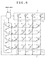
After the stored charges of all devices are set to zero as mentioned above, only the scan switch 52 corresponding to the cathode line B2 is subsequently switched to the 0V side as shown in Fig. 6 and the cathode line B2 is scanned. At the same time, the drive switches 62 and 63 are closed, the current sources 22 and 23 are connected to the corresponding anode lines, the shunt switches 71 and 74 to 7m are turned on, and 0V is applied to the anode lines A1 and A4 to Am.
As mentioned above, in the light emission control of the reset driving method, a scan mode serving as a period of time during which one of the cathode lines B1 to Bn is made active and a subsequent reset mode are repeated. The scan mode and the reset mode are executed every horizontal scanning period (1H) of the image data. Now, assuming that the control mode is directly shifted from the state of Fig. 4 to the state of Fig. 6 without performing the reset control, for example, the driving current which is supplied from the current source 23 not only flows into the device E3,2 but also is expended to cancel the reverse direction charges (shown in Fig. 4) stored in the devices E3,3 to E3,n, so that it takes time to set the device E3,2 into the stationary light emitting state (the voltage across the device E3,2 to the specified light emission voltage Ve).
When the reset control is performed, however, since the potentials of the anode lines A2 and A3 are set to approximately Vcc at a moment when the scan is switched to the scan of the cathode line B2, the charging currents are supplied to the devices E2,2 and E3,2 to be subsequently lit on from not only the current sources 22 and 23 but also a plurality of routes from the constant voltage sources connected to the cathode lines B1 and B3 to Bn. A parasitic capacitance is charged by the charging currents, the voltage instantaneously reaches the specified light emission voltage Ve and the device can be instantaneously shifted to the stationary light emitting state. After that, within the scanning period of the cathode line B2, since an amount of current which is supplied from the current source as mentioned above is set to a current amount such that device can maintain the stationary light emitting state at the specified light emission voltage Ve, the currents which are supplied from the current sources 22 and 23 flow into only the devices E2,2 and E3,2 and all of them are expended for light emission. That is, the light emitting state shown in Fig. 6 is continued.
According to the conventional reset driving method as mentioned above, since all of the cathode lines and anode lines are once connected to 0V as a ground potential or the same electric potential of the inverse bias potential Vcc and reset before the control mode is shifted to the light emission control of the next scanning line, when the scanning line is switched to the next scanning line, the charging time until the specified light emission voltage Ve is shortened and the activating speed of the light emission of the device to perform the light emission on the switched scanning line can be made fast.
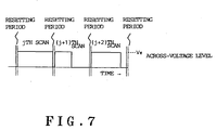
The voltage levels of the cathode lines and anode lines in the operations shown in Figs. 4 to 6 are shown by a timing chart of Fig. 7. In a scanning period j, the voltage across each of the devices existing on the crossing points of the cathode line B1 and anode lines A1 and A2 is set to an anode line voltage level VAA (equal to Ve in Figs. 4 to 6) and the light emission is performed at the luminance corresponding to the anode line voltage level VAA. In a next scanning period j+1, the voltage across each of the devices existing on the crossing points of the cathode line B2 and anode lines A2 and A3 is set to an anode line voltage level VAA (equal to Ve in Figs. 4 to 6) and the light emission is performed at the luminance corresponding to the anode line voltage level VAA.
In the light emission display using the conventional reset driving method mentioned above, in the case of performing the luminance adjustment, a general luminance adjusting method of the matrix display is applied. That is, as shown in Fig. 7, there is a method whereby the level of the voltage across the device at the time of the light emission is set to a constant value (that is, the constant instantaneous luminance and constant driving current of the device) and a connecting time of a driving source to the anode line is changed within a range of the scanning period of time, thereby adjusting the light emission luminance of each device (pulse width modulating method).
That is, if a luminance gradation (dimmer) is applied in dependence on a length of the driving time within each scanning period, the scanning period j in Fig. 7 relates to the case of the dimmer of 100 % in which the luminance is the maximum because the light emitting state is continued until the end of the period. The scanning period j+1 relates to the case of the dimmer of 50 % because the light emitting state is continued until the time point of the half of the period. The scanning period j+2 relates to the case of the dimmer of 80 % because the light emitting state is continued until the time point of 80 % of the period.
Within the scanning period in the cases other than the dimmer of 100 %, the grounding operation is performed as shown in Fig. 8 until the period is shifted to the resetting period after completion of the operation corresponding to a dimmer percentage shown in Fig. 4. That is, the drive switches 61 and 62 are turned off and, at the same time, all of the shunt switches 71 to 7m are switched to the ground potential side of 0V. All of the anode lines A1 to Am, consequently, are set to the ground potential. Since the cathode line B1 is held to the ground potential, the charges stored in the devices E1,1 and E2,1 are discharged along routes as shown by arrows in the diagram. The stored charges of the devices E1,1 and E2,1 are instantaneously extinguished. Since the cathode lines B2 to Bn are held in a state where the inverse bias potential Vcc was applied by the scan switches 52 to 5n, in the state, each of the non-light emitting devices E1,2 to E1,n, E2,2 to E2,n, ..., and Em,2 to Em,n shown as hatched capacitor symbols in Fig. 8 is charged to a polarity as shown in the diagram or maintains the charging state by the polarity. When the resetting period comes after that, the operation shown in Fig. 5 is executed.
In the B1 scanning period of the dimmer of 100 %, as shown in Fig. 9A, after the cathode line B1 was scanned and the devices E1,1 and E2,1 were lit on, in the case where the scan is shifted to the cathode line B2 in the resetting period and the next B2 scanning period and the devices E2,2 and E3,2 are lit on, the emission of the charges of [2 + (m-2)(n-1)]e occurs in the resetting period. The charging of the charges of [2 + (m-2)(n- 1)]e is performed in the B2 scanning period. Now, assuming that m = 4 for easy understanding, an emission amount of the charges in the resetting period is equal to 2ne and a charging amount of the charges in the B2 scanning period is equal to 2ne.
In the B1 scanning period of the dimmer of 50 %, as shown in Fig. 9B, the light emitting operation for scanning the cathode line B1 and allowing the devices E1,1 and E2,1 to be lit on and the grounding operation to connect them to the ground by the shunt switches 71 to 7m as mentioned above are sequentially performed by an amount of 50 % at a time. After that, the scan is shifted to the cathode line B2 in the resetting period and the next B2 scanning period and the devices E2,2 and E3,2 are lit on. In the case, the emission of the charges of 2e and the charging of the charges of (m-2)(n-1)e are performed in the grounding operation within the B1 scanning period. The emission of the charges of (m-2)(n-1)e occurs in the resetting period. The charging of the charges of [2 + (m-2)(n-1)]e is similarly performed in the B2 scanning period. Now, assuming that m = 4, a charging amount of the charges in the grounding operation in the B1 scanning period is equal to 2(n-1)e, an emission amount of the charges in the resetting period is equal to 2(n-1)e and a charging amount of the charges in the B2 scanning period is equal to 2ne.
There is a problem such that in the case of getting the intermediate luminance in which the grounding operation is included in the scanning period like the case of the dimmer of 50 %, an invalid electric power consumption is larger than that in the case of the maximum luminance of the dimmer of 100 %.
OBJECTS AND SUMMARY OF THE INVENTION
It is, therefore, an object of the invention to provide a display apparatus of capacitive light emitting devices which can reduce an electric power consumption in the case of a gradation display and an intermediate luminance and to provide its driving method.
According to the invention, there is provided a driving method of a display apparatus having a plurality of driving lines and a plurality of scanning lines and a plurality of capacitive light emitting devices connected between the scanning lines and the driving lines at a plurality of crossing positions by the driving lines and the scanning lines, comprising the steps of: selecting some of the plurality of driving lines for a scanning period in a predetermined cyclic period consisting of the scanning period and a resetting period subsequent thereto, sequentially selecting one of the plurality of scanning lines, connecting current sources to the selected driving lines, and supplying a current in the forward direction to each of the capacitive light emitting devices between the selected driving lines and the selected one scanning line; and in the resetting period, applying a same electric potential to driving lines to be selected for at least a next scanning period and all of the plurality of scanning lines, thereby discharging charges of the capacitive light emitting devices between the driving lines to be selected and all of the scanning lines, wherein a length of the scanning period in the predetermined cyclic period is changed in response to a luminance information command indicative of a display luminance, and the period other than the scanning period in the predetermined cyclic period is set to the resetting period.
According to the invention, there is provided a display apparatus comprising: a plurality of driving lines and a plurality of scanning lines; a plurality of capacitive light emitting devices connected between the scanning lines and the driving lines at a plurality of crossing positions by the driving lines and the scanning lines; scanning period control means for selecting some of the plurality of driving lines in a scanning period in a predetermined cyclic period consisting of the scanning period and a resetting period subsequent thereto, sequentially selecting one of the plurality of scanning lines, connecting current sources to the selected driving lines, and supplying a current in the forward direction to each of the capacitive light emitting devices between the driving lines to be selected and the selected one scanning line; and resetting period control means for applying a same electric potential to driving lines to be selected for at least a next scanning period and all of the plurality of scanning lines in the resetting period, thereby discharging charges of the capacitive light emitting devices between the driving lines to be selected and all of the scanning lines, wherein a length of the scanning period in the predetermined cyclic period is changed in response to a luminance information command indicative of a display luminance, and the period other than the scanning period in the predetermined cyclic period is set to the resetting period.
BRIEF DESCRIPTION OF THE DRAWINGS
  • Fig. 1 is a cross sectional view of an organic electroluminescence device;
  • Fig. 2 is a diagram showing an equivalent circuit of the organic electroluminescence device;
  • Fig. 3 is a diagram schematically showing characteristics of a driving voltage - a current - a light emission luminance of the organic electroluminescence device;
  • Fig. 4 is a block diagram for explaining a reset driving method which is applied to a display apparatus using conventional organic electroluminescence devices;
  • Fig. 5 is a block diagram for explaining a reset driving method which is applied to the display apparatus using the conventional organic electroluminescence devices;
  • Fig. 6 is a block diagram for explaining a reset driving method which is applied to the display apparatus using the conventional organic electroluminescence devices;
  • Fig. 7 is a diagram for explaining a luminance adjustment of the display apparatus using the conventional organic electroluminescence devices;
  • Fig. 8 is a block diagram for explaining a reset driving method in the case where the grounding operation is included in a scanning period;
  • Figs. 9A and 9B are diagrams showing timing charts of a conventional reset driving method;
  • Fig. 10 is a block diagram showing a schematic construction of a display apparatus according to the invention;
  • Fig. 11 is a flowchart showing a light emission control routine which is executed by a light emission control circuit;
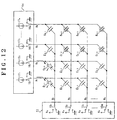
  • Fig. 12 is a block diagram for explaining a reset driving method which is applied to the display apparatus of Fig. 10;
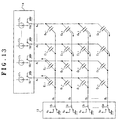
  • Fig. 13 is a block diagram for explaining a reset driving method which is applied to the display apparatus of Fig. 10;
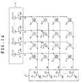
  • Fig. 14 is a block diagram for explaining a reset driving method which is applied to the display apparatus of Fig. 10;
  • Fig. 15 is a diagram showing a timing chart of the reset driving methods shown in Figs. 12 to 14;
  • Fig. 16 is a block diagram for explaining a reset driving method which is applied to the display apparatus of Fig. 10;
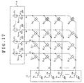
  • Fig. 17 is a block diagram for explaining a reset driving method which is applied to the display apparatus of Fig. 10;
  • Fig. 18 is a block diagram for explaining a reset driving method which is applied to the display apparatus of Fig. 10;
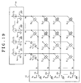
  • Fig. 19 is a block diagram for explaining a reset driving method which is applied to the display apparatus of Fig. 10;
  • Fig. 20 is a block diagram for explaining a reset driving method which is applied to the display apparatus of Fig. 10;
  • Fig. 21 is a block diagram for explaining a reset driving method which is applied to the display apparatus of Fig. 10;
  • Fig. 22 is a block diagram for explaining a reset driving method which is applied to the display apparatus of Fig. 10;
  • Fig. 23 is a block diagram for explaining a reset driving method which is applied to the display apparatus of Fig. 10;
  • Fig. 24 is a block diagram for explaining a reset driving method which is applied to the display apparatus of Fig. 10;
  • Fig. 25 is a block diagram for explaining a reset driving method which is applied to the display apparatus of Fig. 10; and
  • Fig. 26 is a diagram showing a timing chart of the reset driving methods shown in Figs. 22 to 25.
  • DETAILED DESCRIPTION OF THE PREFERRED EMBODIMENTS
    An embodiment of the invention will now be described in detail hereinbelow with reference to the drawings.
    Fig. 10 shows a schematic construction of a display apparatus according to an embodiment of the invention using organic electroluminescence devices as capacitive light emitting devices. The display apparatus has a capacitive light emitting panel 11 and a light emission control circuit 12.
    In the light emitting panel 11, in a manner similar to that shown in Figs. 4 to 6 and 8, a plurality of organic electroluminescence devices Ei,j (1 ≤ i ≤ m, 1 ≤ j ≤ n) are arranged in a matrix shape at a plurality of crossing positions of the anode lines A1 to Am of the driving lines and the cathode lines B1 to Bn of the scanning lines and connected between the scanning lines and the driving lines. That is, the organic electroluminescence devices are arranged at crossing positions of a plurality of driving lines which are extended almost in parallel and a plurality of scanning lines which are extended in parallel and each of which is extended almost perpendicularly to each of the driving lines and are connected to the scanning lines and the driving lines, respectively.
    A cathode line scanning circuit 13 serving as scan switch means and an anode line driving circuit 14 serving as drive switch means are connected to the light emitting panel 11. The cathode line scanning circuit 13 enables scanning lines to be freely connected to either one of different electric potentials, for example, a ground potential and an inverse bias potential. The anode line driving circuit 14 enables the driving lines to be freely connected to at least one of the ground potential and the inverse bias potential or to a driving source. Although the cathode line scanning circuit 13 is constructed in a manner similar to that shown in Figs. 4 to 6 and 8, the anode line driving circuit 14 also includes the function of the anode line resetting circuit 3 shown in Figs. 4 to 6 and 8.
    As shown in Figs. 12 to 14, the cathode line scanning circuit 13 has scan switches 151 to 15n corresponding to the cathode lines B1 to Bn and each scan switch applies one of the inverse bias potential Vcc consisting of a power voltage and the ground potential to the corresponding cathode line. The anode line driving circuit 14 has drive switches 161 to 16m for switching to either current sources 171 to 17m corresponding to the anode lines A1 to Am or the ground potential and performs a switching control so that each of the drive switches 161 to 16m supplies a current to the anode line.
    The cathode line scanning circuit 13 and anode line driving circuit 14 are connected to the light emission control circuit 12.
    In accordance with image data supplied from an image data generating system (not shown), the light emission control circuit 12 controls the cathode line scanning circuit 13 and anode line driving circuit 14 so as to display an image indicating the image data. The light emission control circuit 12 generates a scanning line selection control signal to the cathode line scanning circuit 13 and performs a control for switching the scan switches 151 to 15n in a manner such that one of the cathode lines B1 to Bn corresponding to the horizontal scanning period of the image data is selected and set to the ground potential and the inverse bias potential Vcc is applied to the other cathode lines. The inverse bias potential Vcc is applied by the constant voltage source connected to the cathode line in order to prevent that the device connected to the crossing point of the anode line which is at present being driven and the cathode line in which a scan selection is not performed emits light due to crosstalk. Since the scan switches 151 to 15n have sequentially switched to the ground potential every horizontal scanning period, the cathode lines B1 to Bn set to the ground potential function as scanning lines for enabling the devices connected to the cathode lines to perform the light emission.
    The light emission control circuit 12 generates a drive control signal (driving pulse) showing which ones of the devices connected to the scanning lines are made to perform the light emission at which timing and how long in accordance with the pixel information shown by the image data and supplies it to the anode line driving circuit 14. In response to the drive control signal, the anode line driving circuit 14 switches the drive switches corresponding to the light emission among the drive switches 161 to 16m to the current source side, supplies a driving current to the relevant devices according to the pixel information through the corresponding ones of the anode lines A1 to Am, and supplies the ground potential to the other anode lines through the drive switches.
    A luminance operating unit 18 is connected to the light emission control circuit 12. The luminance operating unit 18 can be operated to adjust a display luminance of the light emitting panel 11 and generates luminance information (percentage of the dimmer) according to the operating position of the user to the light emission control circuit 12.
    A driving method of the capacitive light emitting panel in the light emission control circuit 12 will now be described with reference to a flowchart of Fig. 11.
    The light emission control circuit 12 executes a light emission control routine every horizontal scanning period of the pixel data that is supplied. In the light emission control routine, first, the pixel data of one horizontal scanning period is fetched (step S1). Luminance information is fetched from the luminance operating unit 18 (step S2). The scan selection control signal and drive control signal are generated in accordance with the pixel information shown by the fetched pixel data of one horizontal scanning period (step S3).
    The scan selection control signal is supplied to the cathode line scanning circuit 13. In order to set one of the cathode lines B1 to Bn corresponding to the present horizontal scanning period shown by the scan selection control signal to the ground potential, the cathode line scanning circuit 13 switches the scan switch (one scan switch 15S among the scan switches 151 to 15n : S denotes one of 1 to n) corresponding to the relevant one cathode line to the grounding side. The scan switches (all of the scan switches other than the one scan switch 15S among the scan switches 151 to 15n) are switched to the grounding side in order to apply the inverse bias potential Vcc to the other cathode lines.
    The drive control signal is supplied to the anode line driving circuit 14. The anode line driving circuit 14 switches the drive switches (any ones of the drive switches 161 to 16m) corresponding to the anode lines including the devices to be driven so as to perform the light emission among the anode lines A1 to Am within the present horizontal scanning period shown by the drive control signal to the current source (corresponding ones of 171 to 17m) side. The other anode lines are switched to the grounding side. For example, consequently, when the drive switch 161 is switched to the current source 171 side, the driving current flows from the current source 171 to the drive switch 161, anode line A1, device E1,S, cathode line BS, scan switch 15S, and the ground. The device E1,S to which the driving current has been supplied performs the light emission according to the pixel information.
    The light emission control circuit 12 discriminates whether the driving time corresponding to the fetched luminance information has elapsed after the execution of step S3 or not (step S4). For a predetermined horizontal scanning period T, a length corresponding to the percentage of the dimmer shown by the fetched luminance information becomes the driving time. For example, when the fetched luminance information indicates the dimmer of 100 %, the length of the scanning period T becomes the driving time as it is. When it indicates the dimmer of 50 %, the length of the half (namely, T/2) of the scanning period T becomes the driving time. Within the driving time, the light emission of the device driven by the generation of the scan selection control signal and drive control signal in step S3 is continued. The measurement of the driving time is executed by an internal counter (not shown).
    When the driving time elapses, the light emission control circuit 12 generates a reset signal (step S5). The reset signal is supplied to the cathode line scanning circuit 13 and anode line driving circuit 14. The cathode line scanning circuit 13 switches movable contacts of all of the scan switches 151 to 15n to the grounding side fixed contacts in response to the reset signal. The anode line driving circuit 14 switches movable contacts of all of the drive switches 161 to 16n to the grounding side fixed contacts in response to the reset signal. The voltages across all of the devices Ei,j are set to the ground potential, thereby discharging charges stored in the devices.
    After completion of the execution of step S5, the light emission control circuit 12 finishes the light emission control routine and waits until the next horizontal scanning period is started. The resetting operation in step S5 is continued for a period of time until the next horizontal scanning period is started. When the next horizontal scanning period is started, the operations in steps S1 to S5 are repeated.
    The case where the cathode line B1 is scanned by the control operation of the light emission control circuit 12 and the devices E1,1 and E2,1 are lit on and, after that, the scan is shifted to the cathode line B2 and the devices E2,2 and E3,2 are lit on will now be described with reference to Figs. 12 to 14. It is assumed that the luminance information obtained from the luminance operating unit 18 at the time shows the dimmer of 50 %. In Figs. 12 to 14, to make it easy to explain in a manner similar to the case of Figs. 4 to 6, the lit-on device is shown by the diode symbol and the lit-off light emitting device is shown by a capacitor symbol.
    First, in Fig. 12, only the scan switch 151 is switched to the ground potential side of 0V and the cathode line B1 is scanned. The inverse bias potential Vcc is applied to the other cathode lines B2 to Bn by the scan switches 152 to 15n. At the same time, the current sources 171 and 172 are connected to the anode lines A1 and A2 by the drive switches 161 and 162. The other anode lines A3 to Am are switched to the ground potential side of 0V by the drive switches 163 to 16m. In the case of Fig. 12, therefore, only the devices E1,1 and E2,1 are biased in the forward direction, the driving current flows from the current sources 171 and 172 as shown by arrows, and only the devices E1,1 and E2,1 perform the light emission. In the light emitting state, each of the non-light emitting devices E3,2 to Em,n shown by hatched capacitor symbols is charged to a polarity as shown in the diagram. The light emitting state is continued only for the driving time of T/2 of the length of the half of the scanning period T.
    When the driving time T/2 elapses from the stationary light emitting state of Fig. 12, the reset control is performed before the scan is shifted to the state where the light emission of the next devices E2,2 and E3,2 is performed. As shown in Fig. 13, all of the drive switches 161 to 16m and all of the scan switches 151 to 15n are switched to the ground potential side of 0V and all of the anode lines A1 to Am and cathode lines B1 to Bn are set to the same ground potential of 0V. By the reset control, since all of the anode lines and cathode lines are set to the same electric potential of 0V, the charges stored in each device are discharged along routes as shown by arrows in the diagram. The stored charges of all of the devices are instantaneously extinguished.
    After the stored charges of all devices were set to zero in the manner, when the next horizontal scanning period is started, subsequently, as shown in Fig. 14, only the scan switch 152 corresponding to the cathode line B2 is switched to the 0V side and the cathode line B2 is scanned. At the same time, the drive switches 162 and 163 are switched to the side of the current sources 172 and 173 and connected to the corresponding anode lines. Also, the other drive switches 161 and 164 to 16m are held in a state where they were switched to the ground potential side, and 0V is applied to the anode lines A1 and A4 to Am. In the case of Fig. 14, therefore, only the devices E2,2 and E3,2 are biased in the forward direction, the driving current flows from the current sources 172 and 173 as shown by arrows, and only the devices E2,2 and E3,2 perform the light emission. In the light emitting state, each of the non-light emitting devices E1,1, E1,3 to E1,n, E4,1 to Em,1, and E4,3 to Em,n shown by hatched capacitor symbols is charged to a polarity as shown in the diagram.
    In the B1 scanning period of the dimmer of 50 %, as shown in Fig. 15, the light emitting operation such that the cathode line B1 is scanned to thereby allow the devices E1,1 and E2,1 to emit the light is executed only for the driving time T/2 and, after that, the resetting period comes. In the resetting period, the voltages across all of the devices are set to the same ground potential as mentioned above. The resetting period is continued until the next B2 scanning period is started. In the B2 scanning period, the scan is shifted to the cathode line B2, thereby allowing the devices E2,2 and E3,2 to perform the light emission. In the case, when the B1 scanning period is shifted to the resetting period, the emission of the charges of [2 + (m-2)(n-1)]e occurs. In the B2 scanning period, the charging of the charges of [2 + (m-2)(n-1)]e is similarly performed. Now, assumed that m = 4 to make the explanation easy, the emission amount of the charges in the resetting period is equal to 2ne and the charging amount of the charges in the B2 scanning period is equal to 2ne. That is, the charges of 4ne are consumed as a whole by the operations of Figs. 12 to 14 and an amount of charges to be consumed can be reduced to a value lower than that by the conventional reset driving method.
    Figs. 16 to 18 show another embodiment of the invention. In the embodiment, each of the drive switches 161 to 16m in the anode line driving circuit 14 of the display apparatus has three fixed contacts. The bias potential Vcc is applied to the first fixed contact. The current source (one of 171 to 17m) is connected to the second fixed contact. The third fixed contact is connected to the ground. The movable contact of each of the drive switches 161 to 16m is connected to one of the first to third fixed contacts in response to the drive control signal or reset signal from the light emission control circuit 12. The other construction is similar to that shown in Figs. 10 and 12 to 14.
    Figs. 16 to 18 show operating states of the B1 scanning period, resetting period, and B2 scanning period in the case where the cathode line B1 is scanned to thereby allow the devices E1,1 and E2,1 to perform the light emission by the control operation of the light emission control circuit 12 and, after that, the scan is shifted to the cathode line B2 to thereby allow the devices E2,2 and E3,2 to perform the light emission, respectively. It is assumed that the luminance information obtained from the luminance operating unit 18 at the time is equal to a dimmer of 50 %. The operating states will now be described.
    First, in Fig. 16, only the scan switch 151 is switched to the ground potential side of 0V and the cathode line B1 is scanned. The inverse bias potential Vcc is applied to the other cathode lines B2 to Bn by the scan switches 152 to 15n. At the same time, the current sources 171 and 172 are connected to the anode lines A1 and A2 by the drive switches 161 and 162. The other anode lines A3 to Am are switched to the ground potential side of 0V by the drive switches 163 to 16m. In the case of Fig. 16, therefore, only the devices E1,1 and E2,1 are biased in the forward direction, the driving current flows from the current sources 171 and 172 as shown by arrows, and only the devices E1,1 and E2,1 perform the light emission. In the light emitting state, each of the non-light emitting devices E3,2 to Em,n shown by hatched capacitor symbols is charged to a polarity as shown in the diagram. The light emitting state is continued only for the driving time of T/2 of the length of the half of the scanning period T.
    When the driving time T/2 elapses from the stationary light emitting state of Fig. 16, the reset control is performed before the scan is shifted to the state where the light emission of the next devices E2,2 and E3,2 is performed. As shown in Fig. 17, the drive switches 161 to 163 are switched so as to apply the bias potential Vcc to the anode lines A1 to A3. The other drive switches 164 to 16m relay and supply the ground potential as it is to the anode lines A4 to Am. All of the scan switches 151 to 15n are switched to the inverse bias potential Vcc side. All of the anode lines A1 to A3 and cathode lines B1 to Bn are set to the same potential Vcc. By the reset control, since the voltage across each of the devices E1,1 to E3,n is set to the same electric potential of Vcc, the charges stored in each of the devices E1,1, E2,1, and E3,2 to E3,n are discharged along routes as shown by arrows in the diagram. The stored charges of those devices are instantaneously extinguished. The charging state of each of the devices E4,2 to Em,n is continued.
    After the resetting period as mentioned above, when the next horizontal scanning period is started, only the scan switch 152 corresponding to the cathode line B2 is now switched to the 0V side as shown in Fig. 18 and the cathode line B2 is scanned. At the same time, the drive switches 162 and 163 are switched to the side of the current sources 172 and 173 and connected to the corresponding anode lines. The other drive switches 161 and 164 to 16m are switched to the ground potential side and 0V is applied to the anode lines A1 and A4 to Am. In the case of Fig. 18, therefore, only the devices E2,2 and E3,2 are biased in the forward direction. The driving current flows from the current sources 172 and 173 as shown by arrows and only the devices E2,2 and E3,2 perform the light emission. In the light emitting state, each of the non-light emitting devices E1,1, E1,3 to E1,n, E4,1 to Em,1, and E4,3 to Em,n shown by hatched capacitor symbols is charged to a polarity as shown in the diagram.
    A length of the B1 scanning period when the scan is shifted from the B1 scanning period of the dimmer of 50 % to the B2 scanning period and a length of the resetting period in the case of using the driving method shown in Figs. 16 to 18 are similar to those shown in Fig. 15. When shifting from the B1 scanning period to the resetting period, the emission of the charges of (n+1)e occurs. In the B2 scanning period, the discharge of the charges of (m-3)e and the charging of the charges of (m+n-2)e are similarly performed. Now, assuming that m = 4, an emission amount of the charges in the B2 scanning period is equal to e and a charging amount is equal to (n+2)e. That is, a whole amount of charges to be consumed is equal to (2n+4)e by the operations of Figs. 16 to 18 and an amount of charges to be consumed can be reduced as compared with that in the conventional reset driving method.
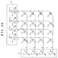
    Figs. 19 to 21 show further another embodiment of the invention. In the embodiment, a construction of a display apparatus is similar to that in the embodiment shown in Figs. 10 and 16 to 18.
    Figs. 19 to 21 show operating states of the B1 scanning period, resetting period, and B2 scanning period in the case where the cathode line B1 is scanned to thereby allow the devices E1,1 and E2,1 to perform the light emission by the control operation of the light emission control circuit 12 and, thereafter, the scan is shifted to the cathode line B2 to thereby allow the devices E2,2 and E3,2 to perform the light emission, respectively. It is assumed that the luminance information obtained from the luminance operating unit 18 at the time shows the dimmer of 50 %. The operating states will now be described.
    First, in Fig. 19, only the scan switch 151 is switched to the ground potential side of 0V and the cathode line B1 is scanned. The inverse bias potential Vcc is applied to the other cathode lines B2 to Bn by the scan switches 152 to 15n. At the same time, the current sources 171 and 172 are connected to the anode lines A1 and A2 by the drive switches 161 and 162. The other anode lines A3 to Am are switched to the ground potential side of 0V by the drive switches 163 to 16m. In the case of Fig. 16, therefore, only the devices E1,1 and E2,1 are biased in the forward direction, the driving current flows from the current sources 171 and 172 as shown by arrows, and only the devices E1,1 and E2,1 perform the light emission. In the light emitting state, each of the non-light emitting devices E3,2 to Em,n shown by hatched capacitor symbols is charged to a polarity as shown in the diagram. The light emitting state is continued only for the driving time of T/2 of the length of the half of the scanning period T.
    When the driving time T/2 elapses from the stationary light emitting state of Fig. 19, the reset control is performed before the scan is shifted to the state where the light emission of the next devices E2,2 and E3,2 is performed. As shown in Fig. 20, the drive switches 162 and 163 are switched so as to apply the bias potential Vcc to the anode lines A2 and A3. The other drive switches 161 and 164 to 16m relay and supply the ground potential to the anode lines A1 and A4 to Am. All of the scan switches 151 to 15n are switched to the inverse bias potential Vcc side. All of the anode lines A2 and A3 and cathode lines B1 to Bn are set to the same potential Vcc. By the reset control, since the voltage across each of the devices E2,1 to E3,n is set to the same electric potential of Vcc, the charges stored in each of the devices E2,1 and E3,2 to E3,n are discharged along routes as shown by arrows in the diagram. The stored charges of those devices are instantaneously extinguished. The electric potential Vcc is applied to the device E1,1 in the backward direction and the device E1,1 is charged to a polarity as shown in the diagram. The charging state of each of the devices E4,2 to Em,n is continued.
    After the resetting period as mentioned above, when the next horizontal scanning period is started, only the scan switch 152 corresponding to the cathode line B2 is now switched to the 0V side as shown in Fig. 21 and the cathode line B2 is scanned. At the same time, the drive switches 162 and 163 are switched to the side of the current sources 172 and 173 and connected to the corresponding anode lines. The other drive switches 161 and 164 to 16m are switched to the ground potential side and 0V is applied to the anode lines A1 and A4 to Am. In the case of Fig. 21, therefore, only the devices E2,2 and E3,2 are biased in the forward direction. The driving current flows from the current sources 172 and 173 as shown by arrows and only the devices E2,2 and E3,2 perform the light emission. In the light emitting state, each of the non-light emitting devices E1,1, E1,3 to E1,n, E4,1 to Em,1, and E4,3 to Em,n shown by hatched capacitor symbols is charged to a polarity as shown in the diagram.
    A length of the B1 scanning period when the scan is shifted from the B1 scanning period of the dimmer of 50 % to the B2 scanning period and a length of the resetting period in the case of using the driving method shown in Figs. 19 to 21 are similar to those shown in Fig. 15. When shifting from the B1 scanning period to the resetting period, the emission of the charges of ne and the charging of the charges of 2e in the device E1,1 occur. In the B2 scanning period, the discharge of the charges of (m-3)e and the charging of the charges of (m+n)e - 3e are similarly performed. now, assuming that m = 4, for easy understanding, a discharge amount of the charges in the B2 scanning period is equal to (n+1)e. That is, a whole amount of charges to be consumed is equal to 2(n+2)e by the operations of Figs. 19 to 21 and an amount of charges to be consumed can be reduced as compared with that in the conventional reset driving method.
    Figs. 22 to 25 show further another embodiment of the invention. In the embodiment, a construction of a display apparatus is similar to that in the embodiment shown in Figs. 10 and 12 to 14.
    Figs. 22 to 25 show operating states of the B1 scanning period, resetting period, and B2 scanning period in the case where the cathode line B1 is scanned to thereby allow the devices E1,1 and E2,1 to perform the light emission by the control operation of the light emission control circuit 12 and, thereafter, the scan is shifted to the cathode line B2 to thereby allow the devices E2,2 and E3,2 to perform the light emission, respectively. It is assumed that the luminance information obtained from the from the luminance operating unit 18 at the time shows the dimmer of 50 % and, further, a gradation ratio of the devices E1,1 and E2,1 is equal to 1 : ½ in the dimmer of 50 %. The operating states will now be described.
    First, in Fig. 22, only the scan switch 151 is switched to the ground potential side of 0V and the cathode line B1 is scanned. The inverse bias potential Vcc is applied to the other cathode lines B2 to Bn by the scan switches 152 to 15n. At the same time, the current sources 171 and 172 are connected to the anode lines A1 and A2 by the drive switches 161 and 162. The other anode lines A3 to Am are switched to the ground potential side of 0V by the drive switches 163 to 16m. In the case of Fig. 22, therefore, only the devices E1,1 and E2,1 are biased in the forward direction, the driving current flows from the current sources 171 and 172 as shown by arrows, and only the devices E1,1 and E2,1 perform the light emission. In the light emitting state, each of the non-light emitting devices E3,2 to Em,n shown by hatched capacitor symbols is charged to a polarity as shown in the diagram.
    When the time of a length of T/4 of the scanning period T elapses from the start of the light emission in Fig. 22, as shown in Fig. 23, the drive switch 162 is switched to the ground potential side and the switching state of the drive switch 161 is maintained. The scan of the cathode line B1 is held. Since the voltage across the device E2,1 is equal to the ground potential, therefore, the charges stored in the device E2,1 are discharged along routes as shown by arrows in the diagram. Since the inverse bias potential Vcc is applied to each of the devices E2,2 to E2,n, each of the devices E2,2 to E2,n is charged to a polarity as shown in the diagram.
    When the light emitting state of Fig. 23 continues only for the time T/4, the reset control is performed. All of the drive switches 161 to 16m and the scan switches 151 to 15n are switched to the ground potential side of 0V as shown in Fig. 24 and all of the anode lines A1 to Am and cathode lines B1 to Bn are set to the same ground potential of 0V. By the reset control, since all of the anode lines and cathode lines are set to the same electric potential of 0V, the charges stored in each device are discharged along routes as shown by arrows in the diagram. The stored charges of all of the devices are instantaneously extinguished.
    After the stored charges of all devices are set to zero as mentioned above, when the next horizontal scanning period is started, only the scan switch 152 corresponding to the cathode line B2 is now switched to the 0V side as shown in Fig. 25 and the cathode line B2 is scanned. At the same time, the drive switches 162 and 163 are switched to the side of the current sources 172 and 173 and connected to the corresponding anode lines. The other drive switches 161 and 164 to 16m are switched to the ground potential side and held and 0V is applied to the anode lines A1 and A4 to Am. In the case of Fig. 25, therefore, only the devices E2,2 and E3,2 are biased in the forward direction. The driving current flows from the current sources 172 and 173 as shown by arrows and only the devices E2,2 and E3,2 perform the light emission. In the light emitting state, each of the non-light emitting devices E1,1, E1,3 to E1,n, E4,3 to Em,1, and E4,3 to Em,n shown by hatched capacitor symbols is charged to a polarity as shown in the diagram.
    In the B1 scanning period of the dimmer of 50 % in the case of using the driving method of Figs. 22 to 25, as shown in Fig. 26, the light emitting operation for scanning the cathode line B1 and allowing the devices E1,1 and E2,1 to perform the light emission is executed only for the former half driving time of T/4, and the light emitting operation for allowing only the device E1,1 to perform the light emission is executed only for the latter half driving time of T/4. A gradation ratio of the devices E1,1 and E2,1 is, thus, equal to 1 : ½. In the next resetting period, as mentioned above, the voltages across all of the devices are set to the same ground potential. The resetting period is continued until the next B2 scanning period is started. In the B2 scanning period, the scan is shifted to the cathode line B2 to thereby allow the devices E2,2 and E3,2 to perform the light emission. In the case, when the operation is shifted to the latter half light emitting operation of only the device E1,1 in the B1 scanning period, the emission of the charges of e and the charging of the charges of (n-1)e occur. When shifting from the B1 scanning period to the resetting period, the emission of the charges of (m-1)(n-1)e + e occurs. In the B2 scanning period, the charging of the charges of [2 + (m-2)(n-1)]e is similarly performed. Now, assuming that m = 4, an emission amount of the charges in the resetting period is equal to (3n-2)e and a charging amount of the charges in the B2 scanning period is equal to 2ne. That is, a whole amount of charges to be consumed is equal to (6n-3)e by the operations of Figs. 22 to 25 and an amount of charges to be consumed can be reduced as compared with that in the conventional reset driving method.
    Although each of the embodiments has been described with respect to the dimmer of 50 %, even in the case of the intermediate luminance in which the percentage of the dimmer is equal to a value other than 50 %, an amount of charges to be consumed can be reduced by the operations similar to those mentioned above.
    The electric potentials which are applied to the driving lines and scanning lines are not limited to the ground potential and bias potential Vcc.
    Further, although the embodiment has been constructed in a manner such that the luminance information is derived from the luminance operating unit 18, the luminance information of every pixel shown by the input image data can be also obtained and used.
    According to the invention as described above, the electric power consumption can be reduced in the case of the gradation display and the intermediate luminance as compared with that in the reset driving method of the conventional simple matrix display panel.

    Claims (7)

    1. A driving method of a display apparatus having a plurality of driving lines, a plurality of scanning lines and a plurality of capacitive light emitting devices connected between said scanning lines and said driving lines at a plurality of crossing positions by said driving lines and said scanning lines. comprising the steps of:
      selecting some of said plurality of driving lines for a scanning period in a predetermined cyclic period consisting of the scanning period and a resetting period subsequent thereto, selecting one of said plurality of scanning lines in order, connecting current sources to the selected driving lines, and supplying a current in the forward direction to each of the capacitive light emitting devices between said selected driving lines and said selected one scanning line; and
      in said resetting period, applying a same electric potential to driving lines to be selected for at least a next scanning period and all of said plurality of scanning lines, thereby discharging charges of the capacitive light emitting devices between the driving lines to be selected and all of the scanning lines,
      wherein a length of the scanning period in said predetermined cyclic period is changed in response to a luminance information command indicative of a display luminance, and the period other than the scanning period in said predetermined cyclic period is set to said resetting period.
    2. A method according to claim 1, wherein in said resetting period, a ground potential is applied to all of said plurality of driving lines and all of said plurality of scanning lines.
    3. A method according to claim 1, wherein in said resetting period, a same electric potential as a specified light emission voltage of said capacitive light emitting device is applied to the selected driving lines for the present scanning period, the driving lines to be selected for the next scanning period and all of said plurality of scanning lines, and a ground potential is applied to the driving lines other than both of the selected driving lines for the present scanning period and the driving lines to be selected for the next scanning period.
    4. A method according to claim 1, wherein in said resetting period, a same electric potential as a specified light emission voltage of said capacitive light emitting device is applied to the selected driving lines for a next scanning period and all of said plurality of scanning lines, and a ground potential is applied to the driving lines other than the driving lines to be selected for said next scanning period.
    5. A method according to claim 1, wherein a length of said scanning period is changed for each of the present selected driving lines, and a period is shifted to said resetting period after the end of a longest one of the different scanning periods.
    6. A method according to claim 1, wherein each of said capacitive light emitting devices is an organic electroluminescence device.
    7. A display apparatus comprising:
      a plurality of driving lines and a plurality of scanning lines;
      a plurality of capacitive light emitting devices connected between said scanning lines and said driving lines at a plurality of crossing positions by said driving lines and said scanning lines;
      scanning period control means for selecting some of said plurality of driving lines in a scanning period in predetermined cyclic period consisting of the scanning period and a resetting period subsequent thereto, selecting one of said plurality of scanning lines in order, connecting current sources to the selected driving lines, and supplying a current in the forward direction to each of the capacitive light emitting devices between said selected driving lines and said selected one scanning line; and
      resetting period control means for applying a same electric potential to driving lines to be selected for at least a next scanning period and all of said plurality of scanning lines in said resetting period, thereby discharging charges of the capacitive light emitting devices between the driving lines to be selected and all of said scanning lines,
      wherein a length of the scanning period in said predetermined cyclic period is changed in response to a luminance information command indicative of a display luminance, and the period other than the scanning period in said predetermined cyclic period is set to said resetting period.
    EP00104392A 1999-03-04 2000-03-02 Display apparatus of capacitive light emitting devices Withdrawn EP1033902A3 (en)

    Applications Claiming Priority (2)

    Application Number Priority Date Filing Date Title
    JP05757199A JP3642463B2 (en) 1999-03-04 1999-03-04 Capacitive light emitting device display device and driving method thereof
    JP5757199 1999-03-04

    Publications (2)

    Publication Number Publication Date
    EP1033902A2 true EP1033902A2 (en) 2000-09-06
    EP1033902A3 EP1033902A3 (en) 2004-08-18

    Family

    ID=13059545

    Family Applications (1)

    Application Number Title Priority Date Filing Date
    EP00104392A Withdrawn EP1033902A3 (en) 1999-03-04 2000-03-02 Display apparatus of capacitive light emitting devices

    Country Status (3)

    Country Link
    US (1) US6552703B1 (en)
    EP (1) EP1033902A3 (en)
    JP (1) JP3642463B2 (en)

    Cited By (2)

    * Cited by examiner, † Cited by third party
    Publication number Priority date Publication date Assignee Title
    EP1253576A2 (en) * 2001-04-25 2002-10-30 Lg Electronics Inc. Method for driving display panel
    EP1471494A1 (en) * 2003-04-24 2004-10-27 Barco N.V. Organic light-emitting diode drive circuit for a display application

    Families Citing this family (19)

    * Cited by examiner, † Cited by third party
    Publication number Priority date Publication date Assignee Title
    JP3737889B2 (en) * 1998-08-21 2006-01-25 パイオニア株式会社 Light emitting display device and driving method
    JP2000298456A (en) * 1999-02-10 2000-10-24 Tdk Corp Display device
    JP3758930B2 (en) * 2000-03-17 2006-03-22 三星エスディアイ株式会社 Image display apparatus and driving method thereof
    JP2002116732A (en) 2000-10-05 2002-04-19 Pioneer Electronic Corp Luminous panel driving method and device
    JP4838431B2 (en) * 2001-01-29 2011-12-14 キヤノン株式会社 Image display device
    JP4123791B2 (en) * 2001-03-05 2008-07-23 富士ゼロックス株式会社 Light emitting element driving apparatus and light emitting element driving system
    JP2003091259A (en) * 2001-09-18 2003-03-28 Tohoku Pioneer Corp Device for driving light-emitting display panel
    JP2003122303A (en) * 2001-10-16 2003-04-25 Matsushita Electric Ind Co Ltd EL display panel, display device using the same, and driving method thereof
    US7071932B2 (en) * 2001-11-20 2006-07-04 Toppoly Optoelectronics Corporation Data voltage current drive amoled pixel circuit
    US7612749B2 (en) * 2003-03-04 2009-11-03 Chi Mei Optoelectronics Corporation Driving circuits for displays
    JP2006003752A (en) * 2004-06-18 2006-01-05 Casio Comput Co Ltd Display device and drive control method thereof
    KR100611660B1 (en) * 2004-12-01 2006-08-10 삼성에스디아이 주식회사 Organic electroluminescent device and operation method
    JP2006215097A (en) * 2005-02-01 2006-08-17 Tohoku Pioneer Corp Unit and method for driving light emitting display panel
    JP4716310B2 (en) * 2005-03-03 2011-07-06 東北パイオニア株式会社 Driving device and driving method of light emitting display panel
    CN100397461C (en) * 2005-06-02 2008-06-25 友达光电股份有限公司 Driving method of display
    WO2008111182A1 (en) * 2007-03-14 2008-09-18 Pioneer Corporation Display and its driving method
    US20100149163A1 (en) * 2008-08-08 2010-06-17 Oqo, Inc. Use of spatial high-pass filtering of images to increase perceived brightness of emissive display
    JP6659968B2 (en) * 2017-03-31 2020-03-04 ミツミ電機株式会社 Battery pack, secondary battery protection integrated circuit, battery monitoring module, and data reading method
    CN113643658B (en) * 2021-10-14 2022-01-14 惠科股份有限公司 Debugging method of display panel, display device and storage medium

    Family Cites Families (10)

    * Cited by examiner, † Cited by third party
    Publication number Priority date Publication date Assignee Title
    JPS53105317A (en) * 1977-02-25 1978-09-13 Hitachi Ltd Luminance adjusting circuit
    EP0106550B1 (en) * 1982-09-21 1989-04-12 Fujitsu Limited Method of driving a matrix type display
    US4652872A (en) * 1983-07-07 1987-03-24 Nec Kansai, Ltd. Matrix display panel driving system
    JPS6289090A (en) * 1985-10-15 1987-04-23 シャープ株式会社 El panel driver
    NL8802436A (en) * 1988-10-05 1990-05-01 Philips Electronics Nv METHOD FOR CONTROLLING A DISPLAY DEVICE
    JP3063453B2 (en) * 1993-04-16 2000-07-12 凸版印刷株式会社 Driving method of organic thin film EL element
    US5594463A (en) * 1993-07-19 1997-01-14 Pioneer Electronic Corporation Driving circuit for display apparatus, and method of driving display apparatus
    JP3507239B2 (en) * 1996-02-26 2004-03-15 パイオニア株式会社 Method and apparatus for driving light emitting element
    JPH10288965A (en) * 1997-04-14 1998-10-27 Casio Comput Co Ltd Display device
    JP2000200067A (en) * 1998-11-06 2000-07-18 Matsushita Electric Ind Co Ltd Display device driving method and display device

    Cited By (4)

    * Cited by examiner, † Cited by third party
    Publication number Priority date Publication date Assignee Title
    EP1253576A2 (en) * 2001-04-25 2002-10-30 Lg Electronics Inc. Method for driving display panel
    US7230590B2 (en) 2001-04-25 2007-06-12 Lg Electronics Inc. Method and apparatus for driving display panel using pulse width modulation
    EP1471494A1 (en) * 2003-04-24 2004-10-27 Barco N.V. Organic light-emitting diode drive circuit for a display application
    US7019721B2 (en) 2003-04-24 2006-03-28 Naamloze Vennootschap, Barco Organic light-emitting diode drive circuit for a display application

    Also Published As

    Publication number Publication date
    JP3642463B2 (en) 2005-04-27
    EP1033902A3 (en) 2004-08-18
    US6552703B1 (en) 2003-04-22
    JP2000259125A (en) 2000-09-22

    Similar Documents

    Publication Publication Date Title
    US6552703B1 (en) Display apparatus of capacitive light emitting devices
    US6965362B1 (en) Apparatus and method for driving light emitting panel
    JP3874390B2 (en) Capacitive light emitting device display device and driving method thereof
    US6707438B1 (en) Apparatus and method for driving multi-color light emitting display panel
    KR100432173B1 (en) Organic EL display device and method for driving the same
    US6774878B2 (en) Drive unit for a luminescence display panel
    JP2002140037A (en) Device and method for driving light emitting panel
    US6369515B1 (en) Display apparatus with capacitive light-emitting devices and method of driving the same
    JP3620985B2 (en) Capacitive light emitting device display device and driving method thereof
    JP3618064B2 (en) Driving device and driving method of light emitting display panel
    US6229267B1 (en) Display apparatus with capacitive light-emitting devices and method of driving the same
    JP4298906B2 (en) Driving device and method for light emitting panel
    JP3609300B2 (en) Driving device for light emitting display panel
    JP2002091378A (en) Method and device for driving capacitive light emitting display panel
    JP3646917B2 (en) Multicolor light emitting display panel drive device
    JP3638830B2 (en) Driving device for light emitting display panel
    JP3646916B2 (en) Multicolor light emitting display panel drive device
    JP3609299B2 (en) Driving device for light emitting display panel
    JP2003043996A (en) Driving device for capacitive light emitting element display panel
    JP2000122609A (en) Capacitive light emitting element display device and driving method therefor
    JP3587355B2 (en) Light emitting display device and driving method thereof
    JP5200313B2 (en) Organic EL display device and driving method thereof
    JP2000112433A (en) Capacitive light emitting element display device and driving method therefor
    KR100498283B1 (en) Structure for matrix of mim fed
    JP2004086051A (en) Matrix drive display device

    Legal Events

    Date Code Title Description
    PUAI Public reference made under article 153(3) epc to a published international application that has entered the european phase

    Free format text: ORIGINAL CODE: 0009012

    AK Designated contracting states

    Kind code of ref document: A2

    Designated state(s): AT BE CH CY DE DK ES FI FR GB GR IE IT LI LU MC NL PT SE

    AX Request for extension of the european patent

    Free format text: AL;LT;LV;MK;RO;SI

    RIC1 Information provided on ipc code assigned before grant

    Ipc: 7G 09G 3/32 B

    Ipc: 7H 05B 33/08 A

    PUAL Search report despatched

    Free format text: ORIGINAL CODE: 0009013

    AK Designated contracting states

    Kind code of ref document: A3

    Designated state(s): AT BE CH CY DE DK ES FI FR GB GR IE IT LI LU MC NL PT SE

    AX Request for extension of the european patent

    Extension state: AL LT LV MK RO SI

    17P Request for examination filed

    Effective date: 20050211

    AKX Designation fees paid

    Designated state(s): DE FR GB

    RBV Designated contracting states (corrected)

    Designated state(s): DE FR GB

    17Q First examination report despatched

    Effective date: 20070808

    STAA Information on the status of an ep patent application or granted ep patent

    Free format text: STATUS: THE APPLICATION IS DEEMED TO BE WITHDRAWN

    18D Application deemed to be withdrawn

    Effective date: 20071219