EP1253576A2 - Method for driving display panel - Google Patents
Method for driving display panel Download PDFInfo
- Publication number
- EP1253576A2 EP1253576A2 EP02009147A EP02009147A EP1253576A2 EP 1253576 A2 EP1253576 A2 EP 1253576A2 EP 02009147 A EP02009147 A EP 02009147A EP 02009147 A EP02009147 A EP 02009147A EP 1253576 A2 EP1253576 A2 EP 1253576A2
- Authority
- EP
- European Patent Office
- Prior art keywords
- pulse width
- signals
- driving
- scan
- data line
- Prior art date
- Legal status (The legal status is an assumption and is not a legal conclusion. Google has not performed a legal analysis and makes no representation as to the accuracy of the status listed.)
- Ceased
Links
Images

Classifications
-
- G—PHYSICS
- G09—EDUCATION; CRYPTOGRAPHY; DISPLAY; ADVERTISING; SEALS
- G09G—ARRANGEMENTS OR CIRCUITS FOR CONTROL OF INDICATING DEVICES USING STATIC MEANS TO PRESENT VARIABLE INFORMATION
- G09G3/00—Control arrangements or circuits, of interest only in connection with visual indicators other than cathode-ray tubes
- G09G3/20—Control arrangements or circuits, of interest only in connection with visual indicators other than cathode-ray tubes for presentation of an assembly of a number of characters, e.g. a page, by composing the assembly by combination of individual elements arranged in a matrix no fixed position being assigned to or needed to be assigned to the individual characters or partial characters
- G09G3/22—Control arrangements or circuits, of interest only in connection with visual indicators other than cathode-ray tubes for presentation of an assembly of a number of characters, e.g. a page, by composing the assembly by combination of individual elements arranged in a matrix no fixed position being assigned to or needed to be assigned to the individual characters or partial characters using controlled light sources
- G09G3/30—Control arrangements or circuits, of interest only in connection with visual indicators other than cathode-ray tubes for presentation of an assembly of a number of characters, e.g. a page, by composing the assembly by combination of individual elements arranged in a matrix no fixed position being assigned to or needed to be assigned to the individual characters or partial characters using controlled light sources using electroluminescent panels
- G09G3/32—Control arrangements or circuits, of interest only in connection with visual indicators other than cathode-ray tubes for presentation of an assembly of a number of characters, e.g. a page, by composing the assembly by combination of individual elements arranged in a matrix no fixed position being assigned to or needed to be assigned to the individual characters or partial characters using controlled light sources using electroluminescent panels semiconductive, e.g. using light-emitting diodes [LED]
- G09G3/3208—Control arrangements or circuits, of interest only in connection with visual indicators other than cathode-ray tubes for presentation of an assembly of a number of characters, e.g. a page, by composing the assembly by combination of individual elements arranged in a matrix no fixed position being assigned to or needed to be assigned to the individual characters or partial characters using controlled light sources using electroluminescent panels semiconductive, e.g. using light-emitting diodes [LED] organic, e.g. using organic light-emitting diodes [OLED]
-
- G—PHYSICS
- G09—EDUCATION; CRYPTOGRAPHY; DISPLAY; ADVERTISING; SEALS
- G09G—ARRANGEMENTS OR CIRCUITS FOR CONTROL OF INDICATING DEVICES USING STATIC MEANS TO PRESENT VARIABLE INFORMATION
- G09G2300/00—Aspects of the constitution of display devices
- G09G2300/06—Passive matrix structure, i.e. with direct application of both column and row voltages to the light emitting or modulating elements, other than LCD or OLED
-
- G—PHYSICS
- G09—EDUCATION; CRYPTOGRAPHY; DISPLAY; ADVERTISING; SEALS
- G09G—ARRANGEMENTS OR CIRCUITS FOR CONTROL OF INDICATING DEVICES USING STATIC MEANS TO PRESENT VARIABLE INFORMATION
- G09G2310/00—Command of the display device
- G09G2310/06—Details of flat display driving waveforms
- G09G2310/066—Waveforms comprising a gently increasing or decreasing portion, e.g. ramp
-
- G—PHYSICS
- G09—EDUCATION; CRYPTOGRAPHY; DISPLAY; ADVERTISING; SEALS
- G09G—ARRANGEMENTS OR CIRCUITS FOR CONTROL OF INDICATING DEVICES USING STATIC MEANS TO PRESENT VARIABLE INFORMATION
- G09G2320/00—Control of display operating conditions
- G09G2320/02—Improving the quality of display appearance
- G09G2320/0209—Crosstalk reduction, i.e. to reduce direct or indirect influences of signals directed to a certain pixel of the displayed image on other pixels of said image, inclusive of influences affecting pixels in different frames or fields or sub-images which constitute a same image, e.g. left and right images of a stereoscopic display
-
- G—PHYSICS
- G09—EDUCATION; CRYPTOGRAPHY; DISPLAY; ADVERTISING; SEALS
- G09G—ARRANGEMENTS OR CIRCUITS FOR CONTROL OF INDICATING DEVICES USING STATIC MEANS TO PRESENT VARIABLE INFORMATION
- G09G3/00—Control arrangements or circuits, of interest only in connection with visual indicators other than cathode-ray tubes
- G09G3/04—Control arrangements or circuits, of interest only in connection with visual indicators other than cathode-ray tubes for presentation of a single character by selection from a plurality of characters, or by composing the character by combination of individual elements, e.g. segments using a combination of such display devices for composing words, rows or the like, in a frame with fixed character positions
- G09G3/06—Control arrangements or circuits, of interest only in connection with visual indicators other than cathode-ray tubes for presentation of a single character by selection from a plurality of characters, or by composing the character by combination of individual elements, e.g. segments using a combination of such display devices for composing words, rows or the like, in a frame with fixed character positions using controlled light sources
- G09G3/12—Control arrangements or circuits, of interest only in connection with visual indicators other than cathode-ray tubes for presentation of a single character by selection from a plurality of characters, or by composing the character by combination of individual elements, e.g. segments using a combination of such display devices for composing words, rows or the like, in a frame with fixed character positions using controlled light sources using electroluminescent elements
- G09G3/14—Semiconductor devices, e.g. diodes
-
- G—PHYSICS
- G09—EDUCATION; CRYPTOGRAPHY; DISPLAY; ADVERTISING; SEALS
- G09G—ARRANGEMENTS OR CIRCUITS FOR CONTROL OF INDICATING DEVICES USING STATIC MEANS TO PRESENT VARIABLE INFORMATION
- G09G3/00—Control arrangements or circuits, of interest only in connection with visual indicators other than cathode-ray tubes
- G09G3/20—Control arrangements or circuits, of interest only in connection with visual indicators other than cathode-ray tubes for presentation of an assembly of a number of characters, e.g. a page, by composing the assembly by combination of individual elements arranged in a matrix no fixed position being assigned to or needed to be assigned to the individual characters or partial characters
- G09G3/2007—Display of intermediate tones
- G09G3/2014—Display of intermediate tones by modulation of the duration of a single pulse during which the logic level remains constant
-
- G—PHYSICS
- G09—EDUCATION; CRYPTOGRAPHY; DISPLAY; ADVERTISING; SEALS
- G09G—ARRANGEMENTS OR CIRCUITS FOR CONTROL OF INDICATING DEVICES USING STATIC MEANS TO PRESENT VARIABLE INFORMATION
- G09G3/00—Control arrangements or circuits, of interest only in connection with visual indicators other than cathode-ray tubes
- G09G3/20—Control arrangements or circuits, of interest only in connection with visual indicators other than cathode-ray tubes for presentation of an assembly of a number of characters, e.g. a page, by composing the assembly by combination of individual elements arranged in a matrix no fixed position being assigned to or needed to be assigned to the individual characters or partial characters
- G09G3/22—Control arrangements or circuits, of interest only in connection with visual indicators other than cathode-ray tubes for presentation of an assembly of a number of characters, e.g. a page, by composing the assembly by combination of individual elements arranged in a matrix no fixed position being assigned to or needed to be assigned to the individual characters or partial characters using controlled light sources
- G09G3/30—Control arrangements or circuits, of interest only in connection with visual indicators other than cathode-ray tubes for presentation of an assembly of a number of characters, e.g. a page, by composing the assembly by combination of individual elements arranged in a matrix no fixed position being assigned to or needed to be assigned to the individual characters or partial characters using controlled light sources using electroluminescent panels
- G09G3/32—Control arrangements or circuits, of interest only in connection with visual indicators other than cathode-ray tubes for presentation of an assembly of a number of characters, e.g. a page, by composing the assembly by combination of individual elements arranged in a matrix no fixed position being assigned to or needed to be assigned to the individual characters or partial characters using controlled light sources using electroluminescent panels semiconductive, e.g. using light-emitting diodes [LED]
- G09G3/3208—Control arrangements or circuits, of interest only in connection with visual indicators other than cathode-ray tubes for presentation of an assembly of a number of characters, e.g. a page, by composing the assembly by combination of individual elements arranged in a matrix no fixed position being assigned to or needed to be assigned to the individual characters or partial characters using controlled light sources using electroluminescent panels semiconductive, e.g. using light-emitting diodes [LED] organic, e.g. using organic light-emitting diodes [OLED]
- G09G3/3216—Control arrangements or circuits, of interest only in connection with visual indicators other than cathode-ray tubes for presentation of an assembly of a number of characters, e.g. a page, by composing the assembly by combination of individual elements arranged in a matrix no fixed position being assigned to or needed to be assigned to the individual characters or partial characters using controlled light sources using electroluminescent panels semiconductive, e.g. using light-emitting diodes [LED] organic, e.g. using organic light-emitting diodes [OLED] using a passive matrix
-
- G—PHYSICS
- G09—EDUCATION; CRYPTOGRAPHY; DISPLAY; ADVERTISING; SEALS
- G09G—ARRANGEMENTS OR CIRCUITS FOR CONTROL OF INDICATING DEVICES USING STATIC MEANS TO PRESENT VARIABLE INFORMATION
- G09G3/00—Control arrangements or circuits, of interest only in connection with visual indicators other than cathode-ray tubes
- G09G3/20—Control arrangements or circuits, of interest only in connection with visual indicators other than cathode-ray tubes for presentation of an assembly of a number of characters, e.g. a page, by composing the assembly by combination of individual elements arranged in a matrix no fixed position being assigned to or needed to be assigned to the individual characters or partial characters
- G09G3/22—Control arrangements or circuits, of interest only in connection with visual indicators other than cathode-ray tubes for presentation of an assembly of a number of characters, e.g. a page, by composing the assembly by combination of individual elements arranged in a matrix no fixed position being assigned to or needed to be assigned to the individual characters or partial characters using controlled light sources
- G09G3/30—Control arrangements or circuits, of interest only in connection with visual indicators other than cathode-ray tubes for presentation of an assembly of a number of characters, e.g. a page, by composing the assembly by combination of individual elements arranged in a matrix no fixed position being assigned to or needed to be assigned to the individual characters or partial characters using controlled light sources using electroluminescent panels
- G09G3/32—Control arrangements or circuits, of interest only in connection with visual indicators other than cathode-ray tubes for presentation of an assembly of a number of characters, e.g. a page, by composing the assembly by combination of individual elements arranged in a matrix no fixed position being assigned to or needed to be assigned to the individual characters or partial characters using controlled light sources using electroluminescent panels semiconductive, e.g. using light-emitting diodes [LED]
- G09G3/3208—Control arrangements or circuits, of interest only in connection with visual indicators other than cathode-ray tubes for presentation of an assembly of a number of characters, e.g. a page, by composing the assembly by combination of individual elements arranged in a matrix no fixed position being assigned to or needed to be assigned to the individual characters or partial characters using controlled light sources using electroluminescent panels semiconductive, e.g. using light-emitting diodes [LED] organic, e.g. using organic light-emitting diodes [OLED]
- G09G3/3275—Details of drivers for data electrodes
Abstract
Description
- This application claims the benefit of the Korean Application No. P2001-22283 filed on April 25, 2001, which is hereby incorporated by reference.
- The present invention relates to a display device, and more particularly, to a method for driving a display panel to form a desired waveform in driving a pulse width modulation (PWM) mode for adjusting a gray scale level.
- Generally, a gray scale level in a display device means an achromatic color system corresponding to colors from white to black.
- To digitally drive such a gray scale, a PWM driving method is widely used. The PWM driving method is used for almost display devices regardless of passive driving or active driving.
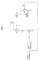
- FIG. 1 shows a circuit for adjusting a gray scale level of an organic electroluminescent (EL) panel according to the related art. As shown in FIG. 1, a PWM controller is added to a segment driving part of the organic EL panel.
- The PWM controller added to the segment driving part is controlled in accordance with a segment signal, so that a pulse width of a signal applied to the display device is adjusted, thereby setting a gray scale level.
- However, in such a PWM driving method, since a start time on all data lines of a data segment is fixed, a problem may occur in case of an organic EL panel.
- Such a problem will be described with reference to the accompanying drawings.
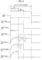
- FIG. 2 shows a PWM driving waveform of a related art display panel.
- Referring to FIG. 2, the PWM driving method according to the related art is performed in such a manner that all signals are simultaneously turned on for one scan pulse width Ts and when a desired pulse width is obtained, a data line signal is shorted to turn off pixels.
- Such a PWM driving method results in distortion of the waveform due to fluctuation of a voltage in an anode line in case of an organic EL panel.
- In other words, on data line of a data segment of FIG. 1, a signal type of a first data line corresponds to a data line signal turned on within one scan pulse width, a signal type of a second data line corresponds to a data line signal turned on for a time period T2 only, and a signal type of a third data line corresponds to a data line signal turned on for a time period T1 only.
- A signal waveform of an anode line applied to the panel through a driver shown in FIG. 1 is the same as signal waveforms of first, second and third anode lines.
- In other words, since there is no signal waveform shorter than a signal waveform of the third anode line, the signal waveform of the third anode line occurs normally. However, a wave distortion A occurs in a signal waveform of the second anode line due to the signal waveform of the third anode line. Two wave distortions B and C occur in a signal waveform of the first anode line due to the signal waveforms of the second and third anode lines.
- The wave distortions give an adverse effect to longevity of the display device due to luminance and momentary high voltage.
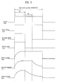
- To solve such a problem, a PWM driving waveform as shown in FIG. 3 has been supposed.
- Referring to FIG. 3, if no signal is input from the data line of the data segment to the display device, the display device floats the anode line to naturally consume charges inside the organic EL panel.
- Momentary change in the signal waveform of the anode line is relieved as the charges inside the organic EL panel are naturally consumed. As shown in FIG. 3, it is noted that distortion of the signal waveform on the anode line is reduced.
- However, the PWM driving method of FIG. 3 has a problem in that it is difficult to exactly adjust a gray level due to waveform of the PWM. Also, charges trapped inside pixels give an adverse effect to longevity of the display panel.
- Accordingly, the present invention is directed to a method for driving a display panel that substantially obviates one or more problems due to limitations and disadvantages of the related art.
- An object of the present invention is to provide a method for driving a display panel that is not affected by an anode line and exactly adjusts a gray scale.
- Additional advantages, objects, and features of the invention will be set forth in part in the description which follows and in part will become apparent to those having ordinary skill in the art upon examination of the following or may be learned from practice of the invention. The objectives and other advantages of the invention may be realized and attained by the structure particularly pointed out in the written description and claims hereof as well as the appended drawings.
- To achieve these objects and other advantages and in accordance with the purpose of the invention, as embodied and broadly described herein, a method for driving a display panel includes the steps of previously turning off a plurality of signals respectively applied from a data line and/or a scan line based on a falling edge of one scan pulse, and next transiting the signals to a turn-on state to have a predetermined pulse width, thereby adjusting a gray level of the signals using a pulse width modulation mode.
- Preferably, the signals are turned off from a time period of a falling edge of one scan pulse within one scan pulse width and then turned on from a time period of a difference between one scan pulse width and a predetermined pulse width of each signal.
- In another aspect of the present invention, a method for driving an organic EL panel includes the steps of turning off a plurality of signals respectively applied from a data line and/or a scan line based on a falling edge of one scan pulse, and transiting the signals to a turn-on state to have a predetermined pulse width, thereby adjusting a gray level of the signals using a pulse width modulation mode.
- Preferably, the signals are turned off from a time period of a falling edge of one scan pulse within one scan pulse width and then turned on from a time period of a difference between one scan pulse width and a predetermined pulse width of each signal.
- In other aspect of the present invention, a method for driving a display panel includes the steps of fixing a turn-off time period of a plurality of signals applied from a data line and/or a scan line based on a falling edge of one scan pulse and transiting the signals to a turn-on state to have a predetermined pulse width based on the fixed turn-off time period, thereby adjusting a gray level of the signals using a pulse width modulation mode.
- It is to be understood that both the foregoing general description and the following detailed description of the present invention are exemplary and explanatory and are intended to provide further explanation of the invention as claimed.
- The accompanying drawings, which are included to provide a further understanding of the invention and are incorporated in and constitute a part of this application, illustrate embodiment(s) of the invention and together with the description serve to explain the principle of the invention. In the drawings:
- FIG. 1 illustrates a circuit for adjusting a gray scale level of an organic EL panel according to the related art;
- FIG. 2 illustrates a PWM driving waveform of a related art display panel;
- FIG. 3 illustrates an improved PWM driving waveform of a related art display panel; and
- FIG. 4 illustrates a PWM driving waveform of a display panel according to the present invention.
- Reference will now be made in detail to the preferred embodiments of the present invention, examples of which are illustrated in the accompanying drawings. Wherever possible, the same reference numbers will be used throughout the drawings to refer to the same or like parts.
- A method for driving a display panel according to the present invention will be described with reference to the accompanying drawings.
- FIG. 4 illustrates a PWM driving waveform of a display panel according to the present invention.
- Referring to FIG. 4, a plurality of data signals applied from a data line of a data segment are turned on for a pulse width adjusted by PWM based on a falling edge of one scan pulse, so that a gray level is adjusted. At this time, a turn-off time period of signal waveforms applied from all the data lines based on the falling edge of one scan pulse is fixed. Afterwards, the signal waveforms are turned on to maintain the adjusted pulse width.
- If data having a long pulse width that turns on the data line is applied, the pulse width of the turned-off data line becomes short and the pulse width of the turned-on data line becomes longer. However, the whole scan pulse width is maintained unchanged.
- As an example, on the data line of the data segment, a signal waveform of a first data line corresponds to a data line signal turned on within one scan pulse width, a signal waveform of a second data line corresponds to a data line signal turned on for a time period T2 only, and a signal waveform of a third data line corresponds to a data line signal turned on for a time period T1 only.
- The signal waveform of the anode line applied to the panel through the driver shown in FIG. 1 is the same as the waveforms of the first, second and third anode lines.
- In other words, signal waveforms of the first anode line and the first data line are turned on for a time period of Ts, while the signal waveforms of the second anode line and the second data line are turned off for a time period of Ts-T2 and turned on for a time period of T2. The signal waveforms of the third anode line and the third data line are turned off for a time period of Ts-T1 and turned on for a time period of T1.
- The signal waveforms of the first to third anode lines have a slope period for a predetermined time from the time when they are turned on.
- As described above, in the present invention, at least one data line and at least one anode line based on a falling edge of one scan pulse are initially turned off. To maintain turn-on time by the predetermined pulse width, the data line and the anode line are transited to turn-on state at a corresponding time period. Therefore, momentary change in waveforms can be relieved and a gray level can exactly be adjusted.
- Since one scan pulse width is in advance defined, the pulse width applied to the data line and the anode line can simply be adjusted based on a falling edge of one scan pulse.
- As aforementioned, the method for driving a display panel according to the present invention has the following advantages.
- First, it is possible to provide a method for generating an exact gray scale. Second, it is possible to provide a clear driving signal waveform having no distortion. Third, no overvoltage is applied to pixels even in case of signals having different pulse widths. Consequently, it is possible to provide a good effect to longevity of the organic EL panel.
- It will be apparent to those skilled in the art that various modifications and variations can be made in the present invention. Thus, it is intended that the present invention covers the modifications and variations of this invention provided they come within the scope of the appended claims and their equivalents.
Claims (5)
- A-method for driving a display panel comprising the steps of:turning off a plurality of signals respectively applied from a data line and/or a scan line based on a falling edge of one scan pulse; andtransiting the signals to a turn-on state to have a predetermined pulse width, thereby adjusting a gray level of the signals using a pulse width modulation mode.
- The method of claim 1, wherein the signals are turned off from a time period of a falling edge of one scan pulse within one scan pulse width and then turned on from a time period of a difference between one scan pulse width and a predetermined pulse width of each signal.
- A method for driving an organic EL panel comprising the steps of:turning off a plurality of signals respectively applied from a data line and/or a scan line based on a falling edge of one scan pulse; andtransiting the signals to a turn-on state to have a predetermined pulse width, thereby adjusting a gray level of the signals using a pulse width modulation mode.
- The method of claim 3, wherein the signals are turned off from a time period of a falling edge of one scan pulse within one scan pulse width and then turned on from a time period of a difference between one scan pulse width and a predetermined pulse width of each signal.
- A method for driving a display panel comprising the steps of:fixing a turn-off time period of a plurality of signals applied from a data line and/or a scan line based on a falling edge of one scan pulse; andtransiting the signals to a turn-on state to have a predetermined pulse width based on the fixed turn-off time period, thereby adjusting a gray level of the signals using a pulse width modulation mode.
Applications Claiming Priority (2)
| Application Number | Priority Date | Filing Date | Title |
|---|---|---|---|
| KR2001022283 | 2001-04-25 | ||
| KR10-2001-0022283A KR100413437B1 (en) | 2001-04-25 | 2001-04-25 | method for driving control in display panel |
Publications (2)
| Publication Number | Publication Date |
|---|---|
| EP1253576A2 true EP1253576A2 (en) | 2002-10-30 |
| EP1253576A3 EP1253576A3 (en) | 2003-02-26 |
Family
ID=19708682
Family Applications (1)
| Application Number | Title | Priority Date | Filing Date |
|---|---|---|---|
| EP02009147A Ceased EP1253576A3 (en) | 2001-04-25 | 2002-04-24 | Method for driving display panel |
Country Status (4)
| Country | Link |
|---|---|
| US (1) | US7230590B2 (en) |
| EP (1) | EP1253576A3 (en) |
| KR (1) | KR100413437B1 (en) |
| CN (1) | CN1197042C (en) |
Cited By (2)
| Publication number | Priority date | Publication date | Assignee | Title |
|---|---|---|---|---|
| WO2004077394A1 (en) * | 2003-02-28 | 2004-09-10 | Koninklijke Philips Electronics N.V. | Driving a matrix display |
| JP2005078096A (en) * | 2003-09-02 | 2005-03-24 | Samsung Electronics Co Ltd | Method and device for driving data lines, and display device having the same |
Families Citing this family (5)
| Publication number | Priority date | Publication date | Assignee | Title |
|---|---|---|---|---|
| JP4662011B2 (en) * | 2003-07-29 | 2011-03-30 | 東北パイオニア株式会社 | Driving device and driving method of light emitting display panel |
| KR100927608B1 (en) * | 2003-10-09 | 2009-11-23 | 삼성에스디아이 주식회사 | A luminance control method and apparatus in an image display apparatus |
| KR100921506B1 (en) * | 2007-04-24 | 2009-10-13 | 한양대학교 산학협력단 | Display and method of driving the same |
| KR100897139B1 (en) * | 2007-08-08 | 2009-05-14 | 삼성에스디아이 주식회사 | Electron emission device for back light unit and liquid crystal display thereof |
| CN112102740B (en) * | 2020-09-29 | 2022-05-03 | 厦门天马微电子有限公司 | Display panel, driving method thereof and display device |
Citations (4)
| Publication number | Priority date | Publication date | Assignee | Title |
|---|---|---|---|---|
| EP0372364A1 (en) * | 1988-11-30 | 1990-06-13 | Sharp Kabushiki Kaisha | Method and apparatus for driving display device |
| US6023259A (en) * | 1997-07-11 | 2000-02-08 | Fed Corporation | OLED active matrix using a single transistor current mode pixel design |
| EP1033902A2 (en) * | 1999-03-04 | 2000-09-06 | Pioneer Corporation | Display apparatus of capacitive light emitting devices |
| JP2000310968A (en) * | 1999-02-23 | 2000-11-07 | Canon Inc | Device and method for picture display |
Family Cites Families (11)
| Publication number | Priority date | Publication date | Assignee | Title |
|---|---|---|---|---|
| JPH0748143B2 (en) | 1988-12-28 | 1995-05-24 | シャープ株式会社 | Driving method of display device |
| JP2628766B2 (en) | 1989-11-15 | 1997-07-09 | シャープ株式会社 | Driving method of thin film EL display device |
| US5999150A (en) * | 1996-04-17 | 1999-12-07 | Northrop Grumman Corporation | Electroluminescent display having reversible voltage polarity |
| US5789870A (en) * | 1996-05-06 | 1998-08-04 | Durel Corporation | Low noise inverter for EL lamp |
| US6310589B1 (en) * | 1997-05-29 | 2001-10-30 | Nec Corporation | Driving circuit for organic thin film EL elements |
| JP3102411B2 (en) | 1997-05-29 | 2000-10-23 | 日本電気株式会社 | Driving circuit for organic thin film EL device |
| US6038153A (en) * | 1997-06-09 | 2000-03-14 | Telefonaktiebolaget Lm Ericsson | Inverter circuit for illuminating an electroluminescent lamp |
| JP2000020019A (en) * | 1998-06-30 | 2000-01-21 | Toshiba Corp | Field emission display device |
| TW420967B (en) * | 1998-11-27 | 2001-02-01 | Sanyo Electric Co | Electroluminescence display device |
| US6198226B1 (en) * | 1999-08-18 | 2001-03-06 | Astronics Corporation | Low-noise drive circuit for electroluminescent lamp, and electroluminescent lamp assembly comprising same |
| US6507156B2 (en) * | 2000-05-16 | 2003-01-14 | Planar Systems, Inc. | Display |
-
2001
- 2001-04-25 KR KR10-2001-0022283A patent/KR100413437B1/en not_active IP Right Cessation
-
2002
- 2002-04-22 US US10/126,547 patent/US7230590B2/en not_active Expired - Lifetime
- 2002-04-24 EP EP02009147A patent/EP1253576A3/en not_active Ceased
- 2002-04-25 CN CNB02121848XA patent/CN1197042C/en not_active Expired - Fee Related
Patent Citations (4)
| Publication number | Priority date | Publication date | Assignee | Title |
|---|---|---|---|---|
| EP0372364A1 (en) * | 1988-11-30 | 1990-06-13 | Sharp Kabushiki Kaisha | Method and apparatus for driving display device |
| US6023259A (en) * | 1997-07-11 | 2000-02-08 | Fed Corporation | OLED active matrix using a single transistor current mode pixel design |
| JP2000310968A (en) * | 1999-02-23 | 2000-11-07 | Canon Inc | Device and method for picture display |
| EP1033902A2 (en) * | 1999-03-04 | 2000-09-06 | Pioneer Corporation | Display apparatus of capacitive light emitting devices |
Cited By (2)
| Publication number | Priority date | Publication date | Assignee | Title |
|---|---|---|---|---|
| WO2004077394A1 (en) * | 2003-02-28 | 2004-09-10 | Koninklijke Philips Electronics N.V. | Driving a matrix display |
| JP2005078096A (en) * | 2003-09-02 | 2005-03-24 | Samsung Electronics Co Ltd | Method and device for driving data lines, and display device having the same |
Also Published As
| Publication number | Publication date |
|---|---|
| US20020158892A1 (en) | 2002-10-31 |
| EP1253576A3 (en) | 2003-02-26 |
| CN1197042C (en) | 2005-04-13 |
| CN1383122A (en) | 2002-12-04 |
| KR100413437B1 (en) | 2003-12-31 |
| US7230590B2 (en) | 2007-06-12 |
| KR20020083024A (en) | 2002-11-01 |
Similar Documents
| Publication | Publication Date | Title |
|---|---|---|
| US7233302B2 (en) | Display apparatus with active matrix type display panel | |
| US5973456A (en) | Electroluminescent display device having uniform display element column luminosity | |
| US6034659A (en) | Active matrix electroluminescent grey scale display | |
| US7119773B2 (en) | Apparatus and method for controlling gray level for display panel | |
| KR102496782B1 (en) | Voltage conversion circuit and organic lighting emitting device having the saeme | |
| JP4406372B2 (en) | Display device and control method thereof | |
| KR101025525B1 (en) | Device and method for varying the row scanning time to compensate the signal attenuation depending on the distance between pixel rows and column driver | |
| EP1253576A2 (en) | Method for driving display panel | |
| US6509690B2 (en) | Display device | |
| JP2000284750A (en) | Display device | |
| US20100259526A1 (en) | Scanning circuit, scanning device, image display apparatus and television apparatus | |
| KR20050037303A (en) | Method for driving electro-luminescence display panel wherein preliminary charging is selectively performed | |
| US6407727B1 (en) | Display device | |
| CN100539781C (en) | Light-emitting device and driving method thereof | |
| US10163398B2 (en) | Method of driving a display panel and a display apparatus for performing the same | |
| KR20070100621A (en) | Method for driving display | |
| US8519991B2 (en) | Image display apparatus and control method thereof for controlling brightness unevenness due to resistance of column wirings | |
| KR100955377B1 (en) | Driving method of liquid crystal display panel | |
| KR100634752B1 (en) | drive method of organic elecroluminescence display device | |
| KR20050112769A (en) | Driving method of electron emission device with decreased signal distortion and device implementing thereof | |
| JPH05206550A (en) | Light emitting element drive circuit | |
| US10909932B2 (en) | Display apparatus and method of driving display panel using the same | |
| CN117037703A (en) | Display panel and display device | |
| EP1833039A1 (en) | Flat display unit and displaying drive method | |
| JPS60216388A (en) | El driver |
Legal Events
| Date | Code | Title | Description |
|---|---|---|---|
| PUAI | Public reference made under article 153(3) epc to a published international application that has entered the european phase |
Free format text: ORIGINAL CODE: 0009012 |
|
| AK | Designated contracting states |
Kind code of ref document: A2 Designated state(s): AT BE CH CY DE DK ES FI FR GB GR IE IT LI LU MC NL PT SE TR |
|
| AX | Request for extension of the european patent |
Free format text: AL;LT;LV;MK;RO;SI |
|
| PUAL | Search report despatched |
Free format text: ORIGINAL CODE: 0009013 |
|
| AK | Designated contracting states |
Kind code of ref document: A3 Designated state(s): AT BE CH CY DE DK ES FI FR GB GR IE IT LI LU MC NL PT SE TR Designated state(s): AT BE CH CY DE DK ES FI FR GB GR IE IT LI LU MC NL PT SE TR |
|
| AX | Request for extension of the european patent |
Extension state: AL LT LV MK RO SI |
|
| 17P | Request for examination filed |
Effective date: 20030731 |
|
| 17Q | First examination report despatched |
Effective date: 20030902 |
|
| AKX | Designation fees paid |
Designated state(s): DE FR GB NL |
|
| STAA | Information on the status of an ep patent application or granted ep patent |
Free format text: STATUS: THE APPLICATION HAS BEEN REFUSED |
|
| 18R | Application refused |
Effective date: 20051024 |