EP1033760A2 - High withstand voltage MOS transistor and method of producing the same - Google Patents
High withstand voltage MOS transistor and method of producing the same Download PDFInfo
- Publication number
- EP1033760A2 EP1033760A2 EP00103907A EP00103907A EP1033760A2 EP 1033760 A2 EP1033760 A2 EP 1033760A2 EP 00103907 A EP00103907 A EP 00103907A EP 00103907 A EP00103907 A EP 00103907A EP 1033760 A2 EP1033760 A2 EP 1033760A2
- Authority
- EP
- European Patent Office
- Prior art keywords
- conductivity type
- layer
- type
- region
- semiconductor device
- Prior art date
- Legal status (The legal status is an assumption and is not a legal conclusion. Google has not performed a legal analysis and makes no representation as to the accuracy of the status listed.)
- Withdrawn
Links
Images





Classifications
-
- H—ELECTRICITY
- H10—SEMICONDUCTOR DEVICES; ELECTRIC SOLID-STATE DEVICES NOT OTHERWISE PROVIDED FOR
- H10D—INORGANIC ELECTRIC SEMICONDUCTOR DEVICES
- H10D30/00—Field-effect transistors [FET]
- H10D30/60—Insulated-gate field-effect transistors [IGFET]
- H10D30/64—Double-diffused metal-oxide semiconductor [DMOS] FETs
- H10D30/65—Lateral DMOS [LDMOS] FETs
-
- H—ELECTRICITY
- H10—SEMICONDUCTOR DEVICES; ELECTRIC SOLID-STATE DEVICES NOT OTHERWISE PROVIDED FOR
- H10D—INORGANIC ELECTRIC SEMICONDUCTOR DEVICES
- H10D30/00—Field-effect transistors [FET]
- H10D30/01—Manufacture or treatment
- H10D30/021—Manufacture or treatment of FETs having insulated gates [IGFET]
- H10D30/028—Manufacture or treatment of FETs having insulated gates [IGFET] of double-diffused metal oxide semiconductor [DMOS] FETs
- H10D30/0281—Manufacture or treatment of FETs having insulated gates [IGFET] of double-diffused metal oxide semiconductor [DMOS] FETs of lateral DMOS [LDMOS] FETs
-
- H—ELECTRICITY
- H10—SEMICONDUCTOR DEVICES; ELECTRIC SOLID-STATE DEVICES NOT OTHERWISE PROVIDED FOR
- H10D—INORGANIC ELECTRIC SEMICONDUCTOR DEVICES
- H10D62/00—Semiconductor bodies, or regions thereof, of devices having potential barriers
- H10D62/10—Shapes, relative sizes or dispositions of the regions of the semiconductor bodies; Shapes of the semiconductor bodies
- H10D62/17—Semiconductor regions connected to electrodes not carrying current to be rectified, amplified or switched, e.g. channel regions
- H10D62/351—Substrate regions of field-effect devices
- H10D62/357—Substrate regions of field-effect devices of FETs
- H10D62/364—Substrate regions of field-effect devices of FETs of IGFETs
- H10D62/371—Inactive supplementary semiconductor regions, e.g. for preventing punch-through, improving capacity effect or leakage current
Definitions
- the present invention relates to a semiconductor device of high withstand voltage having an offset drain and a method of producing the same, more particularly a MOS transistor of a high withstand voltage realizing both an improvement in the junction breakdown voltage and a decrease in on-resistance and a method of producing the same.
- cathode ray tubes having a high definition, a high luminance, a wide viewing angle, and a high contrast are the most widespread.
- CTRs cathode ray tubes
- the problem of an increase in the space occupied and the weight arises. Therefore, expectations have been rising for liquid crystal displays, plasma displays, and other flat panel displays capable of being made thinner and lighter as the next-generation displays.
- Figure 8A and 8B are cross-sectional views illustrating fundamental structures of conventional MOS transistors of high withstand voltages.
- the MOS transistors of high withstand voltages shown in Fig. 8 are called LOD (LOCOS offset drain)-type MOS transistors.
- an n + -type drain region 25 is formed away from a p-well 7 by a LOCOS oxide layer 11 for the purpose of securing a high junction breakdown voltage (BV ds ).
- an n + -type source region 24 and a p + -type p-well plug region (a p + -type source region) 23 are short-circuited with a source electrode 27, thus a depletion layer extends from a junction of the p-well 7 and an n-type drift region 29 to the n-type drift region 29 when a reverse bias is supplied between the source and the drain.
- the withstand voltage of the transistor is secured by using the extension of the depletion layer to the n-type drift region 29 for preventing concentration of the electric field (easing the electric field).
- RESURF REduced SURface Field
- a RESURF structure can be easily combined with pn junction separation and the withstand voltage can be controlled by adjusting the drift region length, this is advantageous as a structure of a transistor of a high withstand voltage.
- the concentration of the impurity in the n-type drift region 29 is suppressed to a low level in order to gain the RESURF effect.
- concentration of the impurity in the n-type drift region 29 it is intended that the depletion layer at the junction of the p-type substrate 1 and an n-type epitaxial layer 4 cause complete depletion of the n-type drift region 29.
- the depletion layer extending from the junction of the p-well 7 and the n-type drift region 29 to the n-type drift region 29 easily reaches the edge of the n + -type drain region 25. If the depletion layer extending from the junction of the p-well 7 and the n-type drift region 29 to the n-type drift region 29 reaches the edge of the n + -type drain region 25 with a lower voltage than the withstand voltage targeted for a MOS transistor, the extension of the depletion layer is stopped. Therefore, it becomes impossible to ease the electric field and the desired withstand voltage cannot be obtained.
- the drift region length shown in Fig. 8A As L, it is possible to prevent the depletion region extending from the junction of the p-well 7 and the n-type drift region 29 to the n-type drift region 29 from reaching the edge of the n + -type drain region 25.
- the drift region length L must be about 15 to 20 ⁇ m in order to set the breakdown voltage between the source and the drain (BV ds ) at 100V.
- BV ds breakdown voltage between the source and the drain
- a greater drift region length is required. If the drift region length L is increased, the cell size and the on-resistance (R on ) proportionally increase and obstruct the increase in integration degree and speed of the semiconductor device.
- R on on-resistance
- the present invention was made in consideration of the above problems. Therefore, the present invention has as its object to provide a semiconductor device, that is, transistor, of a high withstand voltage having a LOCOS offset drain, which can cause complete depletion of the drift region and achieve both of an improvement in the junction breakdown voltage and a decrease in the on-resistance and a method of producing the same.
- the semiconductor device of the present invention provides a semiconductor device comprising: a first conductivity type semiconductor substrate; a second conductivity type semiconductor layer formed on the first conductivity type semiconductor substrate; a first conductivity type impurity diffusion layer formed in a surface region of the second conductivity type semiconductor layer; a second conductivity type source region formed in a surface region of the first conductivity type impurity diffusion layer; a second conductivity type drain region formed in the surface region of the second conductivity type semiconductor layer at a predetermined distance from the first conductivity type impurity diffusion layer; an element isolating insulation layer formed between the second conductivity type source region and the second conductivity type drain region; a gate insulating film formed between the second conductivity type source region and the second conductivity type drain region; and a gate electrode formed on the gate insulating film, wherein a buried layer containing an impurity of the first conductivity type in a higher concentration than that of the first conductivity type semiconductor substrate is formed at least in part in the surface layer of the first conductivity type semiconductor
- the semiconductor device of the present invention is preferably characterized in that the buried layer is formed in a pattern surrounding the second conductivity type drain region except just below the second conductivity type drain region.
- the semiconductor device of the present invention is preferably characterized in that a second conductivity type impurity diffusion layer is formed via a junction with the first conductivity type impurity diffusion layer in the surface layer of the second conductivity type semiconductor layer; and the second conductivity type drain region is formed in the surface layer of the second conductivity type impurity diffusion layer at a predetermined distance from the first conductivity type impurity diffusion layer.
- the semiconductor device of the present invention is preferably characterized in that the gate electrode is composed of polycrystalline silicon.
- the semiconductor device of the present invention is preferably characterized in that the first conductivity type is a p-type while the second conductivity type is an n-type.
- the semiconductor device of the present invention is preferably characterized in that the second conductivity type semiconductor layer is an epitaxial layer.
- the semiconductor device of the present invention is preferably characterized in that the gate insulating film is a silicon oxide film.
- the method of producing a semiconductor device of the present invention comprises the steps of: introducing a first conductivity type impurity into a surface layer of a first conductivity type semiconductor substrate to form a first conductivity type buried layer containing an impurity in a higher concentration than that of the first conductivity type semiconductor substrate; growing epitaxially a second conductivity type semiconductor layer on the first conductivity type semiconductor substrate; forming a first conductivity type impurity diffusion layer connected to the first conductivity type buried layer in the surface layer of the second conductivity type semiconductor layer; forming an element isolating insulation layer partly in the second conductivity type semiconductor layer; forming a second conductivity type source region in the surface layer of the first conductivity type impurity diffusion layer; forming a second conductivity type drain region in the surface layer of the second conductivity type semiconductor layer outside a region beneath which the first conductivity type buried layer is formed; forming a gate insulating film between the second conductivity type source region and the second conductivity type drain region and forming
- the method of producing a semiconductor device of the present invention is preferably characterized in that a step of forming a second conductivity type impurity diffusion layer comprises the second conductivity type drain region in the surface layer of the second conductivity semiconductor layer.
- the method of producing a semiconductor device of the present invention is preferably characterized in that the gate electrode is composed of polycrystalline silicon.
- the method of producing a semiconductor device of the present invention is preferably characterized in that the first conductivity type is a p-type while the second conductivity type is an n-type.
- the method of producing a semiconductor device of the present invention is preferably characterized in that the gate insulating film is a silicon oxide film.
- the method of producing a semiconductor device of the present invention is preferably characterized in that the element isolating insulation layer is formed between the second conductivity type source region and the second conductivity type drain region.
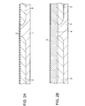
- Figure 1 is a cross-sectional view of a semiconductor device of the present embodiment.
- the semiconductor device in Fig. 1 is a LOD (LOCOS offset drain) LD (lateral double-diffused) MOS transistor.
- a p-type buried layer is formed in a p-type substrate 1.
- the p-type buried layer 3 is not formed just below an n + -type drain region 25 but is formed in a pattern surrounding the n + -type drain region 25 in a top view.
- an n-type epitaxial layer 4 is formed, an n + -type source region 24 is formed in a p-well 7 formed in the n-type epitaxial layer 4, and an n + -type drain region 25 is formed in an n-well 9 formed in the n-type epitaxial layer 4.
- the p-well 7 and the n + -type drain region 25 are separated from each other by an element isolation layer 11.
- a gate electrode 15 composed of polycrystalline silicon is formed on the n-type epitaxial layer 4 via the element isolation layer 11 or a gate oxide 12.
- contact holes 26 are formed in an interlayer insulator 22.
- a source electrode 27 and a drain electrode 28 are formed in them respectively.
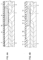
- an oxide layer (a SiO 2 layer) 2 is formed at the surface of the p-type substrate 1 by steam-oxidation at about 900 to 1000°C at a thickness of 60 to 100 nm.
- a photoresist (not shown) having an opening at the p-type buried layer 3 forming region is formed on the SiO 2 layer 2 by the known photolithography and ions are implanted using the photoresist as a mask to introduce boron (B) of about 1 X 10 13 to 1 X 10 14 atoms/cm 2 in dosage.
- the p-type buried layer 3 is not formed just below the n + -type drain region 25 but is formed in a pattern surrounding the n + -type drain region 25 in a top view. Due to this, it is made possible to cause complete depletion of a drift region without increasing the drift region length (shown as L in Fig. 8) and to improve the breakdown voltage of the transistor without increasing the on-resistance.
- the photoresist is removed and boron is diffused by heat treatment at about 1100 to 1200° C to form the p-type buried layer 3.
- the SiO 2 layer 2 on the p-type substrate 1 is removed using a hydrofluoric acid (HF) solution and then the n-type epitaxial layer 4 is formed on the p-type substrate 1 at a resistivity of about 5 to 10 ⁇ •cm.
- the thickness of the n-type epitaxial layer 4 is determined, in accordance with the desired breakdown voltage, by the general standard of about 10 ⁇ m per 100V.
- a SiO 2 layer 5 is formed at the surface of the n-type epitaxial layer 4 by steam-oxidation at about 900 to 1000°C to a thickness of 60 to 100 nm.
- a photoresist 6 having an opening at the active region of the MOS transistor is formed by the known photolithography technique.
- a p-type impurity such as boron is ion-implanted into the active region of the MOS transistor (p-well forming region 7') at about 1 X 10 12 to 1 X 10 13 atoms/cm 2 in dosage.
- the photoresist 6 is removed.
- a photoresist 8 having an opening at an n-type drift region of the MOS transistor is formed by the known photolithography technique.
- an n-type impurity such as phosphorus is ion-implanted into an n-type drift region of the MOS transistor (n-well forming region 9') by about 5 X 10 12 to 1 X 10 13 atoms/cm 2 in dosage.
- the photoresist 8 is removed.
- a silicon nitride layer (Si 3 N 4 layer) 10 is formed over the entire surface by a low-pressure CVD process, for example, to a thickness of about 80 to 100 nm.
- the boron introduced in the active region and the phosphorus introduced in the n-type drift region are diffused by heat treatment (annealing) at about 1100 to 1200° C to form the p-well 7 and the n-well 9 respectively.
- the Si 3 N 4 layer 10 is left only on the active regions and the Si 3 N 4 layer 10 in the other regions is removed by RIE (reactive ion etching), for example.
- the LOCOS 11 composed of an oxide layer is formed by steam-oxidation at about 950 to 1000° C to a thickness of about 500 to 700 nm.
- the Si 3 N 4 layer 10 is removed with hot phosphoric acid and the SiO 2 layer 5 at the surface of the n-type epitaxial layer 4 is removed using a hydrofluoric acid (HF) solution.
- RIE reactive ion etching
- the gate oxide 12 is formed at the surface of the n-type epitaxial layer 4 by steam-oxidation at 950 to 1000° C to a thickness of about 20 to 50 nm.
- a polycrystalline silicon layer 13 is formed by the CVD process to a thickness of about 400 nm.
- an n-type impurity is introduced into the polycrystalline silicon 13 by ion-implantation or thermal diffusion from a PSG (phosphosilicate glass) layer (not shown) formed on the polycrystalline silicon layer 13.
- a photoresist 14 having a pattern of the gate electrode is formed by the known photolithography on the polycrystalline silicon layer 13.
- the polycrystalline silicon layer 13 and the gate oxide 12 are etched by the known etching process such as RIE using the photoresist 14 as a mask to form the gate electrode 15. After this, the photoresist 14 is removed.
- An oxide layer (SiO 2 layer) 16 is formed by steam-oxidation at 800 to 900° C at the surface of the n-type epitaxial layer 4 except the region where the gate electrode 15 is formed and at the surface of the gate electrode 15 to a thickness of about 10 to 20 nm.
- a photoresist 17 is formed by the known photolithography and then about 1 X 10 15 to 1 X 10 16 /cm 2 of boron (B) is ion-implanted into a p-well plug region. Due to this, a p + -type source impurity-implanted region 18 is formed. After this, the photoresist 17 is removed.
- a photoresist 19 having openings at an n + -type source forming region and at an n + -type drain forming region is formed by the known photolithography technique.
- the photoresist 19 as a mask, about 1 X 10 15 to 1 X 10 16 /cm 2 of arsenic (As) is ion-implanted into the n + -type source forming region and the n + -type drain forming region. Due to this, an n + -type source impurity-implanted region 20 and an n + -type drain impurity-implanted region 21 are formed.
- the n + -type source region is formed by self-alignment using the gate electrode 15 as a mask. Therefore, it is possible to prevent any effect being felt by mask misalignment such as occurring when patterning a mask for ion-implantation by the photolithography process and therefore to perform the process precisely.
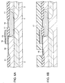
- the photoresist 19 is removed, then the interlayer insulator (SiO 2 layer) 22 is deposited over the entire surface by the CVD process to a thickness of about 600 nm.
- heat treatment is performed at about 850 to 950° C and both the boron in the p + -type source impurity-implanted region 18 and the arsenic in the n + -type source impurity-implanted region 20 and the n + -type drain impurity-implanted region 21 are diffused to form a p + -type source region (the p-well plug region) 23, the n + -type source region 24, and the n + -type drain region 25.
- a photoresist (not shown) is formed by the known photolithography process on the interlayer insulator 22, and RIE, for example, is performed using the photoresist as a mask. Due to this, as shown in Fig. 1, contact holes 26 connecting to the source region 23, 24, the drain region 25, or the gate electrode 15 are formed in the interlayer insulator 22.
- a metal layer composed of Al or Al alloy and the like is vapor deposited in the contact holes 26 formed in the interlayer insulator 22.
- a barrier metal layer composed of Ti/TiON/Ti etc. may be formed before the Al or Al alloy layer is formed.
- the metal layer is patterned by the known photolithography and RIE to form the source electrode 27 and the drain electrode 28.
- a depletion layer at the junction of the p-type buried layer 3 and the n-type epitaxial layer 4 reaches the surface of the drift region before a depletion layer at the junction of the p-type substrate 1 and the n-type epitaxial layer 4 reaches the n + -type drain region 25. Therefore, it is made possible to cause complete depletion of the drift region and to raise the breakdown voltage of a transistor. Also, according to the semiconductor device of the present embodiment, it is not necessary to increase the drift region length and it is possible to prevent an increase in the on-resistance.
- a buried layer of the same conductivity type as a semiconductor substrate and having a higher concentration of impurity than the semiconductor substrate, in a surrounding pattern around the drain region except just below the drain region in a top view. Due to this, it is made possible to produce a semiconductor device improved in the junction breakdown voltage.
- the semiconductor device and the method of producing the same of the present invention are not limited to the above embodiments.
- the semiconductor device of the present invention it is possible to cause complete depletion of the drift region without increasing the length of the second conductivity type impurity diffusion layer (the drift region length) and to achieve both of an improvement in the junction breakdown voltage and a decrease of the on-resistance.
- the method of producing a semiconductor device of the present invention it is possible to produce a semiconductor device capable of causing complete depletion of the drift region.
Landscapes
- Insulated Gate Type Field-Effect Transistor (AREA)
- Metal-Oxide And Bipolar Metal-Oxide Semiconductor Integrated Circuits (AREA)
Abstract
Description
Claims (13)
- A semiconductor device comprising:a first conductivity type semiconductor substrate;a second conductivity type semiconductor layer formed on the, first conductivity type semiconductor substrate;a first conductivity type impurity diffusion layer formed in a surface region of the second conductivity type semiconductor layer;a second conductivity type source region formed in a surface region of the first conductivity type impurity diffusion layer;a second conductivity type drain region formed in the surface region of the second conductivity type semiconductor layer at a predetermined distance from the first conductivity type impurity diffusion layer;an element isolating insulation layer formed between the second conductivity type source region and the second conductivity type drain region;a gate insulating film formed between the second conductivity type source region and the second conductivity type drain region; anda gate electrode formed on the gate insulating film, whereina buried layer containing an impurity of the first conductivity type in a higher concentration than that of the first conductivity type semiconductor substrate is formed at least in part in the surface layer of the first conductivity type semiconductor substrate except just below the second conductivity type drain region.
- A semiconductor device as set forth in claim 1, wherein the buried layer is formed in a pattern surrounding the second conductivity type drain region except just below the second conductivity type drain region.
- A semiconductor device as set forth in claim 1, wherein:further provision is made of a second conductivity type impurity diffusion layer formed via a junction with the first conductivity type impurity diffusion layer in the surface layer of the second conductivity type semiconductor layer; andthe second conductivity type drain region is formed in the surface layer of the second conductivity type impurity diffusion layer at a predetermined distance from the first conductivity type impurity diffusion layer.
- A semiconductor device as set forth in claim 1, wherein the gate electrode is composed of polycrystalline silicon.
- A semiconductor device as set forth in claim 1, wherein the first conductivity type is a p-type while the second conductivity type is an n-type.
- A semiconductor device as set forth in claim 1, wherein the second conductivity type semiconductor layer is an epitaxial layer.
- A semiconductor device as set forth in claim 1, wherein the gate insulating film is a silicon oxide film.
- A method of producing a semiconductor device comprising the steps of:introducing a first conductivity type impurity into a surface layer of a first conductivity type semiconductor substrate to form a first conductivity type buried layer containing an impurity in a higher concentration than that of the first conductivity type semiconductor substrate;growing epitaxially a second conductivity type semiconductor layer on the first conductivity type semiconductor substrate;forming a first conductivity type impurity diffusion layer connected to the first conductivity type buried layer in the surface layer of the second conductivity type semiconductor layer;forming an element isolating insulation layer partly in the second conductivity type semiconductor layer;forming a second conductivity type source region in the surface layer of the first conductivity type impurity diffusion layer;forming a second conductivity type drain region in the surface layer of the second conductivity type semiconductor layer outside a region beneath which the first conductivity type buried layer is formed;forming a gate insulating film between the second conductivity type source region and the second conductivity type drain region and forming a gate electrode on the gate insulating film; andforming a source electrode and a drain electrode connected to the source region or the drain region respectively.
- A method of producing a semiconductor device as set forth in claim 8, wherein further provision is made of a step of forming a second conductivity type impurity diffusion layer comprising the second conductivity type drain region in the surface layer of the second conductivity semiconductor layer.
- A method of producing a semiconductor device as set forth in claim 8, wherein the gate electrode is composed of polycrystalline silicon.
- A method of producing a semiconductor device as set forth in claim 8, wherein the first conductivity type is a p-type while the second conductivity type is an n-type.
- A method of producing a semiconductor device as set forth in claim 8, wherein the gate insulating film is a silicon oxide film.
- A method of producing a semiconductor device as set forth in claim 8, wherein the element isolating insulation layer is formed between the second conductivity type source region and the second conductivity type drain region.
Applications Claiming Priority (2)
| Application Number | Priority Date | Filing Date | Title |
|---|---|---|---|
| JP5577099 | 1999-03-03 | ||
| JP11055770A JP2000252465A (en) | 1999-03-03 | 1999-03-03 | Semiconductor device and manufacturing method thereof |
Publications (2)
| Publication Number | Publication Date |
|---|---|
| EP1033760A2 true EP1033760A2 (en) | 2000-09-06 |
| EP1033760A3 EP1033760A3 (en) | 2003-10-29 |
Family
ID=13008117
Family Applications (1)
| Application Number | Title | Priority Date | Filing Date |
|---|---|---|---|
| EP00103907A Withdrawn EP1033760A3 (en) | 1999-03-03 | 2000-02-24 | High withstand voltage MOS transistor and method of producing the same |
Country Status (3)
| Country | Link |
|---|---|
| US (1) | US6404009B1 (en) |
| EP (1) | EP1033760A3 (en) |
| JP (1) | JP2000252465A (en) |
Cited By (1)
| Publication number | Priority date | Publication date | Assignee | Title |
|---|---|---|---|---|
| CN102074578A (en) * | 2009-11-05 | 2011-05-25 | 夏普株式会社 | Semiconductor device and method for producing the same |
Families Citing this family (25)
| Publication number | Priority date | Publication date | Assignee | Title |
|---|---|---|---|---|
| JP2001094094A (en) * | 1999-09-21 | 2001-04-06 | Hitachi Ltd | Semiconductor device and method of manufacturing the same |
| JP2002314066A (en) * | 2001-04-13 | 2002-10-25 | Sanyo Electric Co Ltd | MOS semiconductor device and method of manufacturing the same |
| US7221011B2 (en) * | 2001-09-07 | 2007-05-22 | Power Integrations, Inc. | High-voltage vertical transistor with a multi-gradient drain doping profile |
| US7786533B2 (en) * | 2001-09-07 | 2010-08-31 | Power Integrations, Inc. | High-voltage vertical transistor with edge termination structure |
| US6635544B2 (en) * | 2001-09-07 | 2003-10-21 | Power Intergrations, Inc. | Method of fabricating a high-voltage transistor with a multi-layered extended drain structure |
| US6737311B2 (en) * | 2001-09-26 | 2004-05-18 | Agere Systems Inc. | Semiconductor device having a buried layer for reducing latchup and a method of manufacture therefor |
| CA2458992A1 (en) * | 2002-10-25 | 2004-04-25 | Shindengen Electric Manufacturing Co., Ltd. | Lateral short-channel dmos, method of manufacturing the same, and semiconductor device |
| JP2004335990A (en) | 2003-03-10 | 2004-11-25 | Fuji Electric Device Technology Co Ltd | MIS type semiconductor device |
| JP4477309B2 (en) * | 2003-05-09 | 2010-06-09 | Necエレクトロニクス株式会社 | High breakdown voltage semiconductor device and manufacturing method thereof |
| JP4711636B2 (en) * | 2004-03-12 | 2011-06-29 | パナソニック株式会社 | Manufacturing method of semiconductor device |
| US7476591B2 (en) | 2006-10-13 | 2009-01-13 | Taiwan Semiconductor Manufacturing Company, Ltd. | Lateral power MOSFET with high breakdown voltage and low on-resistance |
| US7557406B2 (en) * | 2007-02-16 | 2009-07-07 | Power Integrations, Inc. | Segmented pillar layout for a high-voltage vertical transistor |
| US7859037B2 (en) | 2007-02-16 | 2010-12-28 | Power Integrations, Inc. | Checkerboarded high-voltage vertical transistor layout |
| US7595523B2 (en) | 2007-02-16 | 2009-09-29 | Power Integrations, Inc. | Gate pullback at ends of high-voltage vertical transistor structure |
| US7468536B2 (en) | 2007-02-16 | 2008-12-23 | Power Integrations, Inc. | Gate metal routing for transistor with checkerboarded layout |
| US8653583B2 (en) | 2007-02-16 | 2014-02-18 | Power Integrations, Inc. | Sensing FET integrated with a high-voltage transistor |
| JP2009231811A (en) * | 2008-02-27 | 2009-10-08 | Seiko Instruments Inc | Semiconductor device and method of manufacturing the same |
| JP5784512B2 (en) * | 2012-01-13 | 2015-09-24 | 株式会社東芝 | Semiconductor device |
| JP5860161B2 (en) * | 2012-10-16 | 2016-02-16 | 旭化成エレクトロニクス株式会社 | Field effect transistor and semiconductor device |
| US9543396B2 (en) | 2013-12-13 | 2017-01-10 | Power Integrations, Inc. | Vertical transistor device structure with cylindrically-shaped regions |
| US10325988B2 (en) | 2013-12-13 | 2019-06-18 | Power Integrations, Inc. | Vertical transistor device structure with cylindrically-shaped field plates |
| CN110649082B (en) * | 2015-04-01 | 2024-05-14 | 群创光电股份有限公司 | Display panel |
| US10014408B1 (en) * | 2017-05-30 | 2018-07-03 | Vanguard International Semiconductor Corporation | Semiconductor devices and methods for forming the same |
| CN110164964A (en) * | 2018-02-12 | 2019-08-23 | 中芯国际集成电路制造(北京)有限公司 | Semiconductor structure and forming method thereof |
| JP2023007804A (en) * | 2021-07-02 | 2023-01-19 | キヤノン株式会社 | Light emitting device, display, photoelectric conversion device, electronic apparatus, lighting device, movable body, wearable device, and image forming apparatus |
Family Cites Families (6)
| Publication number | Priority date | Publication date | Assignee | Title |
|---|---|---|---|---|
| US4300150A (en) * | 1980-06-16 | 1981-11-10 | North American Philips Corporation | Lateral double-diffused MOS transistor device |
| US4939566A (en) * | 1987-10-30 | 1990-07-03 | North American Philips Corporation | Semiconductor switch with parallel DMOS and IGT |
| US5237193A (en) * | 1988-06-24 | 1993-08-17 | Siliconix Incorporated | Lightly doped drain MOSFET with reduced on-resistance |
| US5161686A (en) * | 1989-04-14 | 1992-11-10 | Kimberly-Clark Corporation | Odor-absorbing web material and medical material packages containing the web material |
| US5736766A (en) * | 1994-12-12 | 1998-04-07 | Texas Instruments Incorporated | Medium voltage LDMOS device and method of fabrication |
| US6207994B1 (en) * | 1996-11-05 | 2001-03-27 | Power Integrations, Inc. | High-voltage transistor with multi-layer conduction region |
-
1999
- 1999-03-03 JP JP11055770A patent/JP2000252465A/en active Pending
-
2000
- 2000-02-24 EP EP00103907A patent/EP1033760A3/en not_active Withdrawn
- 2000-02-28 US US09/514,591 patent/US6404009B1/en not_active Expired - Fee Related
Cited By (2)
| Publication number | Priority date | Publication date | Assignee | Title |
|---|---|---|---|---|
| CN102074578A (en) * | 2009-11-05 | 2011-05-25 | 夏普株式会社 | Semiconductor device and method for producing the same |
| CN102074578B (en) * | 2009-11-05 | 2013-08-21 | 夏普株式会社 | Semiconductor device and method for producing the same |
Also Published As
| Publication number | Publication date |
|---|---|
| JP2000252465A (en) | 2000-09-14 |
| EP1033760A3 (en) | 2003-10-29 |
| US6404009B1 (en) | 2002-06-11 |
Similar Documents
| Publication | Publication Date | Title |
|---|---|---|
| US6404009B1 (en) | Semiconductor device and method of producing the same | |
| US6855581B2 (en) | Method for fabricating a high-voltage high-power integrated circuit device | |
| US9466700B2 (en) | Semiconductor device and method of fabricating same | |
| US5055896A (en) | Self-aligned LDD lateral DMOS transistor with high-voltage interconnect capability | |
| US7608513B2 (en) | Dual gate LDMOS device fabrication methods | |
| US5482871A (en) | Method for forming a mesa-isolated SOI transistor having a split-process polysilicon gate | |
| US6770529B2 (en) | EDMOS device having a lattice type drift region and method of manufacturing the same | |
| US6869847B2 (en) | Semiconductor device manufacturing method thereof | |
| US20140332846A1 (en) | Transistor-type protection device, semiconductor integrated circuit, and manufacturing method of the same | |
| JPH06318697A (en) | Dmos structure and preparation thereof | |
| US7649222B2 (en) | Semiconductor device | |
| US11038051B2 (en) | Semiconductor device and method of manufacturing the same | |
| US6489657B1 (en) | Semiconductor device with improved channel stopper | |
| KR100368847B1 (en) | Insulated gate semiconductor device and its manufacturing method | |
| US20020117714A1 (en) | High voltage MOS transistor | |
| KR100306744B1 (en) | Manufacturing method of trench gate power device | |
| JP4378781B2 (en) | Semiconductor device and manufacturing method thereof | |
| JPH11317519A (en) | Semiconductor device and manufacturing method thereof | |
| JP2010212423A (en) | Semiconductor device and manufacturing method thereof | |
| JPH11297996A (en) | Semiconductor device and manufacturing method thereof | |
| JPH10190002A (en) | High-voltage device with insulated gate pinch-off structure | |
| JPH11191624A (en) | Method of manufacturing high voltage power device | |
| KR100343790B1 (en) | High voltage device having the well extended into the drift region | |
| US20220130969A1 (en) | Power device with a contact hole on a sloped ild region | |
| KR100199032B1 (en) | Manufacturing method of power device |
Legal Events
| Date | Code | Title | Description |
|---|---|---|---|
| PUAI | Public reference made under article 153(3) epc to a published international application that has entered the european phase |
Free format text: ORIGINAL CODE: 0009012 |
|
| AK | Designated contracting states |
Kind code of ref document: A2 Designated state(s): AT BE CH CY DE DK ES FI FR GB GR IE IT LI LU MC NL PT SE |
|
| AX | Request for extension of the european patent |
Free format text: AL;LT;LV;MK;RO;SI |
|
| PUAL | Search report despatched |
Free format text: ORIGINAL CODE: 0009013 |
|
| AK | Designated contracting states |
Kind code of ref document: A3 Designated state(s): AT BE CH CY DE DK ES FI FR GB GR IE IT LI LU MC NL PT SE |
|
| AX | Request for extension of the european patent |
Extension state: AL LT LV MK RO SI |
|
| RIC1 | Information provided on ipc code assigned before grant |
Ipc: 7H 01L 29/10 B Ipc: 7H 01L 21/336 B Ipc: 7H 01L 29/78 A |
|
| 17P | Request for examination filed |
Effective date: 20040329 |
|
| AKX | Designation fees paid |
Designated state(s): DE FR NL |
|
| STAA | Information on the status of an ep patent application or granted ep patent |
Free format text: STATUS: THE APPLICATION HAS BEEN WITHDRAWN |
|
| 18W | Application withdrawn |
Effective date: 20060113 |