EP1032960B1 - Antennenanordnung für eine einzelne frequenz - Google Patents
Antennenanordnung für eine einzelne frequenz Download PDFInfo
- Publication number
- EP1032960B1 EP1032960B1 EP98956085A EP98956085A EP1032960B1 EP 1032960 B1 EP1032960 B1 EP 1032960B1 EP 98956085 A EP98956085 A EP 98956085A EP 98956085 A EP98956085 A EP 98956085A EP 1032960 B1 EP1032960 B1 EP 1032960B1
- Authority
- EP
- European Patent Office
- Prior art keywords
- antenna
- arrangement
- contour
- antenna arrangement
- frequency antenna
- Prior art date
- Legal status (The legal status is an assumption and is not a legal conclusion. Google has not performed a legal analysis and makes no representation as to the accuracy of the status listed.)
- Expired - Lifetime
Links
Images

Classifications
-
- H—ELECTRICITY
- H01—ELECTRIC ELEMENTS
- H01Q—ANTENNAS, i.e. RADIO AERIALS
- H01Q1/00—Details of, or arrangements associated with, antennas
- H01Q1/36—Structural form of radiating elements, e.g. cone, spiral, umbrella; Particular materials used therewith
- H01Q1/38—Structural form of radiating elements, e.g. cone, spiral, umbrella; Particular materials used therewith formed by a conductive layer on an insulating support
-
- H—ELECTRICITY
- H01—ELECTRIC ELEMENTS
- H01Q—ANTENNAS, i.e. RADIO AERIALS
- H01Q1/00—Details of, or arrangements associated with, antennas
- H01Q1/12—Supports; Mounting means
- H01Q1/22—Supports; Mounting means by structural association with other equipment or articles
- H01Q1/24—Supports; Mounting means by structural association with other equipment or articles with receiving set
- H01Q1/241—Supports; Mounting means by structural association with other equipment or articles with receiving set used in mobile communications, e.g. GSM
- H01Q1/242—Supports; Mounting means by structural association with other equipment or articles with receiving set used in mobile communications, e.g. GSM specially adapted for hand-held use
- H01Q1/243—Supports; Mounting means by structural association with other equipment or articles with receiving set used in mobile communications, e.g. GSM specially adapted for hand-held use with built-in antennas
-
- H—ELECTRICITY
- H01—ELECTRIC ELEMENTS
- H01Q—ANTENNAS, i.e. RADIO AERIALS
- H01Q21/00—Antenna arrays or systems
- H01Q21/06—Arrays of individually energised antenna units similarly polarised and spaced apart
- H01Q21/08—Arrays of individually energised antenna units similarly polarised and spaced apart the units being spaced along or adjacent to a rectilinear path
- H01Q21/10—Collinear arrangements of substantially straight elongated conductive units
-
- H—ELECTRICITY
- H01—ELECTRIC ELEMENTS
- H01Q—ANTENNAS, i.e. RADIO AERIALS
- H01Q9/00—Electrically-short antennas having dimensions not more than twice the operating wavelength and consisting of conductive active radiating elements
- H01Q9/04—Resonant antennas
- H01Q9/0407—Substantially flat resonant element parallel to ground plane, e.g. patch antenna
- H01Q9/0421—Substantially flat resonant element parallel to ground plane, e.g. patch antenna with a shorting wall or a shorting pin at one end of the element
Definitions
- the present invention relates to a microstrip arrangement, preferably a single-frequency antenna arrangement for use within the microwave range.
- Microstrip technology is commonly used in arrangements within higher frequency ranges, for example the microwave range.
- Microstrip arrangements usually comprise a plane layer of an electrically conductive material arranged on a substrate of dielectric material.
- a common area of application for microstrip arrangements is antennas.
- the material that is used as the dielectric substrate is extremely important in known microstrip arrangements on account of inter alia the field losses that occur in the dielectric. In order to minimize these field losses, it has been necessary to use dielectric materials that are relatively expensive in previously known microstrip arrangements.
- a further problem may be material variations between different deliveries of one and the same dielectric material from one and the same manufacturer.
- One known way of reducing the field losses in the dielectric substrate in a microstrip arrangement is to provide the electrically conductive material with a non-plane shape.
- a disadvantage of this solution is that a non-plane shape drives up the manufacturing cost. Certain losses also occur in the electrically conductive material itself, compared with when the material is of plane shape.
- reflection losses Another type of loss that may arise on account of the properties of the dielectric material is reflection losses, in other words losses at the point where the microstrip arrangement is connected to other equipment, in the case of an antenna especially transmitting or receiving equipment.
- One problem that is solved by means of the present invention is therefore that of minimizing, in an arrangement made using microstrip technology, preferably a single-frequency antenna arrangement, the field losses that are caused by the dielectric material on which the conductive material is arranged.
- Another problem that is solved by means of the present invention is that of minimizing the influence of material variations in the dielectric material in a microstrip arrangement, preferably a single-frequency antenna arrangement.
- a further problem that is solved by means of the present invention is that of reducing the reflection losses that arise in a microstrip arrangement, preferably a single-frequency antenna arrangement.
- a single-frequency antenna arrangement that comprises a dielectric substrate, a first antenna contour located on one side of the dielectric substrate and a second antenna contour located on the second side of the dielectric substrate.
- the first and the second antenna contours have essentially the same dimensions in the longitudinal direction and the transverse direction, are galvanically interconnected by means of at least one connection, and extend essentially parallel to one another on either side of the dielectric material.
- the arrangement also comprises a feed point for the antenna contours, and also a ground plane which is preferably located on that side of the antenna arrangement towards which the antenna arrangement is not intended to radiate.
- the first and the second antenna contours are designed as a group of radiating elements which are interconnected with the aid of connecting lines.
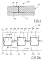
- Fig. 1 shows a diagrammatic cross-section of a single-frequency antenna arrangement 100 according to the invention, seen from the front in the longitudinal direction of the arrangement 100.
- the invention comprises a first and a second antenna contour 130, 140 located on either side of a dielectric substrate 120.
- the first and the second antenna contours 130, 140 have essentially the same dimensions in the longitudinal direction and the transverse direction, extend essentially parallel to one another on either side of the dielectric material 120 and are, in relation to one another, symmetrically located on either side of the dielectric substrate 120.
- the antenna arrangement 100 also comprises a galvanic connection 150 between the first and the second antenna contours 130, 140, shown in Fig. 1 as a connection 150 that extends, symmetrically in relation to the two antenna contours 130, 140, through the dielectric substrate 120.
- a suitable type of connection is via holes, in other words holes that are made by means of, for example, mechanical drilling, laser drilling or etching, and are then made electrically conductive by plating with an electrically conductive material.
- connection 150 The symmetrical positioning of the connection 150, and the fact that it extends through the dielectric substrate 120, are to be seen only as examples of its positioning.
- the connection 150 may be positioned in a great many other positions in relation to the antenna contours 130, 140 and the dielectric substrate 120, which will be described in greater detail below.
- the antenna arrangement 100 suitably also includes a ground plane 110, located on one side of and parallel to one antenna contour 140.
- the ground plane 110 will be shown as separated from the most closely located antenna contour 140 with the aid of dielectric material that covers it completely. Further possibilities are, for example, distance pieces made of dielectric material or an arrangement in which the antenna contours 130, 140 are, with their dielectric material 120, inserted into a groove in a structure which itself constitutes a ground plane.
- Fig. 2a shows an antenna arrangement 200 according to a preferred embodiment of the invention, seen from above.
- each antenna contour comprises a number of radiating elements 205, 215, 225 which are interconnected by means of preferably straight connections 235, 245.
- the antenna contours have essentially the same dimensions in the longitudinal direction and the transverse direction, extend essentially parallel to one another on either side of a dielectric material and are, in relation to one another, symmetrically located on either side of the dielectric material.
- connections 235, 245 between the radiating elements 205, 215, 225 are suitably connected to the radiating elements in a centred manner in relation to the extension of the respective antenna contour in the longitudinal direction.
- Fig. 2a also comprises a feed point 260 and a ground connection point 270, which will be described in greater detail below with reference to Fig. 3.
- the antenna arrangement 200 may consist of an, on the whole, arbitrary number of radiating elements.
- the radiating elements may be designed in a great many different geometrical shapes, but in the preferred embodiment shown in Fig. 2a they consist of rectangular patches 205, 215, 225.
- connection between the two antenna contours may also be designed in a great many different ways.
- Fig. 2a shows an example in which the connections consist of via holes 255, 265, 275, 285, 295, 298 positioned adjacently to the edges of the patches located in the longitudinal direction of the contours, along a line that constitutes an imaginary centre line in the longitudinal direction of the two antenna contours.
- the connections should not be located further from one another than ⁇ /8, where ⁇ is the centre frequency in the waveband for which the antenna is intended.
- Fig. 2b shows a slightly different embodiment of the arrangement according to the invention.
- connections between the two antenna contours have been positioned on the one hand as shown in Fig. 2a and on the other hand in the corners of the radiating elements.
- An arrangement according to the invention may have connections 223 added to it in the manner shown in Fig. 2b if it is desirable to further increase the effect of the two antenna contours being interconnected.
- the additional connections are then suitably positioned in concentration points in the electric field and/or in points along the periphery of the contours.
- An alternative possibility for interconnecting the first and the second antenna contours is to have a continuous connection which preferably extends in the longitudinal direction of the contours, essentially along the length of the entire arrangement.
- a connection forms a longitudinal groove of electrically conductive material.
- a further possibility for interconnecting the first and the second antenna contours is to have one or more connections which extend(s) along all or parts of the outer edges of the contours.
- FIG. 3 shows a cross-section of the arrangement in Fig. 2a, seen from the front along section A-A.
- Fig. 3 shows a cross-section of the arrangement in Fig. 2a, seen from the front along section A-A.
- the grounding point 370 is connected to the antenna contours 330, 340 by a "tongue" which projects from the respective antenna contour. In this "tongue”, there is an aperture into which the grounding point fits.
- the feed point 360 is the point at which the antenna arrangement is connected to other equipment, in the case of an antenna especially transmitting or receiving equipment.
- Fig. 3 shows an example of the positioning of this point, namely along the same line as the via holes. It is also possible to connect the antenna arrangement indirectly via, for example, slots located in a ground plane.
- a microstrip arrangement according to the invention may be used in principle in all applications where it is desirable to minimize the influence of the dielectric material.
Landscapes
- Engineering & Computer Science (AREA)
- Computer Networks & Wireless Communication (AREA)
- Waveguide Aerials (AREA)
- Details Of Aerials (AREA)
- Variable-Direction Aerials And Aerial Arrays (AREA)
Claims (10)
- Einzelfrequenz-Antennenanordnung (100, 200), die eine Masseplatte (110, 310), einen dielektrischen Träger (120, 320), eine erste Antennenkontur (130, 330), die sich auf einer ersten Seite des dielektrischen Trägers (120, 320) befindet, und eine zweite Antennenkontur (140, 340), die sich auf einer zweiten Seite des dielektrischen Trägers (120, 320) befindet, umfasst,
dadurch gekennzeichnet, dass die erste Antennenkontur (130, 330) und die zweite Antennenkontur (140, 340):- im Wesentlichen die gleichen Maße in die Längs- und in die Querrichtung haben,- elektrisch miteinander mittels mindestens einer Verbindung (150; 255, 265, 275, 285, 295, 298; 350) verbunden sind,
wodurch die Feldverluste der Antennenanordnung (100, 200) in dem dielektrischen Träger (120, 320) minimiert werden,- auf entgegengesetzten Seiten des dielektrischen Trägers (120, 320) angeordnet sind und sich im Wesentlichen parallel zueinander erstrecken. - Einzelfrequenz-Antennenanordnung (100, 200) nach Anspruch 1, dadurch gekennzeichnet, dass jede Antennenkontur (130, 330; 140, 340) aus einer Gruppe strahlender Elemente (205, 215, 225) besteht, die untereinander mittels einer Gruppe von Verbindungsleitungen (235, 245) verbunden sind.
- Einzelfrequenz-Antennenanordnung (100, 200) nach Anspruch 2, dadurch gekennzeichnet, dass die strahlenden Elemente (205, 215, 225) im Wesentlichen rechteckig sind.
- Einzelfrequenz-Antennenanordnung (100, 200) nach einem der vorhergehenden Ansprüche,
dadurch gekennzeichnet, dass die Verbindung (150; 255, 265, 275, 285, 295, 298; 350), die die erste Antennenkontur (130, 330) mit der zweiten Antennenkontur (140, 340) verbindet, entlang einer Leitung liegt, die eine imaginäre Mittenlinie in die Längsrichtung der Antennenanordnung (100, 200) darstellt. - Einzelfrequenz-Antennenanordnung (100, 200) nach einem der Ansprüche 1 bis 4,
dadurch gekennzeichnet, dass die erste Antennenkontur (130, 330) mit der zweiten Antennenkontur (140, 340) mittels durchgehenden Bohrungen (255, 265, 275, 285, 295, 298) verbunden ist. - Einzelfrequenz-Antennenanordnung (100, 200) nach Anspruch 5, dadurch gekennzeichnet, dass die durchgehenden Bohrungen (255, 265, 275, 285, 295, 298), die verwendet werden, sich in einer maximalen Entfernung von λ/8 voneinander befinden, wobei λ die Wellenlänge ist, für welche die Antennenanordnung (100, 200) im Wesentlichen bestimmt ist.
- Einzelfrequenz-Antennenanordnung (100, 200) nach Anspruch 5 oder 6, dadurch gekennzeichnet, dass die verwendeten durchgehenden Bohrungen (255, 265, 275, 285, 295, 298) benachbart zu den Kanten der strahlenden Elemente (205, 215, 225), die in die Längsrichtung der Konturen (130, 330; 140, 340) liegen, angeordnet sind.
- Einzelfrequenz-Antennenanordnung (100, 200) gemäß Anspruch 5, dadurch gekennzeichnet, dass die durchgehenden Bohrungen (255, 265, 275, 285, 295, 298) benachbart zu den Ecken der strahlenden Elemente (205, 215, 225) angeordnet sind.
- Einzelfrequenz-Antennenanordnung (100, 200) nach Anspruch 4, dadurch gekennzeichnet, dass die erste Antennenkontur (130, 330) mit der zweiten Antennenkontur (140, 340) mittels einer durchgehenden Verbindung verbunden ist.
- Einzelfrequenz-Antennenanordnung (100, 200) nach Anspruch 1, dadurch gekennzeichnet, dass die erste Antennenkontur (130, 330) mit der zweiten Antennenkontur (140, 340) mittels einer Verbindung verbunden ist, die sich entlang der ganzen oder von Teilen der äußeren Kanten der Konturen erstreckt.
Applications Claiming Priority (3)
| Application Number | Priority Date | Filing Date | Title |
|---|---|---|---|
| SE9704295A SE9704295D0 (sv) | 1997-11-21 | 1997-11-21 | Suspended doble micro strip |
| SE9704295 | 1997-11-21 | ||
| PCT/SE1998/002093 WO1999027609A1 (en) | 1997-11-21 | 1998-11-19 | Single-frequency antenna arrangement |
Publications (2)
| Publication Number | Publication Date |
|---|---|
| EP1032960A1 EP1032960A1 (de) | 2000-09-06 |
| EP1032960B1 true EP1032960B1 (de) | 2006-02-08 |
Family
ID=20409085
Family Applications (1)
| Application Number | Title | Priority Date | Filing Date |
|---|---|---|---|
| EP98956085A Expired - Lifetime EP1032960B1 (de) | 1997-11-21 | 1998-11-19 | Antennenanordnung für eine einzelne frequenz |
Country Status (6)
| Country | Link |
|---|---|
| US (1) | US6150982A (de) |
| EP (1) | EP1032960B1 (de) |
| AU (1) | AU1268999A (de) |
| DE (1) | DE69833449T2 (de) |
| SE (1) | SE9704295D0 (de) |
| WO (1) | WO1999027609A1 (de) |
Families Citing this family (7)
| Publication number | Priority date | Publication date | Assignee | Title |
|---|---|---|---|---|
| JP2001251118A (ja) * | 2000-03-07 | 2001-09-14 | Nec Corp | 携帯無線機 |
| CN100454661C (zh) * | 2001-07-31 | 2009-01-21 | 日立麦克赛尔株式会社 | 平面天线及其制造方法 |
| WO2003015214A1 (en) * | 2001-08-10 | 2003-02-20 | Southern Methodist University | Microstrip antenna employing width discontinuities |
| JP2012085215A (ja) * | 2010-10-14 | 2012-04-26 | Panasonic Corp | アンテナ装置、電子機器 |
| US20150207236A1 (en) * | 2012-07-25 | 2015-07-23 | The University Of Melbourne | Antenna unit |
| US11233310B2 (en) * | 2018-01-29 | 2022-01-25 | The Boeing Company | Low-profile conformal antenna |
| US11276933B2 (en) | 2019-11-06 | 2022-03-15 | The Boeing Company | High-gain antenna with cavity between feed line and ground plane |
Family Cites Families (7)
| Publication number | Priority date | Publication date | Assignee | Title |
|---|---|---|---|---|
| US4521755A (en) * | 1982-06-14 | 1985-06-04 | At&T Bell Laboratories | Symmetrical low-loss suspended substrate stripline |
| FR2552938B1 (fr) * | 1983-10-04 | 1986-02-28 | Dassault Electronique | Dispositif rayonnant a structure microruban perfectionnee et application a une antenne adaptative |
| US4899164A (en) * | 1988-09-16 | 1990-02-06 | The United States Of America As Represented By The Secretary Of The Air Force | Slot coupled microstrip constrained lens |
| JP3196451B2 (ja) * | 1993-10-28 | 2001-08-06 | 株式会社村田製作所 | マイクロストリップアンテナ |
| JP3340271B2 (ja) * | 1994-12-27 | 2002-11-05 | 株式会社東芝 | 無指向性アンテナ |
| DE19614362C1 (de) * | 1996-04-11 | 1997-07-31 | Siemens Ag | Antenne für ein Diebstahlschutzsystem eines Kraftfahrzeugs |
| US5963168A (en) * | 1997-01-22 | 1999-10-05 | Radio Frequency Systems, Inc. | Antenna having double-sided printed circuit board with collinear, alternating and opposing radiating elements and microstrip transmission lines |
-
1997
- 1997-11-21 SE SE9704295A patent/SE9704295D0/xx unknown
-
1998
- 1998-11-19 DE DE69833449T patent/DE69833449T2/de not_active Expired - Lifetime
- 1998-11-19 WO PCT/SE1998/002093 patent/WO1999027609A1/en active IP Right Grant
- 1998-11-19 EP EP98956085A patent/EP1032960B1/de not_active Expired - Lifetime
- 1998-11-19 AU AU12689/99A patent/AU1268999A/en not_active Abandoned
- 1998-11-20 US US09/196,166 patent/US6150982A/en not_active Expired - Lifetime
Also Published As
| Publication number | Publication date |
|---|---|
| EP1032960A1 (de) | 2000-09-06 |
| AU1268999A (en) | 1999-06-15 |
| US6150982A (en) | 2000-11-21 |
| DE69833449T2 (de) | 2006-10-26 |
| SE9704295D0 (sv) | 1997-11-21 |
| WO1999027609A1 (en) | 1999-06-03 |
| DE69833449D1 (de) | 2006-04-20 |
Similar Documents
| Publication | Publication Date | Title |
|---|---|---|
| US6266016B1 (en) | Microstrip arrangement | |
| US5581266A (en) | Printed-circuit crossed-slot antenna | |
| JP3093715B2 (ja) | 共振器付着型マイクロストリップダイポールアンテナアレイ | |
| US6496148B2 (en) | Antenna with a conductive layer and a two-band transmitter including the antenna | |
| US4125839A (en) | Dual diagonally fed electric microstrip dipole antennas | |
| US6043785A (en) | Broadband fixed-radius slot antenna arrangement | |
| US4291312A (en) | Dual ground plane coplanar fed microstrip antennas | |
| KR100455498B1 (ko) | 프린트안테나 | |
| US4401988A (en) | Coupled multilayer microstrip antenna | |
| US6747606B2 (en) | Single or dual polarized molded dipole antenna having integrated feed structure | |
| US4590478A (en) | Multiple ridge antenna | |
| US5187490A (en) | Stripline patch antenna with slot plate | |
| KR19990007464A (ko) | 마이크로파 및 밀리미터파 애플리케이션을 위한 광대역의 인쇄 | |
| US20030112200A1 (en) | Horizontally polarized printed circuit antenna array | |
| EP1132997B1 (de) | Metalltafel-Antenne | |
| JP2003514422A (ja) | プリントアンテナ | |
| US4918457A (en) | Antenna formed of strip transmission lines with non-conductive coupling | |
| EP1032960B1 (de) | Antennenanordnung für eine einzelne frequenz | |
| EP0956614B1 (de) | Mikrostreifenleiterverteilungsarray für gruppenantenne und eine solche gruppenantenne | |
| US7009564B2 (en) | TM microstrip antenna | |
| GB2252676A (en) | Patch antenna | |
| CN210074169U (zh) | 一种基于接地共面波导的矩形微带串馈天线 | |
| CN108666747B (zh) | 一种低剖面阵列天线 | |
| US20100141532A1 (en) | Antenna feeding arrangement | |
| CN115207591A (zh) | 强耦合带状线和含有强耦合带状线的微波元件 |
Legal Events
| Date | Code | Title | Description |
|---|---|---|---|
| PUAI | Public reference made under article 153(3) epc to a published international application that has entered the european phase |
Free format text: ORIGINAL CODE: 0009012 |
|
| 17P | Request for examination filed |
Effective date: 20000615 |
|
| AK | Designated contracting states |
Kind code of ref document: A1 Designated state(s): DE ES FI FR GB IT |
|
| RAP1 | Party data changed (applicant data changed or rights of an application transferred) |
Owner name: TELEFONAKTIEBOLAGET LM ERICSSON (PUBL) |
|
| GRAP | Despatch of communication of intention to grant a patent |
Free format text: ORIGINAL CODE: EPIDOSNIGR1 |
|
| GRAS | Grant fee paid |
Free format text: ORIGINAL CODE: EPIDOSNIGR3 |
|
| GRAA | (expected) grant |
Free format text: ORIGINAL CODE: 0009210 |
|
| AK | Designated contracting states |
Kind code of ref document: B1 Designated state(s): DE ES FI FR GB IT |
|
| PG25 | Lapsed in a contracting state [announced via postgrant information from national office to epo] |
Ref country code: IT Free format text: LAPSE BECAUSE OF FAILURE TO SUBMIT A TRANSLATION OF THE DESCRIPTION OR TO PAY THE FEE WITHIN THE PRESCRIBED TIME-LIMIT;WARNING: LAPSES OF ITALIAN PATENTS WITH EFFECTIVE DATE BEFORE 2007 MAY HAVE OCCURRED AT ANY TIME BEFORE 2007. THE CORRECT EFFECTIVE DATE MAY BE DIFFERENT FROM THE ONE RECORDED. Effective date: 20060208 |
|
| REG | Reference to a national code |
Ref country code: GB Ref legal event code: FG4D |
|
| REF | Corresponds to: |
Ref document number: 69833449 Country of ref document: DE Date of ref document: 20060420 Kind code of ref document: P |
|
| PG25 | Lapsed in a contracting state [announced via postgrant information from national office to epo] |
Ref country code: ES Free format text: LAPSE BECAUSE OF FAILURE TO SUBMIT A TRANSLATION OF THE DESCRIPTION OR TO PAY THE FEE WITHIN THE PRESCRIBED TIME-LIMIT Effective date: 20060519 |
|
| ET | Fr: translation filed | ||
| PLBE | No opposition filed within time limit |
Free format text: ORIGINAL CODE: 0009261 |
|
| STAA | Information on the status of an ep patent application or granted ep patent |
Free format text: STATUS: NO OPPOSITION FILED WITHIN TIME LIMIT |
|
| 26N | No opposition filed |
Effective date: 20061109 |
|
| PGFP | Annual fee paid to national office [announced via postgrant information from national office to epo] |
Ref country code: FI Payment date: 20071129 Year of fee payment: 10 Ref country code: IT Payment date: 20071128 Year of fee payment: 10 |
|
| PG25 | Lapsed in a contracting state [announced via postgrant information from national office to epo] |
Ref country code: FI Free format text: LAPSE BECAUSE OF NON-PAYMENT OF DUE FEES Effective date: 20081119 |
|
| PG25 | Lapsed in a contracting state [announced via postgrant information from national office to epo] |
Ref country code: IT Free format text: LAPSE BECAUSE OF NON-PAYMENT OF DUE FEES Effective date: 20081119 |
|
| REG | Reference to a national code |
Ref country code: DE Ref legal event code: R082 Ref document number: 69833449 Country of ref document: DE Representative=s name: GRUENECKER, KINKELDEY, STOCKMAIR & SCHWANHAEUS, DE |
|
| REG | Reference to a national code |
Ref country code: DE Ref legal event code: R082 Ref document number: 69833449 Country of ref document: DE Representative=s name: GRUENECKER, KINKELDEY, STOCKMAIR & SCHWANHAEUS, DE |
|
| REG | Reference to a national code |
Ref country code: DE Ref legal event code: R082 Ref document number: 69833449 Country of ref document: DE Representative=s name: GRUENECKER PATENT- UND RECHTSANWAELTE PARTG MB, DE Effective date: 20150126 Ref country code: DE Ref legal event code: R082 Ref document number: 69833449 Country of ref document: DE Representative=s name: GRUENECKER PATENT- UND RECHTSANWAELTE PARTG MB, DE Effective date: 20150119 Ref country code: DE Ref legal event code: R082 Ref document number: 69833449 Country of ref document: DE Representative=s name: GRUENECKER, KINKELDEY, STOCKMAIR & SCHWANHAEUS, DE Effective date: 20150126 Ref country code: DE Ref legal event code: R082 Ref document number: 69833449 Country of ref document: DE Representative=s name: GRUENECKER, KINKELDEY, STOCKMAIR & SCHWANHAEUS, DE Effective date: 20150119 Ref country code: DE Ref legal event code: R081 Ref document number: 69833449 Country of ref document: DE Owner name: OPTIS CELLULAR TECHNOLOGY, LLC (N. D. GES. D. , US Free format text: FORMER OWNER: TELEFONAKTIEBOLAGET LM ERICSSON (PUBL), STOCKHOLM, SE Effective date: 20150119 |
|
| REG | Reference to a national code |
Ref country code: FR Ref legal event code: PLFP Year of fee payment: 18 |
|
| REG | Reference to a national code |
Ref country code: FR Ref legal event code: TP Owner name: OPTIS CELLULAR TECHNOLOGY, LLC, US Effective date: 20151223 |
|
| REG | Reference to a national code |
Ref country code: FR Ref legal event code: PLFP Year of fee payment: 19 |
|
| REG | Reference to a national code |
Ref country code: GB Ref legal event code: 732E Free format text: REGISTERED BETWEEN 20161020 AND 20161026 |
|
| REG | Reference to a national code |
Ref country code: FR Ref legal event code: PLFP Year of fee payment: 20 |
|
| PGFP | Annual fee paid to national office [announced via postgrant information from national office to epo] |
Ref country code: FR Payment date: 20171020 Year of fee payment: 20 Ref country code: DE Payment date: 20171019 Year of fee payment: 20 |
|
| PGFP | Annual fee paid to national office [announced via postgrant information from national office to epo] |
Ref country code: GB Payment date: 20171020 Year of fee payment: 20 |
|
| REG | Reference to a national code |
Ref country code: DE Ref legal event code: R071 Ref document number: 69833449 Country of ref document: DE |
|
| REG | Reference to a national code |
Ref country code: GB Ref legal event code: PE20 Expiry date: 20181118 |
|
| PG25 | Lapsed in a contracting state [announced via postgrant information from national office to epo] |
Ref country code: GB Free format text: LAPSE BECAUSE OF EXPIRATION OF PROTECTION Effective date: 20181118 |