EP1031997A1 - Système électronique fonctionnant sous irradiation, procédé de conception d'un tel système, et application de celui-ci à la commande d'un robot mobile - Google Patents
Système électronique fonctionnant sous irradiation, procédé de conception d'un tel système, et application de celui-ci à la commande d'un robot mobile Download PDFInfo
- Publication number
- EP1031997A1 EP1031997A1 EP00400473A EP00400473A EP1031997A1 EP 1031997 A1 EP1031997 A1 EP 1031997A1 EP 00400473 A EP00400473 A EP 00400473A EP 00400473 A EP00400473 A EP 00400473A EP 1031997 A1 EP1031997 A1 EP 1031997A1
- Authority
- EP
- European Patent Office
- Prior art keywords
- components
- shielding
- radiation
- analog
- vulnerable
- Prior art date
- Legal status (The legal status is an assumption and is not a legal conclusion. Google has not performed a legal analysis and makes no representation as to the accuracy of the status listed.)
- Granted
Links
Images





Classifications
-
- G—PHYSICS
- G21—NUCLEAR PHYSICS; NUCLEAR ENGINEERING
- G21F—PROTECTION AGAINST X-RADIATION, GAMMA RADIATION, CORPUSCULAR RADIATION OR PARTICLE BOMBARDMENT; TREATING RADIOACTIVELY CONTAMINATED MATERIAL; DECONTAMINATION ARRANGEMENTS THEREFOR
- G21F7/00—Shielded cells or rooms
- G21F7/06—Structural combination with remotely-controlled apparatus, e.g. with manipulators
- G21F7/065—Remotely manipulated machinery
-
- G—PHYSICS
- G21—NUCLEAR PHYSICS; NUCLEAR ENGINEERING
- G21F—PROTECTION AGAINST X-RADIATION, GAMMA RADIATION, CORPUSCULAR RADIATION OR PARTICLE BOMBARDMENT; TREATING RADIOACTIVELY CONTAMINATED MATERIAL; DECONTAMINATION ARRANGEMENTS THEREFOR
- G21F7/00—Shielded cells or rooms
- G21F7/06—Structural combination with remotely-controlled apparatus, e.g. with manipulators
- G21F7/066—Remotely manipulated tools
Definitions
- the present invention relates to a system electronics operating under irradiation, in particular X or gamma, a process for designing such a system, intended to operate this system under irradiation, while comprising components "Vulnerable", that is to say intrinsically incapable of operate under this irradiation, and the application of this method of controlling a mobile robot.
- vulnerable circuits we mean electronic circuits that support only one or only a few hundred kRad, typically in the form gamma or neutron radiation as they are nuclear engineering meeting. Generally, these circuits have a very high degree of integration (defined by the English term VLSI (“Very Large Scale Integration ”) and CMOS technology, although these characteristics are not limiting.
- the invention is therefore mainly developed for the design of control systems for nuclear environment, which are currently the best performing electronic systems working in this environment. That's why they're taken as an example for the description of an achievement privileged. But we do not go outside the framework of the invention by applying it to any other system electronic, since its complexity makes advantageous the use of "vulnerable" components to ambient irradiation.
- control system is not considered here in the very restricted sense often used in nuclear engineering, particularly due to very rudimentary performances allowed in known art, and some examples of which are provided below.
- control system is used in the broader sense that it has in automatic, to know: its purpose is to collect information on the system to be ordered, process them if necessary (for example by digital filtering, by correction of non-linearity), apply one or more laws of numerical control which can include modes of autonomous operations able to take decision, manage the amplifier commands power associated with the actuators, ensure security and manage functions, in case of failure partial, degraded operating modes.
- a such command may also be able to communicate with an information transmission device, according to possibilities of various working configurations (multiplexing, wireless transmission, or any other way).
- a first category includes command which can correspond to the definition above, but cannot bear in practice more than a few kRad, exceptionally a few dozen kRad.
- On-board electronics consists of a controller standard consisting of a microcontroller card and commercial drives. Orders are transmitted by an umbilical cord.
- the control system is conventional, close to industrial type controls, but its resistance to radiation does not exceed 1 to 10 kRad.
- a second category includes very simplified command, not being able to correspond to the definition above, but able to withstand practices several tens of kRad, even several hundreds of kRad if they have practically no electronics and if their order is deported to the end of a wire-to-wire connection.
- An example is the mobile robot "Oscar” intervention, for which all signals are transmitted wire by wire by a cord umbilical of large diameter in front of the dimensions of the robot, and whose length is necessarily limited.
- RD 500 assisted remote manipulator used on site of La Hague in the 1990s: all the signs of command are transmitted wire to wire by a cord umbilical, and the control itself is deported in non-irradiated areas.
- Systems of this second category do not can perform advanced, efficient functions, nor be autonomous and safe, security presupposing the existence of degraded modes or redundancies, as well than the ability to operate independently.
- Some components have a housing designed to resist ionizing radiation but it it is a light shield against SEUs ("Single Event Upsets ”) encountered by satellites, which are accidental collisions with particles extremely energetic, which can cause destruction local of a microcomponent. Their effectiveness against gamma radiation is insignificant, even if it is reinforced by an additional metal screen, because the cumulative dose of gamma radiation that a satellite is relatively weak (around 100 kRad for its entire lifetime) and does not constitute a goal for the designer. The skilled person knows that, despite the common designation of "radiation ionizing ", this is actually a different problem of those encountered in the nuclear industry.
- the shielding against ionizing radiation is consisting of a thick cover of heavy metal (for example of lead or Denal for radiation gamma), since the attenuation provided by this shielding depends on the atomic mass of the material.
- the curves show that the thickness must exceed several centimeters so that the shielding is significant, and that this thickness increases very rapidly as the dose is increased admissible radiation.
- Curing essentially consists of replace the MOS circuits with their equivalents, when they exist, in hardened technology (SOS, SOI, DMILL, etc ).
- SOS hardened technology
- SOI SOI
- DMILL hardened technology
- the three SOS, SOI technologies and DMILL remain little distributed commercially, hence an offer of poor components, both in terms of diversity of products in terms of performance.
- products currently available hardened have features and performance corresponding to a technological lag about 20 years compared to the components not hardened: they do not have an access memory random, and their features and instruction sets are hardly compatible with a command as defined above.
- Their outfit the irradiation is around 300 kRad, i.e. about a 10-fold improvement over a standard component, a little more compared to a model particularly vulnerable.
- a radio-controlled device for example, must be able, in if there is a transmission problem, make a decision autonomous (for example return to the previous position loss of communication).
- Another well-known example consists of introducing, via an airlock, a mobile robot into a nuclear power plant after an accident that resulted in the nuclear material leak inside the building. We know how to introduce the robot, but respect tightness prohibited from transmitting the cable controls. The robot must therefore imperatively move autonomously towards one of these points, which is currently impossible to achieve.
- the present invention relates to a system electronics operating under irradiation, in particular X or gamma, a method of designing such a system and its preferential application to a control system of mobile robot operating under this irradiation.
- Stage II which leads to choosing preferably functionally very rich circuits, has for consequence of limiting the functionality to be provided by the other components of the system. This facilitates the use other techniques than shielding to ensure their protection.
- Stage III involves the parameters which size protection.
- the shield itself is carried out according to the state of the art, in particular as regards concerns the material which must be adapted to the nature of the radiation considered.
- Stage IV mentions a list of components the most vulnerable by first taking into account their technology, then their degree of integration.
- a experienced person or using information from the constructor can establish a first hierarchy in the ability of the components to tolerate a certain dose irradiation.
- Stage V defines components intended for be selectively protected, which are components powerful and rich in functions for which it is impossible to find, in the industrial ranges usual, radiation resistant equivalents.
- the typical example is a microcontroller in technology Very High Integration CMOS (VLSI), comprising on a single semiconductor “chip”: central processing unit, memories, inputs / outputs, watchdog, etc ... retains from the list in the previous paragraph that the components, starting with the most vulnerable, which can be installed in the volume defined in paragraph III.
- the components that must be physically very close to these components such as example the clock quartz of a microcontroller or decoupling capacitor (s), theirs are associated and are a priori retained in the same way. Nevertheless we does not depart from the scope of the invention by renouncing protect these ancillary components.
- Difficulties may exist in evacuating heat generated by the operation of these components.
- we do not go outside the invention by incorporating between these components and the shielding a electrically insulating but thermally insulating product conductor, in order to evacuate the heat by the shielding.
- Step VI constitutes a validation of the components selected in the previous step, in considering the constraints linked to the operation of electronics: including number and band passing signals to circulate between components intended to be selectively protected by shielding and those intended not to be. However, we strive for these second components to improve their radiation tolerance by any other shielding (see step VIII).
- Stage VII includes the realization of the means protection or shielding.
- a realization preferential shielding consists of two half-shells secured by screws, arranged so as to minimize their impact on the protection of components.
- the connections with the second set of components can advantageously be carried out by a flexible printed circuit, which follows a chicane which is shielding at its input / output, to avoid the radiation penetration.
- Stage VIII mentions techniques for protection other than shielding, for example processes for managing the operation of these components by redundancies and / or voltage optimization supply as described in documents [1] and [2], making it possible to significantly lengthen their lifetime.
- Another example is the use of sequence of actions (in logic level) whose time ranges are wide enough to make their operation tolerant towards temporal drifts which can result from irradiation.
- a privileged application of the invention constituted by a control system control for mobile robot able to operate in a irradiated medium, and having to support 1 MRad.
- the microcontroller and the converter analog / digital are in low CMOS technology consumption and low noise, but their technology makes it very fragile to radiation. These two components have no insensitive or insensitive equivalent to radiation.
- Step III Determination of the available volume
- Step IV Classification of components by vulnerability
- Step V Components to be protected
- microcontroller and converters analog / digital must be protected. At these components should be added as additional elements to be located nearby, a clock quartz and decoupling capacitors.
- Step VI “First components” compatible with the volume allocated
- the volume available for protection is not sufficient to house the microcontroller and analog / digital converters, even when using hybridization techniques.
- Step III Determination of the available volume
- Step IV Classification of components by vulnerability
- Step V Components to be protected
- a microcontroller and a converter analog / digital both encapsulated according to the CMS technology, i.e. components for surface mounting. We associate them as elements annexes a quartz and decoupling capacitors. The multiplexer is not included among the components protected.
- Step VI “First components” compatible with the volume allocated
- the microcontroller and the converter analog are each installed on a printed circuit multilayer.
- Each of these printed circuits is connected components not shielded by a printed circuit flexible, the other end of which is a card interface of an electronic rack.
- the shield consists of two half-shells of Denal, weighing 10kg together, and whose shape exterior approaches a flattened sphere. Size of the shielding is calculated by making the ratio between the dose to be reached (1 MRad) and resistance to radiation of the most vulnerable component.
- the report for the control system is a factor of 50 protection.
- 35 mm of lead brings a factor of 10 attenuation for cobalt 60 irradiation. obtains the same result with 24 mm of Dénal.
- the first set of first components is installed on two multilayer printed circuits, but it is not outside the scope of the invention to use a single printed circuit. These two printed circuits communicate each with an interface card, belonging to the second set of components.
- the validation tests under irradiation are first performed on the first set of firsts components, provided with its shielding. Then a test under irradiation of the complete system makes it possible to verify the conformity of the whole system.
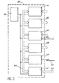
- Figure 3 shows diagrammatically the system 20, showing on the one hand the various electronic cards interfaces respectively with all or two inputs nothing 31, all or nothing outputs 32, inputs analog 33 (connected to flexible printed circuit 25), analog outputs 34, interface 35 (connected to a serial data transmission line 15), and the processor bus management interface card 37 (connected to the flexible printed circuit 23), as well as arrows 38 in double line representing traffic information between these various cards.
- She shows also the power supply board 36 which provides the voltages required at interfaces 31, 32, 33, 34, 35 and 37, as well as to module 21 via the circuits flexible prints 23 and 25.
- FIG. 4A represents a microcontroller 40, a quartz 41 and a decoupling capacitor 42, mounted on a printed circuit 24 and connected by a flexible printed circuit 23 at the interface card 33, illustrated in FIG. 3.
- the clock quartz 41 and the power decoupling capacitor 42 must be connected as close as possible to the microcontroller 40.
- Figure 4B shows a converter analog / digital 43, a decoupling capacitor 44 and an external voltage reference 45, mounted on a printed circuit 26 and connected by a printed circuit flexible 25 to the interface card 37, illustrated on the figure 3.
- the voltage reference circuit 45 and the supply decoupling capacitor 44 must be as close as possible to the analog / converter digital 43.
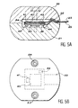
- Figures 5A and 5B show an example of shielding 22 made up of. two half-shells 50 and 51, which provide protection components 40, 41, 42, 43, 44, 45. These two half-shells constitute a shield, which we strive for here to make isotropic for the attenuation of gamma rays.
- the passage of flexible printed circuits 23 and 25, in shield input / output, has a baffle 52 preventing radiation from reaching directly said components.
- Figure 5B shows schematically a top view of the two half-shells 50 and 51, held together by screws 53, 54.
- Figure 6 shows schematically the information exchange between components selectively protected in shield 22 and the rest of the system, via interface cards 33 and 37.
- Logic located on the interface card 37, relays data, address and signal order according to a conventional scheme for a man of art via a conventional processor bus 38 (background basket).
- a logic 70 of address decoding and data exchange On this bus 38 is connected a logic 70 of address decoding and data exchange.
- This logic 70 controls the logic for selecting a entry among N of an analog multiplexer 72 of the type N: 1, connected to the N analog inputs via 73 preamplifiers / conditioners, all made in technologies known to be resistant.
- the microcontroller program 40 commands successively converting analog input signals, by successive selection of these by means of the multiplexer 72 and then retrieves the result of this analog / digital conversion via the same logic command 70 and the processor bus 38.
- FIGS. 7A and 7B represent a mode of mechanical realization of the invention.
- a rack 90 made by a metal plate, is fixed a frame classic 91, which constitutes the physical support of system 20, with a motherboard 92 whose circuit printed vehicle signals from bus 38 as well as analog lines attacking the conditioners 73, and the power lines from card 36.
- a motherboard 92 On the motherboard 92 are connected interface cards 37 processor bus management, card 33 which includes the analog multiplexing assembly 70 to 73, and the other maps 31, 32, 34, 35 36 not detailed on this figure.
- 95 cards are control cards engines not detailed.
- the shield 22 is made up of a kind of hollowed-out sphere 100 in Denial, composed of two half-shells 50 and 51, from which the printed circuits emerge flexible 23 and 25 connected to cards 33 and 37.
- This sphere 100 is maintained by two tori 98 in elastomer, made integral by a hollow plate 96 and four columns 97.
- the elastomer chosen is of polyurethane.
- the sphere 100 is thus placed on a first torus 98 in elastomer, whose inner radius is chosen so that it does not come in contact with the support plane where this first torus rests 98, even at its maximum crushing.
- a second torus 98 identical is placed above the sphere 100.
- This damping system ensures the maintenance of the assembly on the frame 90, while ensuring damping of the movements of the sphere 100 in case shock (for example in the event of a fall) or vibration in the direction perpendicular to the plane of the frame 90.
- This unit 10 and this computer 13 are interconnected by a quick link 15 of data transmission.
- actions 10 are expected from actions reflexes such as emergency stop in case anomalies such as excess current consumed by a engine, or degraded operating modes, or even autonomous.
- actions reflexes such as emergency stop in case anomalies such as excess current consumed by a engine, or degraded operating modes, or even autonomous.
- the realization of such functionalities, known to those skilled in the art, is not part of the invention.
- the invention is applicable to any electronic system in front operate under irradiation.
Landscapes
- Physics & Mathematics (AREA)
- Engineering & Computer Science (AREA)
- General Engineering & Computer Science (AREA)
- High Energy & Nuclear Physics (AREA)
- Shielding Devices Or Components To Electric Or Magnetic Fields (AREA)
- Measurement Of Radiation (AREA)
Abstract
Description
- acquérir une ou plusieurs mesures,
- éventuellement les traiter de façon rudimentaire par un filtrage analogique simple (du premier ordre), ou dans le meilleur des cas par une numérisation sous 8 bits avec des temps de conversion longs (supérieurs à 10µs),
- transmettre cette (ou ces) mesure(s) selon un protocole séquentiel figé, quand ce n'est pas directement fil à fil, ce qui pose alors le problème d'un cordon ombilical pénalisant par son diamètre, son poids, ou tout simplement son existence même (il rend impossible le franchissement d'un sas),
- envoyer des consignes vers les amplificateurs de puissance qui n'appartiennent pas à proprement parler au système de commande.
- combiner ces composants par voie d'implantation ou d'« hybridation » (montage compact de puces électroniques) pour les protéger par un unique blindage,
- affecter à la protection contre le rayonnement plusieurs blindages renfermant des composants sélectivement protégés.
- mécaniquement par une suspension amortissante,
- électriquement par des connexions suffisamment souples pour prendre en compte les déplacements dus à cette suspension mécanique.
- La figure 1 est un organigramme retraçant les diverses étapes du procédé de l'invention,
- le figure 2 représente schématiquement le système électronique de l'invention,
- la figure 3 est un schéma synoptique de l'interface représentée sur la figure 2, qui dans la réalisation décrite comporte plusieurs cartes électroniques montées dans une baie,
- les figures 4A et 4B représentent une implantation de l'ensemble des premiers composants,
- les figures 5A et 5B représentent deux vues en coupe du blindage, montrant de profil l'ensemble des premiers composants illustrés sur les figures 4A et 4B,
- la figure 6 schématise fonctionnellement les échanges d'information entre les composants sélectivement protégés dans le blindage 22 et le reste du système, via les cartes d'interface 33 et 37,
- les figures 7A et 7B illustrent un mode de réalisation mécanique de l'invention ; la figure 7A montrant l'agencement général et la figure 7B montrant un montage mécanique amortisseur de chocs et/ou vibrations pour la partie blindée,
- la figure 8 situe le système de commande selon l'invention dans le contexte global de son utilisation.
- acquisition de mesures capteur et traitement
analogique ou numérique, par exemple :
- six mesures analogiques de courant moteur,
- deux mesures analogiques de température,
- une mesure analogique de courant batterie,
- une mesure analogique de mesure de référence de tension,
- dix entrées TOR de conformité commande relais (TOR :Tout Ou Rien),
- cinq entrées TOR divers ;
- envois de commandes, par exemple :
- six commandes analogiques de moteur,
- dix sorties TOR de commande de relais,
- cinq sorties TOR annexes ;
- communication via un lien série « full
duplex » avec le poste de commande :
- interprétation des messages reçus,
- émission de messages,
- contrôle de la conformité des messages ;
- contrôle du fonctionnement du robot :
- contrôle des actions du robot,
- interprétation de la mesure des capteurs de sécurité,
- gestion de modes de sécurité (thermique,
- gestion de mode dégradé ou de mode autonome (perte de communication, actions autonome...).
- amplificateurs de ligne ("driver" en anglais), décodage d'adresse, logique trois états,
- convertisseur analogique/numérique, filtres analogiques, amplificateurs analogiques,
- convertisseurs numérique/analogique,
- composants logiques TOR, relais.
- un contrôleur 40 (comportant le processeur, une mémoire de code, une mémoire RAM ("Random Access memory"), un circuit UART ("Universal Asynchronous Receiver Transmitter"), un gestionnaire de bus, un chien de garde, et des performances élevées en rapidité de calcul),
- un convertisseur analogique/numérique 43 (incluant référence de tension, échantillonneur/ bloqueur, logique fonctionnant en mode trois états, signaux de contrôle, performances élevées en termes de résolution et de temps d'acquisition),
- des amplificateurs opérationnels (filtrage et amplification),
- des convertisseurs numérique/ analogiques incluant une référence de tension,
- des composants logiques TTL (amplificateurs de ligne, décodage d'adresse, logique trois états, composants logiques TOR) de type ALS,
- des composants passifs,
- des relais électromécaniques.
- le niveau de dose tolérable reste inférieur à 300 kRad pour la plupart des composants durcis (donnée imposée par les besoins du marché spatial, sans intérêt pour le nucléaire), ce qui revient à dire que le problème posé ne pourrait être résolu ;
- même avec une durée de vie n'excédant pas le tiers de la durée de vie spécifiée, les performances générales du système seraient inférieures de plusieurs ordres de grandeur, c'est-à-dire de dix fois à plus de cent fois selon le paramètre considéré : puissance de calcul du processeur, taille de la mémoire, débit des liaisons séries, temps de cycle processeur, vitesse du bus.
- le poids maximal admissible pour le blindage : par exemple 10 kg ;
- le matériau : par exemple pour le rayonnement gamma considéré, on choisit le Dénal, alliage de tungstène ; lors de l'étape III le plomb et le Dénal sont envisagés pour apprécier l'intérêt du Dénal par rapport au plomb, mais on ne fera pas d'itération avec le plomb pour ne pas alourdir inutilement l'exposé ;
- la dose d'irradiation tolérable : par exemple 1 MRad ;
- la distance entre les deux ensembles de composants : par exemple moins de 2 dm.
- convertisseur analogique numérique : 20 kRad,
- microcontrôleur : environ 50 kRad,
- convertisseur numérique/analogique : >1 MRad,
- amplificateur opérationnel : >1MRad,
- composants logiques TTL : >1MRad en respectant des règles de mise en oeuvre (voir étape VIII),
- composants passifs : environ 100 MRad,
- relais : > 1MRad.
- un microcontrôleur de la Société Siemens,
- un convertisseur numérique/analogique,
- un multiplexeur analogique de la Société Analog Devices,
- des amplificateurs opérationnels (filtrage et amplification),
- six convertisseurs numérique/ analogiques,
- des composants logiques en technologie TTL (amplificateurs de ligne, décodage d'adresse, logique trois états, composants logiques TOR, logique de sélection),
- composants passifs,
- relais électromécaniques.
- microcontrôleur : environ 50 kRad,
- convertisseur analogique numérique : 20 kRad,
- multiplexeur analogique >1 MRad,
- convertisseur numérique/analogique : >1 MRad,
- amplificateur opérationnel : >1 MRad,
- composants logiques TTL : >1 MRad en respectant des règles de mise en oeuvre,
- composants passifs : environ 100 MRad,
- relais : >1 MRad.
- les alimentations,
- un bus multiplexé propre au microcontrôleur (0-5V, 20 MHz),
- les signaux de commandes et de données propres au convertisseur (0-5V, 20 MHz),
- le signal d'entrée analogique du convertisseur (+/-10V,300Hz max).
- des chronogrammes d'enchaínement des actions (au niveau de la logique TTL) tolérants vis-à-vis de dérives temporelles,
- un fonctionnement dynamique de la logique TTL trois états géré par le microcontrôleur pour minimiser le courant de fuite en phase bloquée,
- une compensation logicielle de la dérive sous irradiation de la mesure du convertisseur analogique/ numérique par mesure de tensions de référence connues.
- d'un système d'interfaces 20 (comportant plusieurs cartes), équipé de composants résistants ou durcis ou tolérants,
- d'un module 21 comportant des composants industriels standards, protégé par un blindage 22, et relié au système d'interfaces 20 par un circuit imprimé souple 23, 25,
- d'une ligne 15 de transmission série de données,
- de connexions avec le robot 11 (commandes de moteurs, retour d'informations capteurs),
- d'une ligne 16 d'alimentation en énergie.
- les alimentations 63,
- le bus d'adresses et de données 64 propre au microcontrôleur 40,
- les signaux de commande et de données 65 propres au convertisseur 43,
- le signal d'entrée analogique 66 du convertisseur 43.
- une unité 10 localisée au voisinage immédiat du robot 11, et soumise au flux de radiations (milieu irradié 12),
- un ordinateur 13 au contact de l'opérateur 14, localisé en milieu non hostile.
- la scrutation des différents capteurs du robot (positions, vitesses, retour d'efforts),
- l'envoi des données des capteurs à l'ordinateur 13,
- la réception des consignes calculées par l'ordinateur 13,
- la transmission pour exécution de ces consignes aux modules d'électronique de puissance reliés aux actionneurs du robot (moteurs).
Claims (11)
- Procédé de conception d'un système électronique apte à fonctionner sous irradiation, caractérisé en ce qu'il comprend les étapes suivantes :I. énumérer l'ensemble des fonctions que doit réaliser le système.II. déterminer les composants électroniques aptes à réaliser physiquement ces fonctions, en accordant la préférence aux modèles ayant le plus fort taux d'intégration.III. déterminer le volume de composants qu'il est possible de protéger par un blindage, en tenant compte de la dose d'irradiation que doit supporter le système, du poids maximal admissible, du matériau choisi pour ce blindage, ainsi que la distance à laquelle les composants sélectivement protégés par un blindage pourront être des autres composants non blindés.IV. établir une liste des composants les plus vulnérables en tenant compte d'abord de leur technologie, puis de leur degré d'intégration, en associant à chacun de ces composants les composants qui doivent être implantés à leur proximité immédiate, s'il en existe, et en plaçant en premier le composant le plus vulnérable, puis en second celui dont la vulnérabilité est un peu moins élevée, et ainsi de suite, éventuellement en plaçant plusieurs circuits de vulnérabilités identiques.V. sélectionner à partir de la liste de l'étape précédente, un ensemble de composants, en commençant par les composants les plus vulnérables, en limitant cet ensemble aux composants qui peuvent, de par leurs dimensions, être implantés dans le volume défini lors de l'étape III.VI. examiner si les composants de cet ensemble peuvent réaliser des fonctions cohérentes et ne communiquer avec le reste du système que par un nombre raisonnable de fils, qui transmettent des signaux pouvant parcourir sans être altérés la distance prévue à l'étape III entre les composants sélectivement protégés et les autres composants ; si toutes ces conditions ne sont pas simultanément remplies, modifier par itération la liste des composants pour obtenir ce résultat, sans excéder le volume défini à l'étape III ; si toutes ces conditions sont simultanément remplies, aller à l'étape suivante ; l'ensemble de composants ainsi obtenu étant dénommé premier ensemble de premiers composants, et les autres composants étant dénommés second ensemble de seconds composants.VII. concevoir l'implantation physique du premier ensemble de premiers composants, et concevoir des moyens de protection, dénommés blindage, constitués d'au moins un matériau absorbant pour les rayonnements, disposés autour de ce premier ensemble de composants, et concevoir, entre le premier ensemble de composants et le second, des moyens de connexion agencés pour ne pas former de chemin de pénétration pour les rayonnements ambiants.VIII. concevoir l'implantation physique du second ensemble de composants, évaluer la dose de rayonnements qu'ils auront effectivement à supporter et si nécessaire, utiliser une technique complémentaire pour améliorer leur aptitude au fonctionnement sous irradiation par une technique autre que le blindage.IX. évaluer si la solution au problème posé est obtenue ; si elle n'est pas obtenue, modifier les paramètres de l'étape III et réitérer le processus à partir de cette étape III.
- Procédé selon la revendication 1, comprenant une étape ultérieure :
X. valider la conception en réalisant un prototype conforme aux étapes de conception précédentes, au moins en ce qui concerne le premier ensemble de composants, implanté et mis en place dans ses moyens de protection, et effectuer des essais d'irradiation ; si ces essais ne sont pas conformes aux spécifications, modifier les paramètres de l'étape III et réitérer le processus à partir de cette étape III. - Système électronique apte à fonctionner sous irradiation, caractérisé en ce qu'il comprend :un premier ensemble de composants comportant des composants intrinsèquement très vulnérables à ces rayonnements, et éventuellement quelques éléments associés devant être physiquement implantés à leur voisinage immédiat, dénommé premier ensemble (21) de premiers composants, protégé de ces rayonnements par des moyens de protection (22) dénommés blindage,un second ensemble (20) de seconds composants, moins vulnérables que les premiers, non protégés par blindage,des moyens de connexion (23,25) entre ces deux ensembles agencés pour ne pas former de chemin de pénétration pour les rayonnements ambiants.
- Système selon la revendication 3, dans lequel le blindage (22) est constitué de deux demi-coques (50, 51) protégeant ces composants (40, 41, 42, 43, 44, 45).
- Système selon la revendication 3, dans lequel le premier ensemble (21) de premiers composants comporte au moins un microcontrôleur (40) disposé à l'intérieur d'un blindage (22)
- Système selon la revendication 3, dans lequel les premiers composants disposés à l'intérieur d'un blindage (22) sont connectés à une carte d'interface (20) par un circuit imprimé souple (23) suivant une chicane (52) aménagée en entrée/sortie d blindage.
- Système selon la revendication 3, dans lequel le premier ensemble (21) de premiers composants comprend un microcontrôleur (40) et un convertisseur analogique/numérique (43) disposés à l'intérieur d'un blindage (22) et reliés à des interfaces, au travers d'une chicane dans le blindage, via des circuits intégrés souples qui véhiculent :les alimentations (63),un bus multiplexé (64) propre au microcontrôleur (40),les signaux de commandes et de données (65) propres au convertisseur (43),le signal d'entrée analogique (66) du convertisseur (43).
- Système selon la revendication 3, dans lequel le premier ensemble (21) de premiers composants est mécaniquement relié au reste du système par une suspension mécanique (96, 97, 98)
- Système selon la revendication 8, dans lequel cette suspension mécanique est assurée par des tores en élastomère (98)
- Système selon l'une quelconque des revendications 3 à 9, dans lequel on incorpore entre le premier ensemble de premiers composants et le blindage un produit électriquement isolant mais thermiquement conducteur, afin d'évacuer par le blindage la chaleur générée par le fonctionnement des composants électroniques.
- Application du procédé selon la revendication 1 à la commande électronique d'un robot mobile.
Applications Claiming Priority (2)
| Application Number | Priority Date | Filing Date | Title |
|---|---|---|---|
| FR9902419A FR2790327B1 (fr) | 1999-02-26 | 1999-02-26 | Systeme electronique fonctionnant sous irradiation, procede de conception d'un tel systeme, et application de celui-ci a la commande d'un robot mobile |
| FR9902419 | 1999-02-26 |
Publications (2)
| Publication Number | Publication Date |
|---|---|
| EP1031997A1 true EP1031997A1 (fr) | 2000-08-30 |
| EP1031997B1 EP1031997B1 (fr) | 2003-11-05 |
Family
ID=9542581
Family Applications (1)
| Application Number | Title | Priority Date | Filing Date |
|---|---|---|---|
| EP00400473A Expired - Lifetime EP1031997B1 (fr) | 1999-02-26 | 2000-02-22 | Système électronique fonctionnant sous irradiation, procédé de conception d'un tel système, et application de celui-ci à la commande d'un robot mobile |
Country Status (7)
| Country | Link |
|---|---|
| US (1) | US6812476B1 (fr) |
| EP (1) | EP1031997B1 (fr) |
| JP (1) | JP2000249788A (fr) |
| CA (1) | CA2299616A1 (fr) |
| DE (1) | DE60006300T2 (fr) |
| ES (1) | ES2209772T3 (fr) |
| FR (1) | FR2790327B1 (fr) |
Cited By (1)
| Publication number | Priority date | Publication date | Assignee | Title |
|---|---|---|---|---|
| CN100576211C (zh) * | 2003-08-05 | 2009-12-30 | 燃烧动力公司 | 用于操作电磁致动器的方法 |
Families Citing this family (10)
| Publication number | Priority date | Publication date | Assignee | Title |
|---|---|---|---|---|
| FR2785713B1 (fr) * | 1998-11-10 | 2000-12-08 | Commissariat Energie Atomique | Systeme de commande d'unites de levage et de telemanipulation placees en enceinte confinee |
| US20030065855A1 (en) * | 2001-07-12 | 2003-04-03 | Webster Steve R. | Imbedded interrupt |
| US7392491B2 (en) * | 2003-03-14 | 2008-06-24 | Combustion Dynamics Corp. | Systems and methods for operating an electromagnetic actuator |
| US20080030077A1 (en) * | 2006-06-29 | 2008-02-07 | Honeywell International Inc. | Multi-stage power conversion and distribution |
| US8650277B2 (en) | 2010-02-03 | 2014-02-11 | Symantec Corporation | Method, system, and computer readable medium for gathering usage statistics |
| US9342381B2 (en) | 2011-02-03 | 2016-05-17 | Symantec Corporation | Method and system for establishing a DLP-compliant environment |
| CN107564599B (zh) * | 2017-09-19 | 2024-08-16 | 中国科学院合肥物质科学研究院 | 一种具有伽马射线防护功能的驱动装置及机器人 |
| US11267127B1 (en) * | 2021-06-30 | 2022-03-08 | CreateMe Technologies LLC | System and method for determining a discrete number of selected workpieces |
| CN114125349B (zh) * | 2021-11-30 | 2024-11-29 | 三门核电有限公司 | 一种耐辐照同轴复用器 |
| CN118676123B (zh) * | 2024-07-19 | 2025-01-28 | 深圳市安信达存储技术有限公司 | 用于外太空的封装晶圆的封装模块及其封装方法 |
Citations (5)
| Publication number | Priority date | Publication date | Assignee | Title |
|---|---|---|---|---|
| FR2421493A1 (fr) * | 1978-03-30 | 1979-10-26 | Aerospatiale | Procede et dispositif pour la protection de circuits electroniques comportant une memoire vive contre des rayonnements nucleaires |
| EP0461982A1 (fr) * | 1990-06-12 | 1991-12-18 | Commissariat A L'energie Atomique | Procédé pour la prolongation de la durée de fonctionnement d'un circuit à composants mos soumis à un rayonnement "gamma" |
| GB2279780A (en) * | 1989-08-04 | 1995-01-11 | Lucas Ind Plc | Radiation-resistant computing system |
| EP0884818A1 (fr) * | 1997-06-11 | 1998-12-16 | Commissariat A L'energie Atomique | Procédé de commande d'au moins un transistor du type IBGT apte à permettre le fonctionnement de celui-ci sous irradiation |
| FR2765342A1 (fr) * | 1997-06-26 | 1998-12-31 | Commissariat Energie Atomique | Procede et dispositif de gestion du fonctionnement sous irradiation d'un composant electronique a transistors mos complementaires |
Family Cites Families (17)
| Publication number | Priority date | Publication date | Assignee | Title |
|---|---|---|---|---|
| US3774866A (en) * | 1968-12-17 | 1973-11-27 | Us Air Force | Differential velocity meter |
| US4977329A (en) * | 1988-05-23 | 1990-12-11 | Hughes Aircraft Company | Arrangement for shielding electronic components and providing power thereto |
| JP3231349B2 (ja) * | 1991-05-07 | 2001-11-19 | 富士電機株式会社 | コンピュータシステム |
| US5444254A (en) * | 1992-06-12 | 1995-08-22 | Thomson And Nielsen Electronics Ltd. | Flexible radiation probe |
| CA2092371C (fr) * | 1993-03-24 | 1999-06-29 | Boris L. Livshits | Boitier pour circuit integre |
| US5294826A (en) * | 1993-04-16 | 1994-03-15 | Northern Telecom Limited | Integrated circuit package and assembly thereof for thermal and EMI management |
| US5635754A (en) * | 1994-04-01 | 1997-06-03 | Space Electronics, Inc. | Radiation shielding of integrated circuits and multi-chip modules in ceramic and metal packages |
| US5639989A (en) * | 1994-04-19 | 1997-06-17 | Motorola Inc. | Shielded electronic component assembly and method for making the same |
| JPH08250890A (ja) * | 1995-03-09 | 1996-09-27 | Nec Corp | 混成集積回路装置 |
| JP3957803B2 (ja) * | 1996-02-22 | 2007-08-15 | キヤノン株式会社 | 光電変換装置 |
| US6011299A (en) * | 1996-07-24 | 2000-01-04 | Digital Equipment Corporation | Apparatus to minimize integrated circuit heatsink E.M.I. radiation |
| US5808866A (en) * | 1996-09-09 | 1998-09-15 | Gde Systems, Inc. | Ruggedized container system and method |
| JP3836208B2 (ja) * | 1997-04-09 | 2006-10-25 | 浜松ホトニクス株式会社 | 医療用小型x線画像検出装置 |
| US5953206A (en) * | 1997-10-15 | 1999-09-14 | Hewlett-Packard Company | Thermal dissipation and EMI shielding structure for notebook computers |
| US6262363B1 (en) * | 1998-12-31 | 2001-07-17 | Lucent Technologies, Inc. | Electromagnetic shielding method and apparatus |
| US6164987A (en) * | 1999-06-28 | 2000-12-26 | Lucent Technologies Inc. | Shielding and grounding assembly for electronic equipment |
| US6390672B1 (en) * | 2000-01-20 | 2002-05-21 | Harris Corporation | Space vehicle with temperature sensitive oscillator and associated method of sensing temperature in space |
-
1999
- 1999-02-26 FR FR9902419A patent/FR2790327B1/fr not_active Expired - Lifetime
-
2000
- 2000-02-22 CA CA002299616A patent/CA2299616A1/fr not_active Abandoned
- 2000-02-22 DE DE60006300T patent/DE60006300T2/de not_active Expired - Fee Related
- 2000-02-22 EP EP00400473A patent/EP1031997B1/fr not_active Expired - Lifetime
- 2000-02-22 ES ES00400473T patent/ES2209772T3/es not_active Expired - Lifetime
- 2000-02-25 US US09/512,943 patent/US6812476B1/en not_active Expired - Fee Related
- 2000-02-28 JP JP2000052329A patent/JP2000249788A/ja active Pending
Patent Citations (5)
| Publication number | Priority date | Publication date | Assignee | Title |
|---|---|---|---|---|
| FR2421493A1 (fr) * | 1978-03-30 | 1979-10-26 | Aerospatiale | Procede et dispositif pour la protection de circuits electroniques comportant une memoire vive contre des rayonnements nucleaires |
| GB2279780A (en) * | 1989-08-04 | 1995-01-11 | Lucas Ind Plc | Radiation-resistant computing system |
| EP0461982A1 (fr) * | 1990-06-12 | 1991-12-18 | Commissariat A L'energie Atomique | Procédé pour la prolongation de la durée de fonctionnement d'un circuit à composants mos soumis à un rayonnement "gamma" |
| EP0884818A1 (fr) * | 1997-06-11 | 1998-12-16 | Commissariat A L'energie Atomique | Procédé de commande d'au moins un transistor du type IBGT apte à permettre le fonctionnement de celui-ci sous irradiation |
| FR2765342A1 (fr) * | 1997-06-26 | 1998-12-31 | Commissariat Energie Atomique | Procede et dispositif de gestion du fonctionnement sous irradiation d'un composant electronique a transistors mos complementaires |
Cited By (1)
| Publication number | Priority date | Publication date | Assignee | Title |
|---|---|---|---|---|
| CN100576211C (zh) * | 2003-08-05 | 2009-12-30 | 燃烧动力公司 | 用于操作电磁致动器的方法 |
Also Published As
| Publication number | Publication date |
|---|---|
| US6812476B1 (en) | 2004-11-02 |
| FR2790327B1 (fr) | 2001-04-13 |
| DE60006300D1 (de) | 2003-12-11 |
| EP1031997B1 (fr) | 2003-11-05 |
| DE60006300T2 (de) | 2004-08-26 |
| ES2209772T3 (es) | 2004-07-01 |
| JP2000249788A (ja) | 2000-09-14 |
| CA2299616A1 (fr) | 2000-08-26 |
| FR2790327A1 (fr) | 2000-09-01 |
Similar Documents
| Publication | Publication Date | Title |
|---|---|---|
| EP1031997B1 (fr) | Système électronique fonctionnant sous irradiation, procédé de conception d'un tel système, et application de celui-ci à la commande d'un robot mobile | |
| Green et al. | Impact of space weather on the satellite industry | |
| Nagatani et al. | Emergency response to the nuclear accident at the Fukushima Daiichi Nuclear Power Plants using mobile rescue robots | |
| DE102022128501A1 (de) | Elektronische Sicherung und übergeordnetes Rechnersystem mit Kompression und Dekompression der Sicherungsmesswertsignale während der Datenübertragung | |
| DE102022129958A1 (de) | Elektronische Sicherung mit Übermittlung spezieller Daten | |
| WO2004073326A2 (fr) | Detecteur portatif intelligent et detecteur de rayonnement microelectronique | |
| Bulgarelli | The AGILE gamma-ray observatory: software and pipelines: software management approach and lessons learned for the next generation of high-energy observatories | |
| Echsel et al. | Production and planned in-orbit qualification of a function-integrated, additive manufactured satellite sandwich structure with embedded automotive electronics | |
| Likar et al. | Initial in-flight error rates for 16-MB SRAM as flying on the double asteroid redirection test (DART) mission | |
| Filgas et al. | RISEPix—A Timepix‐based radiation monitor telescope onboard the RISESAT satellite | |
| Conrad et al. | Collateral damage to satellites from an EMP attack | |
| Corpora et al. | Design and development of the Supervisor software component for the ASTRI Mini-Array Cherenkov Camera | |
| LaBel et al. | Single event effect criticality analysis | |
| Marshall et al. | Survivable fiber-based data links for satellite radiation environments | |
| Kimura et al. | Low-cost and high-performance visual guidance and navigation system for space debris removal | |
| Calabrese | Space oddity: Space cybersecurity lessons from a simulated ops-sat attack | |
| Zea et al. | Academic development and space operations of a multispectral imaging payload for 1U CubeSats | |
| FR2728368A1 (fr) | Systeme d'etude par simulation d'une configuration physique en vue de fournir une aide a la decision, et utilisation de ce systeme dans des environnements naturels et artificiels | |
| Sangiorgi et al. | The software architecture of the camera for the ASTRI SST-2M prototype for the Cherenkov Telescope Array | |
| Stahl et al. | Preliminary cost model for space telescopes | |
| Watson et al. | System engineering of photonic systems for space application | |
| Yang et al. | Static corrective control for asynchronous sequential machines and its application to on‐board computers | |
| Hogan | Reliability analysis of radiation induced fault mitigation strategies in field programmable gate arrays | |
| Chechile | Space Technology | |
| Tenzer et al. | Monte carlo simulations of stacked x-ray detectors as designed for simbol-x |
Legal Events
| Date | Code | Title | Description |
|---|---|---|---|
| PUAI | Public reference made under article 153(3) epc to a published international application that has entered the european phase |
Free format text: ORIGINAL CODE: 0009012 |
|
| AK | Designated contracting states |
Kind code of ref document: A1 Designated state(s): DE ES GB IT |
|
| AX | Request for extension of the european patent |
Free format text: AL;LT;LV;MK;RO;SI |
|
| 17P | Request for examination filed |
Effective date: 20010215 |
|
| AKX | Designation fees paid |
Free format text: DE ES GB IT |
|
| GRAH | Despatch of communication of intention to grant a patent |
Free format text: ORIGINAL CODE: EPIDOS IGRA |
|
| GRAS | Grant fee paid |
Free format text: ORIGINAL CODE: EPIDOSNIGR3 |
|
| GRAA | (expected) grant |
Free format text: ORIGINAL CODE: 0009210 |
|
| AK | Designated contracting states |
Kind code of ref document: B1 Designated state(s): DE ES GB IT |
|
| REG | Reference to a national code |
Ref country code: GB Ref legal event code: FG4D Free format text: NOT ENGLISH |
|
| REF | Corresponds to: |
Ref document number: 60006300 Country of ref document: DE Date of ref document: 20031211 Kind code of ref document: P |
|
| PGFP | Annual fee paid to national office [announced via postgrant information from national office to epo] |
Ref country code: ES Payment date: 20040128 Year of fee payment: 5 |
|
| GBT | Gb: translation of ep patent filed (gb section 77(6)(a)/1977) |
Effective date: 20040123 |
|
| PGFP | Annual fee paid to national office [announced via postgrant information from national office to epo] |
Ref country code: GB Payment date: 20040218 Year of fee payment: 5 |
|
| PGFP | Annual fee paid to national office [announced via postgrant information from national office to epo] |
Ref country code: DE Payment date: 20040330 Year of fee payment: 5 |
|
| REG | Reference to a national code |
Ref country code: ES Ref legal event code: FG2A Ref document number: 2209772 Country of ref document: ES Kind code of ref document: T3 |
|
| PLBE | No opposition filed within time limit |
Free format text: ORIGINAL CODE: 0009261 |
|
| STAA | Information on the status of an ep patent application or granted ep patent |
Free format text: STATUS: NO OPPOSITION FILED WITHIN TIME LIMIT |
|
| 26N | No opposition filed |
Effective date: 20040806 |
|
| PG25 | Lapsed in a contracting state [announced via postgrant information from national office to epo] |
Ref country code: IT Free format text: LAPSE BECAUSE OF NON-PAYMENT OF DUE FEES Effective date: 20050222 Ref country code: GB Free format text: LAPSE BECAUSE OF NON-PAYMENT OF DUE FEES Effective date: 20050222 |
|
| PG25 | Lapsed in a contracting state [announced via postgrant information from national office to epo] |
Ref country code: ES Free format text: LAPSE BECAUSE OF NON-PAYMENT OF DUE FEES Effective date: 20050223 |
|
| PG25 | Lapsed in a contracting state [announced via postgrant information from national office to epo] |
Ref country code: DE Free format text: LAPSE BECAUSE OF NON-PAYMENT OF DUE FEES Effective date: 20050901 |
|
| GBPC | Gb: european patent ceased through non-payment of renewal fee |
Effective date: 20050222 |
|
| REG | Reference to a national code |
Ref country code: ES Ref legal event code: FD2A Effective date: 20050223 |