EP1030207A2 - Addressable, semiconductor adaptable Bragg gratings - Google Patents
Addressable, semiconductor adaptable Bragg gratings Download PDFInfo
- Publication number
- EP1030207A2 EP1030207A2 EP00101631A EP00101631A EP1030207A2 EP 1030207 A2 EP1030207 A2 EP 1030207A2 EP 00101631 A EP00101631 A EP 00101631A EP 00101631 A EP00101631 A EP 00101631A EP 1030207 A2 EP1030207 A2 EP 1030207A2
- Authority
- EP
- European Patent Office
- Prior art keywords
- electrodes
- bragg grating
- grating structure
- optical waveguide
- waveguide
- Prior art date
- Legal status (The legal status is an assumption and is not a legal conclusion. Google has not performed a legal analysis and makes no representation as to the accuracy of the status listed.)
- Withdrawn
Links
Images

Classifications
-
- G—PHYSICS
- G02—OPTICS
- G02F—OPTICAL DEVICES OR ARRANGEMENTS FOR THE CONTROL OF LIGHT BY MODIFICATION OF THE OPTICAL PROPERTIES OF THE MEDIA OF THE ELEMENTS INVOLVED THEREIN; NON-LINEAR OPTICS; FREQUENCY-CHANGING OF LIGHT; OPTICAL LOGIC ELEMENTS; OPTICAL ANALOGUE/DIGITAL CONVERTERS
- G02F1/00—Devices or arrangements for the control of the intensity, colour, phase, polarisation or direction of light arriving from an independent light source, e.g. switching, gating or modulating; Non-linear optics
- G02F1/01—Devices or arrangements for the control of the intensity, colour, phase, polarisation or direction of light arriving from an independent light source, e.g. switching, gating or modulating; Non-linear optics for the control of the intensity, phase, polarisation or colour
- G02F1/015—Devices or arrangements for the control of the intensity, colour, phase, polarisation or direction of light arriving from an independent light source, e.g. switching, gating or modulating; Non-linear optics for the control of the intensity, phase, polarisation or colour based on semiconductor elements having potential barriers, e.g. having a PN or PIN junction
- G02F1/025—Devices or arrangements for the control of the intensity, colour, phase, polarisation or direction of light arriving from an independent light source, e.g. switching, gating or modulating; Non-linear optics for the control of the intensity, phase, polarisation or colour based on semiconductor elements having potential barriers, e.g. having a PN or PIN junction in an optical waveguide structure
-
- G—PHYSICS
- G02—OPTICS
- G02B—OPTICAL ELEMENTS, SYSTEMS OR APPARATUS
- G02B6/00—Light guides; Structural details of arrangements comprising light guides and other optical elements, e.g. couplings
- G02B6/10—Light guides; Structural details of arrangements comprising light guides and other optical elements, e.g. couplings of the optical waveguide type
- G02B6/12—Light guides; Structural details of arrangements comprising light guides and other optical elements, e.g. couplings of the optical waveguide type of the integrated circuit kind
- G02B2006/12035—Materials
- G02B2006/12078—Gallium arsenide or alloys (GaAs, GaAlAs, GaAsP, GaInAs)
-
- G—PHYSICS
- G02—OPTICS
- G02B—OPTICAL ELEMENTS, SYSTEMS OR APPARATUS
- G02B6/00—Light guides; Structural details of arrangements comprising light guides and other optical elements, e.g. couplings
- G02B6/10—Light guides; Structural details of arrangements comprising light guides and other optical elements, e.g. couplings of the optical waveguide type
- G02B6/12—Light guides; Structural details of arrangements comprising light guides and other optical elements, e.g. couplings of the optical waveguide type of the integrated circuit kind
- G02B2006/12083—Constructional arrangements
- G02B2006/12107—Grating
-
- G—PHYSICS
- G02—OPTICS
- G02B—OPTICAL ELEMENTS, SYSTEMS OR APPARATUS
- G02B6/00—Light guides; Structural details of arrangements comprising light guides and other optical elements, e.g. couplings
- G02B6/24—Coupling light guides
- G02B6/26—Optical coupling means
- G02B6/28—Optical coupling means having data bus means, i.e. plural waveguides interconnected and providing an inherently bidirectional system by mixing and splitting signals
- G02B6/293—Optical coupling means having data bus means, i.e. plural waveguides interconnected and providing an inherently bidirectional system by mixing and splitting signals with wavelength selective means
- G02B6/29304—Optical coupling means having data bus means, i.e. plural waveguides interconnected and providing an inherently bidirectional system by mixing and splitting signals with wavelength selective means operating by diffraction, e.g. grating
- G02B6/29316—Light guides comprising a diffractive element, e.g. grating in or on the light guide such that diffracted light is confined in the light guide
- G02B6/29317—Light guides of the optical fibre type
- G02B6/29319—With a cascade of diffractive elements or of diffraction operations
- G02B6/2932—With a cascade of diffractive elements or of diffraction operations comprising a directional router, e.g. directional coupler, circulator
-
- G—PHYSICS
- G02—OPTICS
- G02F—OPTICAL DEVICES OR ARRANGEMENTS FOR THE CONTROL OF LIGHT BY MODIFICATION OF THE OPTICAL PROPERTIES OF THE MEDIA OF THE ELEMENTS INVOLVED THEREIN; NON-LINEAR OPTICS; FREQUENCY-CHANGING OF LIGHT; OPTICAL LOGIC ELEMENTS; OPTICAL ANALOGUE/DIGITAL CONVERTERS
- G02F1/00—Devices or arrangements for the control of the intensity, colour, phase, polarisation or direction of light arriving from an independent light source, e.g. switching, gating or modulating; Non-linear optics
- G02F1/01—Devices or arrangements for the control of the intensity, colour, phase, polarisation or direction of light arriving from an independent light source, e.g. switching, gating or modulating; Non-linear optics for the control of the intensity, phase, polarisation or colour
- G02F1/011—Devices or arrangements for the control of the intensity, colour, phase, polarisation or direction of light arriving from an independent light source, e.g. switching, gating or modulating; Non-linear optics for the control of the intensity, phase, polarisation or colour in optical waveguides, not otherwise provided for in this subclass
-
- G—PHYSICS
- G02—OPTICS
- G02F—OPTICAL DEVICES OR ARRANGEMENTS FOR THE CONTROL OF LIGHT BY MODIFICATION OF THE OPTICAL PROPERTIES OF THE MEDIA OF THE ELEMENTS INVOLVED THEREIN; NON-LINEAR OPTICS; FREQUENCY-CHANGING OF LIGHT; OPTICAL LOGIC ELEMENTS; OPTICAL ANALOGUE/DIGITAL CONVERTERS
- G02F1/00—Devices or arrangements for the control of the intensity, colour, phase, polarisation or direction of light arriving from an independent light source, e.g. switching, gating or modulating; Non-linear optics
- G02F1/01—Devices or arrangements for the control of the intensity, colour, phase, polarisation or direction of light arriving from an independent light source, e.g. switching, gating or modulating; Non-linear optics for the control of the intensity, phase, polarisation or colour
- G02F1/21—Devices or arrangements for the control of the intensity, colour, phase, polarisation or direction of light arriving from an independent light source, e.g. switching, gating or modulating; Non-linear optics for the control of the intensity, phase, polarisation or colour by interference
- G02F1/225—Devices or arrangements for the control of the intensity, colour, phase, polarisation or direction of light arriving from an independent light source, e.g. switching, gating or modulating; Non-linear optics for the control of the intensity, phase, polarisation or colour by interference in an optical waveguide structure
- G02F1/2257—Devices or arrangements for the control of the intensity, colour, phase, polarisation or direction of light arriving from an independent light source, e.g. switching, gating or modulating; Non-linear optics for the control of the intensity, phase, polarisation or colour by interference in an optical waveguide structure the optical waveguides being made of semiconducting material
-
- G—PHYSICS
- G02—OPTICS
- G02F—OPTICAL DEVICES OR ARRANGEMENTS FOR THE CONTROL OF LIGHT BY MODIFICATION OF THE OPTICAL PROPERTIES OF THE MEDIA OF THE ELEMENTS INVOLVED THEREIN; NON-LINEAR OPTICS; FREQUENCY-CHANGING OF LIGHT; OPTICAL LOGIC ELEMENTS; OPTICAL ANALOGUE/DIGITAL CONVERTERS
- G02F1/00—Devices or arrangements for the control of the intensity, colour, phase, polarisation or direction of light arriving from an independent light source, e.g. switching, gating or modulating; Non-linear optics
- G02F1/29—Devices or arrangements for the control of the intensity, colour, phase, polarisation or direction of light arriving from an independent light source, e.g. switching, gating or modulating; Non-linear optics for the control of the position or the direction of light beams, i.e. deflection
- G02F1/31—Digital deflection, i.e. optical switching
- G02F1/313—Digital deflection, i.e. optical switching in an optical waveguide structure
-
- G—PHYSICS
- G02—OPTICS
- G02F—OPTICAL DEVICES OR ARRANGEMENTS FOR THE CONTROL OF LIGHT BY MODIFICATION OF THE OPTICAL PROPERTIES OF THE MEDIA OF THE ELEMENTS INVOLVED THEREIN; NON-LINEAR OPTICS; FREQUENCY-CHANGING OF LIGHT; OPTICAL LOGIC ELEMENTS; OPTICAL ANALOGUE/DIGITAL CONVERTERS
- G02F2201/00—Constructional arrangements not provided for in groups G02F1/00 - G02F7/00
- G02F2201/20—Constructional arrangements not provided for in groups G02F1/00 - G02F7/00 delay line
-
- G—PHYSICS
- G02—OPTICS
- G02F—OPTICAL DEVICES OR ARRANGEMENTS FOR THE CONTROL OF LIGHT BY MODIFICATION OF THE OPTICAL PROPERTIES OF THE MEDIA OF THE ELEMENTS INVOLVED THEREIN; NON-LINEAR OPTICS; FREQUENCY-CHANGING OF LIGHT; OPTICAL LOGIC ELEMENTS; OPTICAL ANALOGUE/DIGITAL CONVERTERS
- G02F2201/00—Constructional arrangements not provided for in groups G02F1/00 - G02F7/00
- G02F2201/30—Constructional arrangements not provided for in groups G02F1/00 - G02F7/00 grating
- G02F2201/307—Reflective grating, i.e. Bragg grating
-
- H—ELECTRICITY
- H01—ELECTRIC ELEMENTS
- H01S—DEVICES USING THE PROCESS OF LIGHT AMPLIFICATION BY STIMULATED EMISSION OF RADIATION [LASER] TO AMPLIFY OR GENERATE LIGHT; DEVICES USING STIMULATED EMISSION OF ELECTROMAGNETIC RADIATION IN WAVE RANGES OTHER THAN OPTICAL
- H01S5/00—Semiconductor lasers
- H01S5/005—Optical components external to the laser cavity, specially adapted therefor, e.g. for homogenisation or merging of the beams or for manipulating laser pulses, e.g. pulse shaping
- H01S5/0085—Optical components external to the laser cavity, specially adapted therefor, e.g. for homogenisation or merging of the beams or for manipulating laser pulses, e.g. pulse shaping for modulating the output, i.e. the laser beam is modulated outside the laser cavity
-
- H—ELECTRICITY
- H01—ELECTRIC ELEMENTS
- H01S—DEVICES USING THE PROCESS OF LIGHT AMPLIFICATION BY STIMULATED EMISSION OF RADIATION [LASER] TO AMPLIFY OR GENERATE LIGHT; DEVICES USING STIMULATED EMISSION OF ELECTROMAGNETIC RADIATION IN WAVE RANGES OTHER THAN OPTICAL
- H01S5/00—Semiconductor lasers
- H01S5/10—Construction or shape of the optical resonator, e.g. extended or external cavity, coupled cavities, bent-guide, varying width, thickness or composition of the active region
- H01S5/12—Construction or shape of the optical resonator, e.g. extended or external cavity, coupled cavities, bent-guide, varying width, thickness or composition of the active region the resonator having a periodic structure, e.g. in distributed feedback [DFB] lasers
- H01S5/125—Distributed Bragg reflector [DBR] lasers
Definitions
- the present invention relates generally to Bragg gratings and, more particularly, to an addressable, adaptable, semiconductive Bragg grating device.
- Fiber optic Bragg gratings lack a mechanism for enabling rapid modification of their characteristics such as center wavelength and spectral shape.
- Semiconductive Bragg gratings offer more control over center wavelength and spectral shape.
- a typical single mode semiconductor waveguide has a core thickness of several thousand angstroms, and an electrode placed on the top and bottom of the waveguide using a conducting substrate.
- a contact layer is placed on top with an interconnect metal. To vary the refractive index of the semiconductor, current is injected across the electrodes.
- single mode semiconductive waveguides provide an advantage over fiber optic waveguides, they lack variability. As such, it is desirable to provide a semiconductive Bragg grating having a plurality of individual addressable portions along its length such that an adaption rate of several hundred MHz can be achieved.
- a Bragg grating device including a semiconductive optical waveguide.
- the semiconductive optical waveguide has a Bragg grating structure formed along its length.
- a first plurality of electrodes are disposed on a first surface of the optical waveguide and individually communicate with select members of the Bragg grating structure.
- a second plurality of electrodes are disposed on a second surface of the optical waveguide and individually communicate with select members of the Bragg grating structure such that individual electrodes of the second plurality of electrodes are electrically coupled to individual electrodes of the first plurality of electrodes via the Bragg grating structure.
- a plurality of addressable portions of the Bragg grating device are defined.
- a plurality of electrical leads are electrically coupled between individual electrodes of the second plurality of electrodes and a power source such that a refractive index of each portion along the Bragg grating structure may be selectively varied along the length of the optical waveguide.
- a controller is disposed between the plurality of electrical leads and the power source for varying a magnitude and distribution of current among the individual portions of the Bragg grating structure to effectuate different optical applications.
- the present invention is directed towards an addressable, adaptable, semiconductive Bragg grating.
- the refractive index of individual portions of the semiconductive Bragg grating can be controlled independent from other portions of the grating.
- the profile of the Bragg grating structure may be selectively modified to effect a variety of function changes of the Bragg grating.
- FIG. 1 illustrates the addressable, adaptable, semiconductive Bragg grating device of the present invention.
- the Bragg grating device 10 includes an optical waveguide 12 having a Bragg grating structure 14 formed therein along its length.
- a first plurality of electrodes 16 are disposed along a first surface 18 of the waveguide 12.
- a second plurality of electrodes 20 are disposed along a second surface 22 of the waveguide 12.
- the length of the device 10, L is preferably several hundred microns. The precise length depends on the desired value of ⁇ L and coupling strength of the grating 14, ⁇ , which is determined by the etched depth of the grating 14 and its proximity to the peak of the propagating mode.
- the first plurality of electrodes 16 includes a number of individual electrodes, such as electrode 24, electrically isolated from the remainder of individual electrodes in the first plurality of electrodes 16. However, each of the individual electrodes of the first plurality of electrodes 16, such as electrode 24, communicates with select members of the Bragg grating structure 14, such as members 26. Similarly, each of the individual electrodes of the second plurality of electrodes 20, such as electrode 28, is electrically isolated from the remainder of individual electrodes in the second plurality of electrodes 28. However, each of the individual electrodes of the plurality of electrodes 20, such as electrode 28, communicates with select individual members of the Bragg grating structure 14, such as members 26.
- individual electrodes of the first plurality of electrodes 16 are electrically coupled to individual electrodes of the second plurality of electrodes 20 through select members of the Bragg grating structure 14.
- a plurality of individual addressable portions of the Bragg grating device 10, such as portion 30, are defined.
- the individual members of the first and second plurality of electrodes 16 and 20 are electrically isolated from one another by axially spacing them apart along the length of the waveguide 12.
- a plurality of electrical leads 32 are discretely electrically coupled to the second plurality of electrodes 20. That is, individual electrical leads, such as lead 34, are connected to individual electrodes of the second plurality of electrodes 20, such as electrode 28. As such, each of the individual addressable portions 30 of the Bragg grating device 10 are separately powered.
- the plurality of electrical leads 32 are electrically connected at an opposite end to a controller 36. For the sake of clarity, only one of the electrical leads 32 in FIG. 1 is illustrated as being connected to the controller 36 although one skilled in the art will appreciate that all of the plurality of electrical leads 32 are separately connected thereto.
- the controller 36 is coupled to a power source 38 for supplying an electrical current to the plurality of electrical leads 32.
- the controller 36 is operable for controlling the magnitude and distribution of current from the power source 38 among the electrical leads 32. That is, the current from the power source 38 may be selectively delivered to none of the electrical leads 32, all of the electrical leads 32, an individual electrical lead 32 or select combinations of electrical leads 32. Moreover, the level of current delivered to any one electrical lead 32 may be varied. As such, the index of refraction of each portion 30 of the Bragg grating structure 14 in the device 10 may be selectively controlled.
- the portion 30 is preferably part of a simple double heterostructure InP/InGaAsP waveguide 12.
- the defraction grating 26 is written on top of a core region 40 of the guide 12.
- the thickness of the core region 40 is preferably several microns while its width is about two to four microns and upper and lower cladding thicknesses are about 1 micron.
- the upper electrode 24 and lower electrode 28 are preferably placed opposite each other on the top and bottom surfaces 18 and 20 of the guide 12 using a conducting substrate.
- the electrical lead 34 is coupled to the lower electrode 28 and the electrical load 35 is coupled to the upper electrode 24.
- the electrical lead 34 selectively delivers varying amounts of current across the Bragg grating structure 26 via the electrodes 24 and 28 such that the index of refraction and thus the Bragg wavelength at the core 40 is changed.
- an anti-reflective coating 41 may be used to prevent lasing.
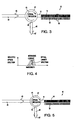
- the Bragg grating device 10 of the present invention is shown in conjunction with an optical circulator 42 for use as a variable weight tap.
- a variable weight tap may find particular usefulness in RF signal processors and arbitrary waveform generators.
- an optically modulated signal 43 enters into waveguide 44 from the left and enters the optical circulator 42.
- the signal travels clockwise from port to adjacent port as indicated on the optical circulator 42 (shown by the direction of the arrow 45) and enters into the waveguide 12 containing the Bragg grating device 10.
- the signal 43 continues along the waveguide 12 to the right. However, by injecting current into a portion of the grating structure 14, such as the portion 30, part of the optical signal 43 matching the refractive index of the activated portion 30 is reflected off of the activated portion 30 and travels back through the waveguide 12 to the optical circulator 42. After re-entering the optical circulator 42, the reflected signal 43 continues clockwise to the exit port 46 and travels along the waveguide 48.
- the time delay experienced by the reflected signal 43 may be controlled by appropriately selecting the portion of the Bragg grating structure 14 that is injected with current.
- the tap weight i.e., the amount of light that is reflected by the activated portion
- the tap weight may be controlled by adjusting the amount of current that is injected into the selected portion of the grating structure 14. That is, as illustrated in FIG. 4, because the optical frequency of the input signal 43 is constant, the tap weight is varied as the injected current increases the refractive index of the selected grating portion.
- changing the level of injected current moves the reflectivity spectrum of the activated portion in or out of the pass band.
- the wavelength of the reflected optical spectrum changes. This increase shifts the reflectivity spectrum to longer wavelengths.
- the optical carrier 12 which has a fixed optical wavelength, resonates or reflects from matched wavelengths different portions of the grating reflectivity spectrum and the amount of optical power that is reflected changes accordingly.
- FIG. 5 the device of FIG. 3 is reillustrated such that its use for generating a high precision true time delay may be described.
- an addressable, discrete, true time delay is effected on time scales impracticable through prior technology.
- a continuously variable true time delay is effected.
- different portions of the Bragg grating structure 14 can be shifted to different center wavelengths by injecting different current levels into each portion. This can provide the function of wavelength division multiplexed (WDM) true time delay.
- WDM wavelength division multiplexed
- the optically modulated signal 43 is input through the waveguide 44 and delivered to the optical circulator 42.
- the laser source for the optically modulated signal 43 preferably has a fixed frequency.
- the optical signal 43 travels through the waveguide 12 until the Bragg condition is met.
- ⁇ is the physical grating spacing
- the optical signal 43 is reflected and the round trip travel time is the desired true time delay.
- the reflected optical signal 43' re-enters the optical circulator 42 and exits the port 46 to travel along the waveguide 48.
- the time delay is in discreet steps defined by the positions of the electrodes along the length of the waveguide 12. If no discreet time step sizes are desired, then a combination of adjacent electrodes may be injected with current to effect a continuously variable time delay. This technique may find particular usefulness in creating the necessary time delay for a phased array antenna.
- a Bragg grating structure 14 on the order of 10 cm may be manufactured. Longer lengths are also possible by connecting 10 cm sections together with optical waveguides.
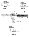
- any desired optical filter shape for use in either reflection or transmission applications can be made by specifically configuring the current injected portions of the Bragg grating structure 14. For example, by injecting two separate portions of the Bragg grating device 10, such as portions 30A and 30B, with two different levels of injection current, the two portions 30A and 30B are provided with two different effective indices of refraction, N 1 and N 2 . Similarly, by appropriately injecting current into various portions of the Bragg grating device 10 to a measured degree, the optical filter may be shaped to any desired filter function.
- a sinX/X function or other filter window function can provide filter shaping to reduce side lobes or optimize other filter characteristics.
- the optically modulated signal 43 entering into the waveguide 44 has a broad band optical spectrum such as that illustrated in FIG. 7.
- the optical signal 43 continues through the Bragg grating device 10.
- the optical spectrum of the signal transmitted through the Bragg grating device 10 i.e., continuing to the right in FIG. 6 and not returning to the optical circular 42
- the reflected signal 48 from the Bragg grating device 10 returns to the optical circular 42 and is ejected through the port 46 to the waveguide 48 with an optical spectrum such as that illustrated in FIG. 9.
- the Bragg grating device 10 can be provided with a chirp for the purpose of compensating for distortion of a modulated optical signal due to dispersion in an optical fiber used in long haul communications networks. This is accomplished by injecting slightly greater levels of current into consecutive portions of the Bragg grating structure 14 along the length of the Bragg grating device 10.
- the advantage here when compared to traditional, static, dispersion compensators, is that the Bragg grating device 10 can be modified to compensate for different long haul distances which have different amounts of distortion. It could further be optimally adjusted for a particular dispersion unique to a particular fiber type.
- the present invention may also be used as an optical spectrum analyzer to obtain the optical spectrum of an unknown signal by configuring the Bragg grating device 10 with a linear chirp.
- the injected current is varied linearly with distance along the Bragg grating structure 14.
- the input optical signal 43 is then gated on and off.
- the off time equals the round trip time delay to the end of the grating structure 14.
- the spectral components are output from the optical circulator 42 with short wavelengths exiting first and long wavelengths exiting last. Therefore, the time axis of the output spectral components corresponds to optical wavelength.
- the gradient of the chirp is tailored to the optical bandwidth of the input spectrum. One could then integrate a small or a large range of optical spectra.
- the present invention may also be used for complex taps by displacing the grating Bragg structure 14 in time and distance.
- a complex processor is constructed using the present invention by injecting current into a portion of the Bragg grating structure 14 which is located at a position that satisfies the amplitude adjustment of the reflected or transmitted waveform but also adjusts the waveform to the desired phase as measured against a reference phase or reference position in delay distance.
- the Bragg grating structure 14 is adjusted to its operative spacing by adjustment of the injected current. This may be accomplished over a distance of several adjacent electrodes if desired. For example, a first set of electrodes along the device 10 may be injected with current to adjust the reflection coefficient to a known value.
- a second set of electrodes of the same size as the first set but located downstream thereof could be injected with the same amount of current to obtain the same result in the amplitude component while shifting the phase of the reflected signal 43 relative to a time reference.
- a complex phasor may be implemented in the Bragg grating structure 14 which and may be combined with other structures to form complex signal processing on complex signals.
- the present invention may also be used to perform optical switching in the form of both signal routing and Time Division Multiple Access (TDMA) frame formatting.
- signal routing is implemented by controlling the travel direction of the optically modulated signal 43. If the Bragg grating structure 14 is made to be reflective then the reflected signal 43 is routed out through the time delayed output. Otherwise, the signal 43 passes through the Bragg grating structure 14 as a transmission. In this way, the non-switched signal 43 passes without being effected but the reflected signal 43 can be phased as described previously to fit within the timing requirements of a frame format as is found with TDMA communications standards. Additionally, all of these processes are effected while modifying the amplitude of the signal distribution.
- TDMA Time Division Multiple Access
- fractional power (A) can be routed straight through and (1-A) power can be phase adjusted and routed out the reflective port 46 of the circulator 42. This achieves not only routing of signals but the power allocation associated with their distribution as well.
- the present invention provides an addressable, adaptable, semiconductive Bragg grating device.
- the Bragg grating device enables a plurality of portions of a Bragg grating structure to be selectively injected with current such that the refractive index of each portion of the Bragg grating structure may be optimally controlled.
- the entire Bragg grating structure may be injected with current, none of the Bragg grating structure may be injected with current, an individual portion of the Bragg grating structure may be injected with current, or select combinations of individual portions of the Bragg grating structure may be injected with current.
- the amount of current injected into all, none, individual, or select combinations of the portions of the Bragg grating structure may be varied to effectuate further control of the reflected and transmitted optical signal.
- the device of the present invention will find usefulness in many different environments, it is presently believed to be particularly well suited for use in optical and RF spectrum analyzers, true time delays for phased array antennas and optical switches.
Landscapes
- Physics & Mathematics (AREA)
- Nonlinear Science (AREA)
- General Physics & Mathematics (AREA)
- Optics & Photonics (AREA)
- Optical Integrated Circuits (AREA)
- Optical Communication System (AREA)
- Optical Modulation, Optical Deflection, Nonlinear Optics, Optical Demodulation, Optical Logic Elements (AREA)
- Semiconductor Lasers (AREA)
Abstract
Description

Claims (14)
- An optical device comprising:an optical waveguide;a grating structure formed in said optical waveguide;a first plurality of electrodes disposed on said optical waveguide;a second plurality of electrodes disposed on said optical waveguide, said second plurality of electrodes being individually electrically coupled to said first plurality of electrodes through said grating structure; anda plurality of electrical leads coupled between said second plurality of electrodes and a power source.
- The device of claim 1 wherein said optical waveguide further comprises a semiconductive substrate.
- The device of claim 1 wherein said first and second plurality of electrodes further comprise individual electrodes disposed in an axially spaced relation along a length of said optical waveguide.
- The device of claim 1 wherein said first plurality of electrodes further comprise individual electrodes electrically isolated from one another.
- The device of claim 1 wherein said second plurality of electrodes further comprise individual electrodes electrically isolated from one another.
- The device of claim 5 wherein said electrodes of said second plurality of electrodes are discretely electrically coupled to individual electrodes of said first plurality of electrodes through said grating structure.
- The device of claim 5 wherein said plurality of electrical leads are selectively injectable with current such that select portions of said grating structure may be variably activated via said first and second plurality of electrodes.
- A Bragg grating device comprising:a semiconductive optical wave guide;a Bragg grating structure formed along a length of said optical wave guide;a first plurality of electrodes disposed on a first surface of said optical waveguide and communicating with select members at said Bragg grating structure;a second plurality of electrodes disposed on a second surface of said optical waveguide and communicating with said select members of said Bragg grating structure such that individual electrodes of said second plurality of electrodes are electrically coupled to individual electrodes of said first plurality of electrodes via said select members of said Bragg grating structure; anda plurality of electrical leads electrically coupled between said second plurality of electrodes and a power source such that a refractive index of discrete portions of said Bragg grating structure may be selectively varied.
- The Bragg grating device of Claim 8 further comprising a controller disposed between said plurality of electrical leads and said power source for varying a magnitude and distribution of power among said discrete portions of said Bragg grating structure.
- The Bragg grating device of Claim 8 wherein said semiconductive optical waveguide further comprises a double heterostructure InP/InGaAsP waveguide having said Bragg grating structure written over a core region thereof.
- The Bragg grating device of Claim 8 further comprising an antireflective coating disposed on said semiconductive optical waveguide.
- An addressable, adaptable, semiconductive, Bragg grating device comprising:a semiconductive optical waveguide having a preselected length;a Bragg grating structure etched into said waveguide along said length;a first plurality of electrodes disposed on a first surface of said waveguide and being equidistantly spaced apart along said length so as to be electrically isolated from one another, individual electrodes of said first plurality of electrodes being discretely coupled to separate members of said Bragg grating structure;a second plurality of electrodes disposed on a second surface of said waveguide opposite said first plurality of electrodes, said second plurality of electrodes being equidistantly spaced apart along said length so as to be electrically isolated from one another, individual electrodes of said second plurality of electrodes being discretely coupled to said separate members of said Bragg grating structure so as to communicate with said individual electrodes of said first plurality of electrodes to thereby define a plurality of discrete Bragg grating portions of said Bragg grating structure;a plurality of electrical leads electrically coupled to said second plurality of electrodes; anda controller coupled between said plurality of electrical leads and a power source to vary a magnitude and distribution of current among said plurality of discrete Bragg grating portions.
- The Bragg grating device of Claim 12 wherein said semiconductive optical waveguide further comprises a double heterostructure InP/InGaAsP waveguide having said Bragg grating structure written over a core region thereof.
- The Bragg grating device of Claim 12 further comprising an antireflective coating disposed on said semiconductive optical waveguide.
Applications Claiming Priority (2)
| Application Number | Priority Date | Filing Date | Title |
|---|---|---|---|
| US252497 | 1988-09-30 | ||
| US09/252,497 US6208773B1 (en) | 1999-02-18 | 1999-02-18 | Addressable, semiconductor adaptable Bragg gratings (ASABG) |
Publications (2)
| Publication Number | Publication Date |
|---|---|
| EP1030207A2 true EP1030207A2 (en) | 2000-08-23 |
| EP1030207A3 EP1030207A3 (en) | 2002-05-22 |
Family
ID=22956260
Family Applications (1)
| Application Number | Title | Priority Date | Filing Date |
|---|---|---|---|
| EP00101631A Withdrawn EP1030207A3 (en) | 1999-02-18 | 2000-01-31 | Addressable, semiconductor adaptable Bragg gratings |
Country Status (4)
| Country | Link |
|---|---|
| US (1) | US6208773B1 (en) |
| EP (1) | EP1030207A3 (en) |
| JP (1) | JP3434257B2 (en) |
| CA (1) | CA2298251C (en) |
Cited By (2)
| Publication number | Priority date | Publication date | Assignee | Title |
|---|---|---|---|---|
| FR2834082A1 (en) * | 2001-12-21 | 2003-06-27 | Thales Sa | DEVICE FOR MONITORING THE LAW OF SPECTRAL PULSE DISPERSION |
| WO2003077015A1 (en) * | 2002-03-14 | 2003-09-18 | Yissum Research Development Company Of The Hebrew University Of Jerusalem | Silicon light waveguide with mos capacitors positioned on the waveguide |
Families Citing this family (25)
| Publication number | Priority date | Publication date | Assignee | Title |
|---|---|---|---|---|
| US6563966B1 (en) * | 1999-03-04 | 2003-05-13 | Finisar Corporation, Inc. | Method, systems and apparatus for providing true time delayed signals using optical inputs |
| KR100351187B1 (en) * | 2000-11-07 | 2002-09-05 | 이호준 | an signal processing device of multi fiber bragg grating sensor using CDMA |
| US6947615B2 (en) | 2001-05-17 | 2005-09-20 | Sioptical, Inc. | Optical lens apparatus and associated method |
| US6748125B2 (en) | 2001-05-17 | 2004-06-08 | Sioptical, Inc. | Electronic semiconductor control of light in optical waveguide |
| CA2725883C (en) * | 2001-05-17 | 2013-11-19 | Sioptical, Inc. | Integrated optical waveguide device comprising a polysilicon layer-based passive optical waveguide device in combination with an active optical waveguide device, and method for making same |
| US6912330B2 (en) * | 2001-05-17 | 2005-06-28 | Sioptical Inc. | Integrated optical/electronic circuits and associated methods of simultaneous generation thereof |
| US6898352B2 (en) * | 2001-05-17 | 2005-05-24 | Sioptical, Inc. | Optical waveguide circuit including passive optical waveguide device combined with active optical waveguide device, and method for making same |
| US6690863B2 (en) | 2001-05-17 | 2004-02-10 | Si Optical, Inc. | Waveguide coupler and method for making same |
| US6738546B2 (en) * | 2001-05-17 | 2004-05-18 | Sioptical, Inc. | Optical waveguide circuit including multiple passive optical waveguide devices, and method of making same |
| US6646747B2 (en) | 2001-05-17 | 2003-11-11 | Sioptical, Inc. | Interferometer apparatus and associated method |
| US6842546B2 (en) * | 2001-05-17 | 2005-01-11 | Sioptical, Inc. | Polyloaded optical waveguide device in combination with optical coupler, and method for making same |
| US6891985B2 (en) * | 2001-05-17 | 2005-05-10 | Sioptical, Inc. | Polyloaded optical waveguide devices and methods for making same |
| US6891685B2 (en) * | 2001-05-17 | 2005-05-10 | Sioptical, Inc. | Anisotropic etching of optical components |
| US6625348B2 (en) | 2001-05-17 | 2003-09-23 | Optron X, Inc. | Programmable delay generator apparatus and associated method |
| US6654511B2 (en) | 2001-05-17 | 2003-11-25 | Sioptical, Inc. | Optical modulator apparatus and associated method |
| US6760498B2 (en) | 2001-05-17 | 2004-07-06 | Sioptical, Inc. | Arrayed waveguide grating, and method of making same |
| US6608945B2 (en) | 2001-05-17 | 2003-08-19 | Optronx, Inc. | Self-aligning modulator method and associated apparatus |
| US6658173B2 (en) | 2001-05-17 | 2003-12-02 | Optronx, Inc. | Interferometer and method of making same |
| US7496257B2 (en) | 2001-07-03 | 2009-02-24 | Brown University Research Foundation | Method and apparatus for detecting multiple optical wavelengths |
| CN1547677B (en) * | 2001-07-03 | 2012-05-23 | 布朗大学研究基金会 | Method and device for processing optical signal using super grating |
| EP1349242A1 (en) * | 2002-03-27 | 2003-10-01 | Alcatel | Raman fiber amplification stage; optical system and method to control the raman amplification stage |
| US7308161B2 (en) * | 2005-11-15 | 2007-12-11 | Massachusetts Institute Of Technology | System and method for wavelength selective switching employing single-element gratings |
| CN107735707B (en) * | 2015-03-20 | 2023-05-02 | 拉瓦尔大学 | Optical device and method for tuning an optical signal |
| CN107085319A (en) * | 2017-06-02 | 2017-08-22 | 天津理工大学 | Optical arbitrary pulse generator based on Bragg waveguide grating and its working method |
| CN114207462B (en) | 2019-07-10 | 2025-10-28 | 深圳市速腾聚创科技有限公司 | Optical antennas, optical phased array transmitters, and lidar systems |
Family Cites Families (7)
| Publication number | Priority date | Publication date | Assignee | Title |
|---|---|---|---|---|
| JPS5735828A (en) * | 1980-08-12 | 1982-02-26 | Matsushita Electric Ind Co Ltd | Integrated optical switch |
| CA2101411C (en) * | 1992-08-14 | 2003-06-10 | Jean-Pierre Weber | Tunable optical filter |
| SE470454B (en) * | 1992-08-26 | 1994-04-11 | Ericsson Telefon Ab L M | Optical filter device |
| KR100357787B1 (en) * | 1994-01-31 | 2003-01-24 | 가부시끼가이샤 히다치 세이사꾸쇼 | Manufacturing method of waveguide fluorescent element |
| JP3387746B2 (en) * | 1996-07-31 | 2003-03-17 | キヤノン株式会社 | Semiconductor laser capable of polarization modulation of bent channel stripe |
| US5982963A (en) * | 1997-12-15 | 1999-11-09 | University Of Southern California | Tunable nonlinearly chirped grating |
| JP2000235170A (en) | 1999-02-17 | 2000-08-29 | Nec Corp | Variable dispersion compensator |
-
1999
- 1999-02-18 US US09/252,497 patent/US6208773B1/en not_active Expired - Lifetime
-
2000
- 2000-01-31 EP EP00101631A patent/EP1030207A3/en not_active Withdrawn
- 2000-02-08 CA CA002298251A patent/CA2298251C/en not_active Expired - Fee Related
- 2000-02-16 JP JP2000037448A patent/JP3434257B2/en not_active Expired - Fee Related
Cited By (4)
| Publication number | Priority date | Publication date | Assignee | Title |
|---|---|---|---|---|
| FR2834082A1 (en) * | 2001-12-21 | 2003-06-27 | Thales Sa | DEVICE FOR MONITORING THE LAW OF SPECTRAL PULSE DISPERSION |
| WO2003054618A1 (en) * | 2001-12-21 | 2003-07-03 | Thales | Device for controlling pulse spectral dispersion law |
| WO2003077015A1 (en) * | 2002-03-14 | 2003-09-18 | Yissum Research Development Company Of The Hebrew University Of Jerusalem | Silicon light waveguide with mos capacitors positioned on the waveguide |
| US6987910B2 (en) | 2002-03-14 | 2006-01-17 | Yissum Research Development Company Of The Hebrew University Of Jerusalem | Silicon light waveguide with MOS capacitors positioned on the waveguide |
Also Published As
| Publication number | Publication date |
|---|---|
| CA2298251A1 (en) | 2000-08-18 |
| CA2298251C (en) | 2002-08-27 |
| US6208773B1 (en) | 2001-03-27 |
| EP1030207A3 (en) | 2002-05-22 |
| JP3434257B2 (en) | 2003-08-04 |
| JP2000241777A (en) | 2000-09-08 |
Similar Documents
| Publication | Publication Date | Title |
|---|---|---|
| US6208773B1 (en) | Addressable, semiconductor adaptable Bragg gratings (ASABG) | |
| US5022730A (en) | Wavelength tunable optical filter | |
| US4794346A (en) | Broadband semiconductor optical amplifier structure | |
| EP0665617B1 (en) | An alternating grating tunable DBR laser | |
| US5140651A (en) | Semiconductive guided-wave programmable optical delay lines using electrooptic fabry-perot elements | |
| EP1939653A2 (en) | Tunable resonant grating filters | |
| US4680769A (en) | Broadband laser amplifier structure | |
| IL103882A (en) | Monolithic integrated optical time delay network for antenna beam steering | |
| US7106922B2 (en) | Silicon-based tunable single passband optical filter | |
| US20040136415A1 (en) | Tunable semiconductor laser and method thereof | |
| US7006730B2 (en) | Multichannel integrated tunable thermo-optic lens and dispersion compensator | |
| JP2002299755A (en) | Fast and broadband tunable laser | |
| CN112468256A (en) | Chromatic dispersion and non-chromatic dispersion device cascade large-scale optical true time delay network based on wavelength division multiplexing | |
| EP1413021B1 (en) | Tuneable laser | |
| JPH1146046A (en) | Single mode laser | |
| US5978532A (en) | Spectrographic multiplexer component having an array of waveguides | |
| CN100593888C (en) | Single chip integrated semiconductor laser with tunable wavelength and without mode hopping | |
| US6999658B2 (en) | Optical resonator and laser applications | |
| He | Phase-dithered waveguide grating with flat passband and sharp transitions | |
| US5666374A (en) | Tunable optical arrangement | |
| US6023480A (en) | Fast tunable multiwavelength laser with folded imaging arrangement of nonoverlapping focal regions | |
| US5023885A (en) | External optical resonator for a semiconductor laser | |
| JPH0992933A (en) | Tunable semiconductor laser | |
| US20020186920A1 (en) | Coupler assisted tunable add/drop filter | |
| US6363093B1 (en) | Method and apparatus for a single-frequency laser |
Legal Events
| Date | Code | Title | Description |
|---|---|---|---|
| PUAI | Public reference made under article 153(3) epc to a published international application that has entered the european phase |
Free format text: ORIGINAL CODE: 0009012 |
|
| AK | Designated contracting states |
Kind code of ref document: A2 Designated state(s): AT BE CH CY DE DK ES FI FR GB GR IE IT LI LU MC NL PT SE |
|
| AX | Request for extension of the european patent |
Free format text: AL;LT;LV;MK;RO;SI |
|
| PUAL | Search report despatched |
Free format text: ORIGINAL CODE: 0009013 |
|
| AX | Request for extension of the european patent |
Free format text: AL;LT;LV;MK;RO;SI |
|
| RIC1 | Information provided on ipc code assigned before grant |
Free format text: 7G 02B 6/12 A, 7H 01S 5/12 B, 7H 01S 5/125 B, 7G 02B 5/18 B, 7G 02B 6/16 B |
|
| 17P | Request for examination filed |
Effective date: 20020712 |
|
| AKX | Designation fees paid |
Designated state(s): DE FR GB |
|
| 17Q | First examination report despatched |
Effective date: 20030325 |
|
| STAA | Information on the status of an ep patent application or granted ep patent |
Free format text: STATUS: THE APPLICATION IS DEEMED TO BE WITHDRAWN |
|
| 18D | Application deemed to be withdrawn |
Effective date: 20030805 |