EP1028564B1 - Estimation of carrier and sampling frequency offsets in multicarrier receivers - Google Patents
Estimation of carrier and sampling frequency offsets in multicarrier receivers Download PDFInfo
- Publication number
- EP1028564B1 EP1028564B1 EP99400319A EP99400319A EP1028564B1 EP 1028564 B1 EP1028564 B1 EP 1028564B1 EP 99400319 A EP99400319 A EP 99400319A EP 99400319 A EP99400319 A EP 99400319A EP 1028564 B1 EP1028564 B1 EP 1028564B1
- Authority
- EP
- European Patent Office
- Prior art keywords
- carrier
- frequency offset
- components
- module
- channel
- Prior art date
- Legal status (The legal status is an assumption and is not a legal conclusion. Google has not performed a legal analysis and makes no representation as to the accuracy of the status listed.)
- Expired - Lifetime
Links
- 238000005070 sampling Methods 0.000 title claims description 14
- 230000000694 effects Effects 0.000 claims description 6
- 230000003071 parasitic effect Effects 0.000 claims description 6
- 238000007476 Maximum Likelihood Methods 0.000 claims description 3
- 230000004044 response Effects 0.000 claims description 3
- 238000000034 method Methods 0.000 description 24
- 239000000969 carrier Substances 0.000 description 7
- 230000015556 catabolic process Effects 0.000 description 7
- 238000006731 degradation reaction Methods 0.000 description 7
- 238000012545 processing Methods 0.000 description 6
- 230000005540 biological transmission Effects 0.000 description 5
- 230000008901 benefit Effects 0.000 description 4
- 238000004891 communication Methods 0.000 description 3
- 238000010586 diagram Methods 0.000 description 3
- 230000009471 action Effects 0.000 description 2
- 238000003780 insertion Methods 0.000 description 2
- 230000037431 insertion Effects 0.000 description 2
- 230000007246 mechanism Effects 0.000 description 2
- 230000008569 process Effects 0.000 description 2
- 230000002040 relaxant effect Effects 0.000 description 2
- 101150012579 ADSL gene Proteins 0.000 description 1
- 102100020775 Adenylosuccinate lyase Human genes 0.000 description 1
- 108700040193 Adenylosuccinate lyases Proteins 0.000 description 1
- 239000000654 additive Substances 0.000 description 1
- 230000000996 additive effect Effects 0.000 description 1
- 230000032683 aging Effects 0.000 description 1
- 230000001427 coherent effect Effects 0.000 description 1
- 238000012937 correction Methods 0.000 description 1
- 239000013078 crystal Substances 0.000 description 1
- 230000007423 decrease Effects 0.000 description 1
- 238000005562 fading Methods 0.000 description 1
- 230000010363 phase shift Effects 0.000 description 1
- 238000011084 recovery Methods 0.000 description 1
- 238000004088 simulation Methods 0.000 description 1
- 238000012549 training Methods 0.000 description 1
Images


Classifications
-
- H—ELECTRICITY
- H04—ELECTRIC COMMUNICATION TECHNIQUE
- H04L—TRANSMISSION OF DIGITAL INFORMATION, e.g. TELEGRAPHIC COMMUNICATION
- H04L27/00—Modulated-carrier systems
- H04L27/26—Systems using multi-frequency codes
- H04L27/2601—Multicarrier modulation systems
- H04L27/2647—Arrangements specific to the receiver only
- H04L27/2655—Synchronisation arrangements
- H04L27/2662—Symbol synchronisation
-
- H—ELECTRICITY
- H04—ELECTRIC COMMUNICATION TECHNIQUE
- H04L—TRANSMISSION OF DIGITAL INFORMATION, e.g. TELEGRAPHIC COMMUNICATION
- H04L27/00—Modulated-carrier systems
- H04L27/26—Systems using multi-frequency codes
- H04L27/2601—Multicarrier modulation systems
- H04L27/2647—Arrangements specific to the receiver only
- H04L27/2655—Synchronisation arrangements
- H04L27/2657—Carrier synchronisation
-
- H—ELECTRICITY
- H04—ELECTRIC COMMUNICATION TECHNIQUE
- H04L—TRANSMISSION OF DIGITAL INFORMATION, e.g. TELEGRAPHIC COMMUNICATION
- H04L27/00—Modulated-carrier systems
- H04L27/26—Systems using multi-frequency codes
- H04L27/2601—Multicarrier modulation systems
- H04L27/2647—Arrangements specific to the receiver only
- H04L27/2655—Synchronisation arrangements
- H04L27/2668—Details of algorithms
- H04L27/2673—Details of algorithms characterised by synchronisation parameters
- H04L27/2676—Blind, i.e. without using known symbols
- H04L27/2679—Decision-aided
Definitions
- This invention relates to communication systems and particularly to those employing orthogonal frequency division multiplexing (OFDM) modulation methods.
- OFDM orthogonal frequency division multiplexing
- OFDM is a technique whereby information symbols are communicated from a transmitter to a receiver over a plurality of subcarriers.
- Carrier and clock frequency offsets can produce large degradations of the Bit Error Rate (BER) performance of Orthogonal Frequency Division Multiplex (OFDM) systems . See for example Proc. IEEE 83(6) 982-996 June 1995 and Proc. COST254 1997 . Indeed they not only produce extra-noise due to Inter Carrier Interference (ICI) but also a parasitic rotation of the symbols which also increases the BER.
- ICI Inter Carrier Interference
- carrier frequency offset means any difference in frequency between the carrier frequency generators in the transmitting and receiving circuitry and clock frequency offset means any difference between the sampling rates of the transmitting and receiving circuitry.
- a low-price ageing clock oscillator can have a frequency offset of 50 ppm (in fig.
- a sub-carrier is dedicated to clock recovery, which implies a loss of useful capacity of the system.
- the present invention comprises apparatus for blindly estimating carrier frequency offset and sampling frequency offset in accordance with claim 1.
- the invention thus provides a method and apparatus for jointly estimating carrier and clock frequency offsets on any channel, including frequency selective ones.
- the invention computes the estimates f ⁇ of f and ⁇ of e , by analyzing the rotations produced by clock and carrier frequency offsets on the received signals.
- the estimate f ⁇ can be added to that obtained with known algorithms, and may be used to compensate the carrier frequency offset on a time-domain signal.
- the estimate ⁇ can be used to steer the receiver clock frequency (e.g: using a Voltage Controlled Crystal Oscillator VCXO).
- VCXO Voltage Controlled Crystal Oscillator
- the invention can be used to advantage in the case of DAB because the method used is blind and can be easily applied on the differentially coded QPSK transmission.
- the invention can also be used as an alternative to the use of a dedicated channel.
- an OFDM transmitter comprises an Inverse Fast Fourier Transform modulator 1, a guard interval insertion block 2, a Parallel to Serial converter 3 a Digital to Analogue converter 4 and a mixer 5 having a local oscillator input f c .
- Information symbols S(k) are fed to the input of the modulator 1.
- the outputs from the modulator pass through block 2 where a guard interval is inserted. After guard interval insertion, the signals are fed to the Parallel-to- Serial converter 3 and then the resulting multiplexed output is fed to the Digital to Analogue converter 4.
- the resulting analogue signal is modulated onto a carrier of frequency fc by the action of the mixer 5 for transmission over a radio channel to the receiver of Fig.4
- the bandwidth is split among the N sub-carriers, so that the sub-carrier spacing is 1 NT .
- an OFDM receiver comprises a mixer 7 for converting the incoming signal on line 8 to baseband.
- a baseband signal at frequency fb,(nominally the carrier frequency) is supplied to the mixer 7 by a local oscillator 9.
- the baseband signal is then sampled in an Analogue to Digital converter 10 at a sampling rate fr (nominally the transmitter sampling rate, ft).
- the difference between the carrier frequency fc at the transmitter and the local oscillator frequency fb at the receiver is called the carrier frequency offset (fc-fb).
- f NT(fc-fb)
- the difference between the sampling frequency at the receiver and at the transmitter is called the clock frequency offset (fr-ft).
- the output signal from the Digital to Analogue converter 10 is fed to a Serial to Parallel converter 11.
- the resulting de-multiplexed outputs have the guard interval removed by the guard interval remover block 12 and then pass to a Discrete Fourier Transform demodulator 13.
- the outputs of the Discrete Fourier Transform demodulator 13 are subsequently passed through, in sequence, a Remove Channel Module 14, a Remove Modulation Module 15 and a Computation of Estimates Module 16.
- the outputs of the Computation Module 16 are the desired estimates of f and e .
- the demodulator 13 produces blocks of symbols Rm(k) at its outputs.
- the apparatus of Fig. 4 measures the phase drift due to carrier and clock frequency offsets between symbol (k-1) and symbol k. However, the phase has drifted continuously during the previous k-2, k-3, ... symbols because of carrier and clock frequency offsets and also because of the effects of the channel.
- the Remove Channel module 14 isolates the phase drift due to carrier, clock and channel between symbol (k-1) and symbol k.
- R m ( k ) R m ( k ) R m ( k -1).
- the output of the Module 15 is the block Z m ( k ) , where - K 2 ⁇ m ⁇ K 2 , m ⁇ 0.
- the rule can be the following:
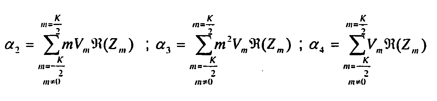
- a joint Maximum Likelihood Estimator (MLE) for ( f , ⁇ ) is computed from the observation Z m ( k ),where - K 2 ⁇ m ⁇ K 2 , m ⁇ 0.
- ⁇ and B ⁇ are proportional respectively to the desired f ⁇ and ⁇ .
- the estimation may be improved by using L blocks Z ( k 1 ), Z ( k 2 ),..., Z ( k L ) instead of just one block.
- the estimation may be improved by using L blocks Z ( k 1 ), Z ( k 2 ),..., Z ( k L ) instead of just one block.
- the total number of blocks chosen would depend upon the processing time available.
- coefficients V m can be replaced by 1. No loss of efficiency has been experienced in simulations.
- Figure 5 represents the processing architecture for realising the corresponding third processing step in which Vm is set to 1 (unity).
- Figs. 6 to 9 demonstrate the performance of the invention for the cases of two types of communication channel.
- the normalised channel frequency response in the first case is shown in Fig.6 .
- the second case relates to a typical DAB urban channel. 3, to take benefit from diversity effects.
- the clock frequency offset is below 20 ppm.
- the RMS of the clock frequency offset estimation error is shown in fig. 8
- the RMS of the carrier frequency offset estimation error in fig. 9 . Even in such poor conditions of transmission (fast varying channel), the method swiftly reaches the targeted performance .
Landscapes
- Engineering & Computer Science (AREA)
- Computer Networks & Wireless Communication (AREA)
- Signal Processing (AREA)
- Digital Transmission Methods That Use Modulated Carrier Waves (AREA)
- Synchronisation In Digital Transmission Systems (AREA)
- Cable Transmission Systems, Equalization Of Radio And Reduction Of Echo (AREA)
Description
- This invention relates to communication systems and particularly to those employing orthogonal frequency division multiplexing (OFDM) modulation methods.
- OFDM is a technique whereby information symbols are communicated from a transmitter to a receiver over a plurality of subcarriers.
- Carrier and clock frequency offsets can produce large degradations of the Bit Error Rate (BER) performance of Orthogonal Frequency Division Multiplex (OFDM) systems . See for example Proc. IEEE 83(6) 982-996 June 1995 and Proc. COST254 1997. Indeed they not only produce extra-noise due to Inter Carrier Interference (ICI) but also a parasitic rotation of the symbols which also increases the BER.
- Herein, carrier frequency offset means any difference in frequency between the carrier frequency generators in the transmitting and receiving circuitry and clock frequency offset means any difference between the sampling rates of the transmitting and receiving circuitry.
- There already exist several methods for estimating and compensating a carrier frequency offset. See for example,
US-A-5450456 (Mueller ) and Elec. Lett. 33(2) 113-114 Jan.1997. However, using either of these known methods, the residual carrier frequency offset can rise up to a few percent of the sub-carrier spacing and there still remains a degradation. As regards clock frequency offset, the degradation depends on the number of sub-carriers. If this number is large, this may prevent the designer from relaxing constraints on the receiver's clock generation mechanism. - To illustrate the problem, consider a typical OFDM transmission system such as Digital Audio Broadcasting (DAB)
mode 1. Infig. 1 and fig.2 , the degradation due to ICI is plotted. After correction with the classical algorithms, the carrier frequency offset can reach 3% of the sub-carrier spacing (infig. 2 , this corresponds to f= 3% where f is the carrier frequency offset expressed in number of sub-carrier spacings, N is the number of sub-carriers and T is the reciprocal of the sampling rate.) A low-price ageing clock oscillator can have a frequency offset of 50 ppm (infig. 1 , this corresponds to a normalised clock frequency offset e=5.105).Then at a Signal to Noise Ratio (SNR) of 20 dB, the ICI degradation can represent more than 1 dB. Moreover, the parasitic rotation due to f can represent 15% of the angle separating neighbour points of the QPSK (Quadrature Phase Shift Keying) constellation. The parasitic rotation due to e can represent 20% of this angle. Therefore, the error probability rises up severely. - Known methods which exist for reducing clock and carrier frequency offsets work on the assumption that time synchronization is achieved and that carrier frequency offset has been compensated up to a certain precision. However, there is still a need for a method with reduced complexity and better performance.
- In cable transmission , a sub-carrier is dedicated to clock recovery, which implies a loss of useful capacity of the system.
- In
US_A_5345440 (Gledhill ) a method is presented for estimating the carrier frequency offset and the clock offset. But only a formula for straight carrier frequency offset estimation is provided, whereas no formula for directly estimating the clock frequency offset is given. Besides, carrier and clock are estimated separately. Both phenomenona produce similar effects, so that a joint method for estimating both would have an improved efficiency and a reduced complexity. - In Elec. Lett. 34(6) 520-521 March 1998 , a method for jointly estimating carrier and clock frequency offsets is proposed. However, this method has the disadvantage of poor performance on a frequency-selective channel, such as the radio-mobile channel or cable channels.
- In
US_A_5802117 (Ghosh ), a joint method working on any channel is presented. However, it is not a 'blind' technique ie. It relies on a specific training signal. Therefore, it cannot be applied on any existing standardised communication system. - In a method for synchronization in OFDM modulation is disclosed in Patent Cooperation Treaty Patent Publication
WO95/19671 - There is subsequently a need for jointly and blindly estimating carrier and clock frequency offsets on any channel, including frequency selective ones and it is this need that the present invention addresses.
- Accordingly, the present invention comprises apparatus for blindly estimating carrier frequency offset and sampling frequency offset in accordance with
claim 1. - The invention thus provides a method and apparatus for jointly estimating carrier and clock frequency offsets on any channel, including frequency selective ones.
- The invention computes the estimates f̂ of f and ε̂ of e, by analyzing the rotations produced by clock and carrier frequency offsets on the received signals. The estimate f̂ can be added to that obtained with known algorithms, and may be used to compensate the carrier frequency offset on a time-domain signal. The estimate ε̂ can be used to steer the receiver clock frequency (e.g: using a Voltage Controlled Crystal Oscillator VCXO). Thus, the effect of carrier and clock frequency offsets is brought down to a negligible level, at the expense of slightly higher complexity.
- Advantages of the method compared with existing techniques are :
- The complexity required is low (a few times K, for a typical precision, where K is the number of useful sub-carriers).
- The implementation of the invention allows either to reduce the cost of the receiver by relaxing constraints on the clock oscillator and on the carrier synchronization mechanism, or to save power (the gain can then be greater than 1 dB)
- Since the method used is blind, it can be applied on existing standards such as ADSL, DAB or DVB-T. It works either on coherent or on differential modulation schemes;
- The method is flexible. The ability to track f and e depends on the number of symbols over which the estimation is performed. The more symbols, the more accurate and precise the estimate, but the lower the ability of tracking. Furthermore, the symbols picked up for the estimate do not need to be consecutive. For instance, in a time-varying channel, the chosen symbols can be spaced out. Thus, the complexity decreases and the estimation takes benefit from diversity effects. To summarize, it is easy to make a trade-off between complexity, performance and tracking.
- The invention can be used to advantage in the case of DAB because the method used is blind and can be easily applied on the differentially coded QPSK transmission.
- The invention can also be used as an alternative to the use of a dedicated channel.
- Some embodiments of the invention will now be described, by way of example only, with reference to the drawings of which :
-
Fig.1 is a graph showing number of sub-carriers v Signal-to-noise degradation due to ICI in an OFDM system having a relative clock frequency offset of 5.10exp(-5) ; -
Fig.2 is a graph showing carrier frequency offset v Signal-to-noise degradation in an OFDM system ; -
Fig.3 is a schematic block diagram of a conventional OFDM transmitter; -
Fig.4 is a schematic block diagram of an OFDM receiver incorporating carrier and clock frequency offset compensation means in accordance with the invention ; -
Fig.5 is a schematic block diagram illustrating the operation of the embodiment ofFig.4 in greater detail; -
Fig.6 is a graph showing sub-carrier index v normalised frequency response for a typical OFDM channel; -
Fig.7 is a graph showing number of symbols v RMS clock frequency offset estimation error for the OFDM channel operating in accordance with the invention ; -
Fig.8 is a graph showing number of symbols v RMS clock frequency offset estimation error for a DAB mode, OFDM channel operating in accordance with the invention ; and -
Fig.9 is a graph showing number of symbols v RMS carrier frequency offset estimation error for a DAB mode, OFDM channel operating in accordance with the invention. - With reference to
Fig.3 , an OFDM transmitter comprises an Inverse Fast FourierTransform modulator 1, a guardinterval insertion block 2, a Parallel to Serial converter 3 a Digital toAnalogue converter 4 and amixer 5 having a local oscillator input fc. Information symbols S(k) are fed to the input of themodulator 1. The outputs from the modulator pass throughblock 2 where a guard interval is inserted. After guard interval insertion, the signals are fed to the Parallel-to-Serial converter 3 and then the resulting multiplexed output is fed to the Digital toAnalogue converter 4. The Digital toAnalogue converter 4 has a sampling frequency ft = 1/T which is also the total bandwidth of the multiplexing process..The resulting analogue signal is modulated onto a carrier of frequency fc by the action of themixer 5 for transmission over a radio channel to the receiver ofFig.4 There are N sub-carriers with K useful sub-carriers. The bandwidth is split among the N sub-carriers, so that the sub-carrier spacing is
- Refering now to
Fig.4 , an OFDM receiver comprises amixer 7 for converting the incoming signal online 8 to baseband. A baseband signal at frequency fb,(nominally the carrier frequency) is supplied to themixer 7 by alocal oscillator 9. The baseband signal is then sampled in an Analogue toDigital converter 10 at a sampling rate fr (nominally the transmitter sampling rate, ft). - The difference between the carrier frequency fc at the transmitter and the local oscillator frequency fb at the receiver is called the carrier frequency offset (fc-fb). Expressed in terms of the number of sub-carrier spacings, f=NT(fc-fb) The difference between the sampling frequency at the receiver and at the transmitter is called the clock frequency offset (fr-ft). The relative (or normalised) clock frequency offset is denoted

- The output signal from the Digital to
Analogue converter 10 is fed to a Serial toParallel converter 11. The resulting de-multiplexed outputs have the guard interval removed by the guardinterval remover block 12 and then pass to a DiscreteFourier Transform demodulator 13. The outputs of the DiscreteFourier Transform demodulator 13 are subsequently passed through, in sequence, aRemove Channel Module 14, aRemove Modulation Module 15 and a Computation ofEstimates Module 16. The outputs of theComputation Module 16 are the desired estimates of f and e. - The
demodulator 13 produces blocks of symbols Rm(k) at its outputs. In order to generate the estimates of f and e, the apparatus ofFig. 4 measures the phase drift due to carrier and clock frequency offsets between symbol (k-1) and symbol k. However, the phase has drifted continuously during the previous k-2, k-3, ... symbols because of carrier and clock frequency offsets and also because of the effects of the channel. TheRemove Channel module 14 isolates the phase drift due to carrier, clock and channel between symbol (k-1) and symbol k. - Hence, at the output of the Discrete Fourier Transform (DFT)
demodulator 13, the k th block of symbols - Rm (k), where

Remove Channel Module 14. Here, the parasitic effects of the channel and of the rotation due to carrier and clock offset on block k - 1 are removed. At the output of theModule 14, the block of symbols Y m(k), where
Module 14 can consist either in differential demodulation or in equalization. For instance, in DAB, we have Ym (k) = Rm (k)Rm (k-1). A second processing step in theRemove Modulation Module 15 removes the "useful" rotation , due to modulation, from Ym (k) and also computes the quantity Vm = |Ym |. Thus there remains only the parasitic rotation produced by carrier and frequency offsets, in addition with various sources of perturbation (including thermal noise). The output of theModule 15 is the block Zm (k), where
- if (Ym (k)) > 0 and


- if (Ym (k)) < 0 and

-

- (Ym (k)) < 0 and


- if (Y m(k)) > 0 and


- But in the case of DAB, the rule can also be:| Zm (k)| = | Ym (k)|; arg(Z m(k)) = 4*arg(Ym (k))
- In a third step, a joint Maximum Likelihood Estimator (MLE) for (f,ε) is computed from the observation Zm (k),where

 is the real part of the associated element, and
 is the imaginary part of the associated element.
- It can be verified that, as long as


- Â and B̂ are proportional respectively to the desired f̂ and ε̂. The ratio depends on which method has been chosen for removing the modulation. For example, in DAB, if the first rule was applied, then :

- But if the second rule was appli ed, then:

- The MLE system of equations is derived as follows.
By the action of theRemove Channel Module 14 and theRemove Modulation Module 15, the vector
- This vector is approximated to the model:

- Vm (k) represents the modulus of the useful part of the signal,
- Vm (k) ≈ | Zm (k)| ≈ |Ym (k)| for high signal to noise ratio..
- γ : AWGN (Additive white Gaussian noise)
- It is desired to fit f and e so that the model best fits reality.
- Introducing vector


- From which equation (1) above is derived.
- In an alternative embodiment, the estimation may be improved by using L blocks Z(k 1), Z(k 2),..., Z(k L) instead of just one block.
- In this case, the coefficients to be computed for the estimate are the

- In an alternative embodiment, the estimation may be improved by using L blocks Z(k 1), Z(k 2),..., Z(kL ) instead of just one block.
- In this case, the coefficients to be computed for the estimate are the

- The total number of blocks chosen would depend upon the processing time available.
- The estimation may be performed on successive symbols kj = k1, k2,.....kL, with k2=k1+1, k3=k2+1 etc. However, when the channel variations are slow, the channel attenuation is almost the same on consecutive symbols. So, if channel fading worsens the estimate, using successive symbols will increase the complexity but not significantly improve the estimate. In this case then, the symbols chosen for the estimation can be spaced out, for instance choosing k2=k1+5, k3=k2+5...etc. The spacing chosen will depend on how fast the channel is varying.
- In a further alternative embodiment and in order to reduce the complexity of the process, coefficients V m can be replaced by 1. No loss of efficiency has been experienced in simulations.
Figure 5 represents the processing architecture for realising the corresponding third processing step in which Vm is set to 1 (unity). -
Figs. 6 to 9 demonstrate the performance of the invention for the cases of two types of communication channel. The normalised channel frequency response in the first case is shown inFig.6 . This corresponds to a baseband cable system.The second case relates to a typical DAB urban channel. 3, to take benefit from diversity effects. After 10 iterations, the clock frequency offset is below 20 ppm. The RMS of the clock frequency offset estimation error is shown infig. 8 , and the RMS of the carrier frequency offset estimation error infig. 9 . Even in such poor conditions of transmission (fast varying channel), the method swiftly reaches the targeted performance .
Claims (3)
- Apparatus for blindly estimating carrier frequency offset and sampling frequency offset between transmitter circuitry and receiver circuitry which communicate over a channel of an OFDM system, the apparatus including in a receiver circuit;
a local oscillator having a frequency fb for converting a received OFDM modulated signal s(t), representing information symbols S(k) having components Sm(k) sampled at a first sampling rate ft and modulated onto a carrier of frequency fc, to a base-band signal,
an analogue to digital converter having a second sampling rate fr for sampling the baseband signal,
a demodulator for performing a discrete Fourier transform on the sampled baseband signal to generate blocks of symbols R(k) having components Rm(k) representing the information symbols S(k) of components Sm(k),
characterized by the receiver circuit further including
a first module for removing parasitic effects of the channel on R(k) to generate at least one block Y(k) of components Ym(k),
a second module for removing modulation effects from Y(k) to generate at least one block Z(k) of components Zm(k) and to compute V of components Vm where Vm=/Ym /,
and a third module for calculating terms A and B relating respectively to the carrier frequency offset |fc-fb| and the sampling frequency offset |ft-fr| by performing a joint maximum likelihood estimation (MLE) solving the equations;

 is the real part of the associated element, and
 is the imaginary part of the associated element.
- Apparatus according to claim 1 in which said second module generates a plurality of blocks Z(k) and said third module adjusts coefficients of the MLE in response thereto.
- Apparatus according to claim 1 or claim 2 in which Vm is set to unity.
Priority Applications (5)
| Application Number | Priority Date | Filing Date | Title |
|---|---|---|---|
| DE69942222T DE69942222D1 (en) | 1999-02-11 | 1999-02-11 | Estimation of carrier and sampling frequency shifts in multi-carrier receivers |
| EP99400319A EP1028564B1 (en) | 1999-02-11 | 1999-02-11 | Estimation of carrier and sampling frequency offsets in multicarrier receivers |
| US09/496,302 US6198782B1 (en) | 1999-02-11 | 2000-02-01 | Estimation of frequency offsets in OFDM communication systems |
| CA002298722A CA2298722C (en) | 1999-02-11 | 2000-02-11 | Estimation of frequency offsets in ofdm communication systems |
| JP2000035081A JP4533492B2 (en) | 1999-02-11 | 2000-02-14 | Frequency offset estimation apparatus in OFDM communication system |
Applications Claiming Priority (1)
| Application Number | Priority Date | Filing Date | Title |
|---|---|---|---|
| EP99400319A EP1028564B1 (en) | 1999-02-11 | 1999-02-11 | Estimation of carrier and sampling frequency offsets in multicarrier receivers |
Publications (2)
| Publication Number | Publication Date |
|---|---|
| EP1028564A1 EP1028564A1 (en) | 2000-08-16 |
| EP1028564B1 true EP1028564B1 (en) | 2010-04-07 |
Family
ID=8241874
Family Applications (1)
| Application Number | Title | Priority Date | Filing Date |
|---|---|---|---|
| EP99400319A Expired - Lifetime EP1028564B1 (en) | 1999-02-11 | 1999-02-11 | Estimation of carrier and sampling frequency offsets in multicarrier receivers |
Country Status (5)
| Country | Link |
|---|---|
| US (1) | US6198782B1 (en) |
| EP (1) | EP1028564B1 (en) |
| JP (1) | JP4533492B2 (en) |
| CA (1) | CA2298722C (en) |
| DE (1) | DE69942222D1 (en) |
Families Citing this family (28)
| Publication number | Priority date | Publication date | Assignee | Title |
|---|---|---|---|---|
| US6442221B1 (en) * | 1998-09-22 | 2002-08-27 | Zenith Electronics Corporation | Ghost eliminating equalizer |
| WO2000033496A1 (en) * | 1998-12-01 | 2000-06-08 | Samsung Electronics Co., Ltd. | Frequency synchronizing device for ofdm/cdma system |
| US6891792B1 (en) * | 1999-05-14 | 2005-05-10 | At&T Corp. | Method for estimating time and frequency offset in an OFDM system |
| US20020065047A1 (en) * | 2000-11-30 | 2002-05-30 | Moose Paul H. | Synchronization, channel estimation and pilot tone tracking system |
| US7012881B2 (en) * | 2000-12-29 | 2006-03-14 | Samsung Electronic Co., Ltd. | Timing and frequency offset estimation scheme for OFDM systems by using an analytic tone |
| NZ509688A (en) * | 2001-02-01 | 2003-06-30 | Ind Res Ltd | Maximum likelihood sychronisation (estimating time delay) for wireless digital communications system using a pilot symbol |
| US20020172183A1 (en) * | 2001-05-17 | 2002-11-21 | Josef Eichinger | Method and device for transmitting data in radio channels with strong multipath propagation and increased data volume in a radio communication system |
| KR20040008204A (en) * | 2001-05-31 | 2004-01-28 | 노오텔 네트웍스 리미티드 | Apparatus and method for measuring sub-carrier frequencies and sub-carrier frequency offsets |
| US7962162B2 (en) * | 2001-08-07 | 2011-06-14 | At&T Intellectual Property Ii, L.P. | Simulcasting OFDM system having mobile station location identification |
| US7020222B2 (en) * | 2001-10-24 | 2006-03-28 | Texas Instruments Incorporated | Efficient method and system for offset phasor determination |
| US7324606B2 (en) * | 2001-10-31 | 2008-01-29 | Henry Stephen Eilts | Computationally efficient system and method for channel estimation |
| US7209433B2 (en) * | 2002-01-07 | 2007-04-24 | Hitachi, Ltd. | Channel estimation and compensation techniques for use in frequency division multiplexed systems |
| US7346135B1 (en) | 2002-02-13 | 2008-03-18 | Marvell International, Ltd. | Compensation for residual frequency offset, phase noise and sampling phase offset in wireless networks |
| SG102042A1 (en) * | 2002-04-03 | 2004-02-27 | Sony Electronics Singapore Pte | Methods and apparatus for receiving ofdm signals |
| KR100478148B1 (en) * | 2002-05-31 | 2005-03-21 | 한국과학기술원 | Carrier frequency estimation method for transmissions with antenna diversity |
| US7173991B2 (en) | 2002-06-17 | 2007-02-06 | Hitachi, Ltd. | Methods and apparatus for spectral filtering channel estimates |
| US7139340B2 (en) * | 2002-06-28 | 2006-11-21 | Hitachi, Ltd. | Robust OFDM carrier recovery methods and apparatus |
| KR100553544B1 (en) * | 2002-08-31 | 2006-02-20 | 삼성탈레스 주식회사 | Frequency Offset Estimation and Channel Equalization in Burst Orthogonal Frequency Division Multiplexing Systems |
| KR100488802B1 (en) | 2002-12-09 | 2005-05-12 | 한국전자통신연구원 | Method and apparatus for carrier frequency offset and sampling clock frequency offset tracking in orthogonal frequency division multiplexing wireless communication systems |
| US7433435B2 (en) * | 2003-10-22 | 2008-10-07 | Sasken Communication Technologies Limited | Apparatus, methods, systems, and articles incorporating a clock correction technique |
| KR100538775B1 (en) * | 2004-04-09 | 2005-12-23 | 전자부품연구원 | Method and apparatus for intelligent channel selection against various interferers in wireless communication systems and receiver using intelligent channel selection |
| KR100606113B1 (en) * | 2004-07-22 | 2006-07-28 | 삼성전자주식회사 | Maximum Frequency Offset Estimation Method for Mobile Communication Systems in Fast Rayleigh Fading Channel Environment |
| KR100752641B1 (en) * | 2005-01-25 | 2007-08-29 | 삼성전자주식회사 | ODF signal receiver and method for estimating common phase using data subcarrier |
| DE102005007072B4 (en) * | 2005-02-16 | 2010-07-22 | Rohde & Schwarz Gmbh & Co. Kg | Method for synchronizing a measuring signal with a reference signal and corresponding measuring system |
| US20080107098A1 (en) * | 2006-11-08 | 2008-05-08 | Paul Spencer | Multislot-mode automatic frequency correction apparatus, systems, and methods |
| WO2008082367A1 (en) * | 2007-01-05 | 2008-07-10 | Agency For Science, Technology And Research | A method of determining a carrier frequency offset between a transmitter and a receiver |
| CN101237436B (en) * | 2007-01-31 | 2011-03-23 | 扬智科技股份有限公司 | A method and circuit for detecting carrier frequency offset and sampling frequency offset |
| US10243682B2 (en) * | 2016-08-22 | 2019-03-26 | Phasorlab, Inc. | Time-domain and frequency-domain approach to frequency offset correction method for LTE SC-FDMA uplink |
Family Cites Families (10)
| Publication number | Priority date | Publication date | Assignee | Title |
|---|---|---|---|---|
| JPS59149440A (en) * | 1983-02-16 | 1984-08-27 | Nec Corp | Offset suppression type control system for carrier timing coupling |
| GB9020170D0 (en) | 1990-09-14 | 1990-10-24 | Indep Broadcasting Authority | Orthogonal frequency division multiplexing |
| US5206886A (en) * | 1990-04-16 | 1993-04-27 | Telebit Corporation | Method and apparatus for correcting for clock and carrier frequency offset, and phase jitter in mulicarrier modems |
| US5206884A (en) * | 1990-10-25 | 1993-04-27 | Comsat | Transform domain quantization technique for adaptive predictive coding |
| US5450456A (en) | 1993-11-12 | 1995-09-12 | Daimler Benz Ag | Method and arrangement for measuring the carrier frequency deviation in a multi-channel transmission system |
| SE9400116L (en) * | 1994-01-18 | 1995-03-27 | Telia Ab | Procedure and arrangement for synchronization in OFDM modulation |
| AU687228B2 (en) * | 1994-07-29 | 1998-02-19 | Qualcomm Incorporated | Method and apparatus for performing code acquisition in a CDMA communications system |
| US5802117A (en) | 1996-02-08 | 1998-09-01 | Philips Electronics North America Corporation | Method and apparatus for joint frequency offset and timing estimation of a multicarrier modulation system |
| US5732113A (en) * | 1996-06-20 | 1998-03-24 | Stanford University | Timing and frequency synchronization of OFDM signals |
| FR2756687B1 (en) * | 1996-11-29 | 2001-10-05 | Daewoo Electronics Co Ltd | DEVICE FOR CORRECTING A FREQUENCY OFFSET IN AN OFDM RECEPTION SYSTEM |
-
1999
- 1999-02-11 DE DE69942222T patent/DE69942222D1/en not_active Expired - Lifetime
- 1999-02-11 EP EP99400319A patent/EP1028564B1/en not_active Expired - Lifetime
-
2000
- 2000-02-01 US US09/496,302 patent/US6198782B1/en not_active Expired - Lifetime
- 2000-02-11 CA CA002298722A patent/CA2298722C/en not_active Expired - Lifetime
- 2000-02-14 JP JP2000035081A patent/JP4533492B2/en not_active Expired - Fee Related
Also Published As
| Publication number | Publication date |
|---|---|
| CA2298722C (en) | 2008-04-01 |
| JP4533492B2 (en) | 2010-09-01 |
| CA2298722A1 (en) | 2000-08-11 |
| US6198782B1 (en) | 2001-03-06 |
| EP1028564A1 (en) | 2000-08-16 |
| DE69942222D1 (en) | 2010-05-20 |
| JP2000244448A (en) | 2000-09-08 |
Similar Documents
| Publication | Publication Date | Title |
|---|---|---|
| EP1028564B1 (en) | Estimation of carrier and sampling frequency offsets in multicarrier receivers | |
| US7139321B2 (en) | Channel estimation for wireless OFDM systems | |
| US7469106B2 (en) | Reference phase and amplitude estimation for coherent optical receiver | |
| US8014472B1 (en) | Integer frequency offset estimation in wireless systems | |
| US6546055B1 (en) | Carrier offset determination for RF signals having a cyclic prefix | |
| US7539125B2 (en) | Method and circuit for frequency offset estimation in frequency domain in the orthogonal frequency division multiplexing baseband receiver for IEEE 802.11A/G wireless LAN standard | |
| RU2479131C2 (en) | Signal processing device, signal processing method and receiving system | |
| US7684501B2 (en) | Apparatus and method for carrier frequency offset and phase compensation in communication system | |
| US7639733B1 (en) | Maximum likelihood estimation of time and frequency offset for OFDM systems | |
| US9306789B2 (en) | Estimation of CFO based on relative values of frequency bins corresponding to used subcarriers of received preamble symbols for OFDM systems | |
| US7333548B2 (en) | Phase and frequency drift compensation in Orthogonal Frequency Division Multiplexing systems | |
| JP3429746B2 (en) | Echo phase offset correction in multicarrier demodulation systems | |
| US20080232496A1 (en) | Device and method for compensating timing offset | |
| US6961393B1 (en) | In-band-on-channel (IBOC) system and methods of operation using orthogonal frequency division multiplexing (OFDM) with timing and frequency offset correction | |
| US7526020B2 (en) | Circuit for improving channel impulse response estimation and compensating for remnant frequency offset in the orthogonal frequency division multiplexing (OFDM) baseband receiver for IEEE 802.11a/g wireless LAN standard | |
| JP4526662B2 (en) | Data transmission method and receiver | |
| US9363125B2 (en) | Blind phase tracking method for a filter bank multi-carrier (FBMC)receiver | |
| KR20020056986A (en) | Modulator and demodulator using dispersed pilot subchannel and ofdm frame structure in orthogonal frequency division multiplexing system | |
| US20020085651A1 (en) | Removing frequency and timing offsets in digital transmitters and receivers | |
| WO2010072677A1 (en) | Method and apparatus for estimating phase noise in an ofdm transmission system | |
| WO2008069556A1 (en) | Amplitude-differential phase shift keying modulation apparatus and method | |
| EP2202906B1 (en) | Data-aided signal-to-noise ratio estimate for M-DPSK modulation systems with division of the received samples into blocks | |
| US7515657B1 (en) | Frequency tracking for OFDM transmission over frequency selective channels | |
| US8223865B2 (en) | Method for the blind estimation of OFDM signal parameters by adapted filtering | |
| JP2001044963A (en) | Receiver |
Legal Events
| Date | Code | Title | Description |
|---|---|---|---|
| PUAI | Public reference made under article 153(3) epc to a published international application that has entered the european phase |
Free format text: ORIGINAL CODE: 0009012 |
|
| AK | Designated contracting states |
Kind code of ref document: A1 Designated state(s): DE ES FR GB IT NL |
|
| AX | Request for extension of the european patent |
Free format text: AL;LT;LV;MK;RO;SI |
|
| 17P | Request for examination filed |
Effective date: 20000923 |
|
| AKX | Designation fees paid |
Free format text: DE ES FR GB IT NL |
|
| 17Q | First examination report despatched |
Effective date: 20061222 |
|
| GRAP | Despatch of communication of intention to grant a patent |
Free format text: ORIGINAL CODE: EPIDOSNIGR1 |
|
| GRAS | Grant fee paid |
Free format text: ORIGINAL CODE: EPIDOSNIGR3 |
|
| GRAA | (expected) grant |
Free format text: ORIGINAL CODE: 0009210 |
|
| AK | Designated contracting states |
Kind code of ref document: B1 Designated state(s): DE ES FR GB IT NL |
|
| REG | Reference to a national code |
Ref country code: GB Ref legal event code: FG4D |
|
| REF | Corresponds to: |
Ref document number: 69942222 Country of ref document: DE Date of ref document: 20100520 Kind code of ref document: P |
|
| REG | Reference to a national code |
Ref country code: NL Ref legal event code: VDEP Effective date: 20100407 |
|
| PG25 | Lapsed in a contracting state [announced via postgrant information from national office to epo] |
Ref country code: NL Free format text: LAPSE BECAUSE OF FAILURE TO SUBMIT A TRANSLATION OF THE DESCRIPTION OR TO PAY THE FEE WITHIN THE PRESCRIBED TIME-LIMIT Effective date: 20100407 Ref country code: ES Free format text: LAPSE BECAUSE OF FAILURE TO SUBMIT A TRANSLATION OF THE DESCRIPTION OR TO PAY THE FEE WITHIN THE PRESCRIBED TIME-LIMIT Effective date: 20100718 |
|
| PLBE | No opposition filed within time limit |
Free format text: ORIGINAL CODE: 0009261 |
|
| STAA | Information on the status of an ep patent application or granted ep patent |
Free format text: STATUS: NO OPPOSITION FILED WITHIN TIME LIMIT |
|
| REG | Reference to a national code |
Ref country code: GB Ref legal event code: 732E Free format text: REGISTERED BETWEEN 20110127 AND 20110202 |
|
| 26N | No opposition filed |
Effective date: 20110110 |
|
| PG25 | Lapsed in a contracting state [announced via postgrant information from national office to epo] |
Ref country code: IT Free format text: LAPSE BECAUSE OF FAILURE TO SUBMIT A TRANSLATION OF THE DESCRIPTION OR TO PAY THE FEE WITHIN THE PRESCRIBED TIME-LIMIT Effective date: 20100407 |
|
| REG | Reference to a national code |
Ref country code: DE Ref legal event code: R081 Ref document number: 69942222 Country of ref document: DE Owner name: MOTOROLA MOBILITY, INC. ( N.D. GES. D. STAATES, US Free format text: FORMER OWNER: MOTOROLA, INC., SCHAUMBURG, US Effective date: 20110324 Ref country code: DE Ref legal event code: R081 Ref document number: 69942222 Country of ref document: DE Owner name: MOTOROLA MOBILITY, INC. ( N.D. GES. D. STAATES, US Free format text: FORMER OWNER: MOTOROLA, INC., SCHAUMBURG, ILL., US Effective date: 20110324 |
|
| REG | Reference to a national code |
Ref country code: FR Ref legal event code: TP Owner name: MOTOROLA MOBILITY, INC., US Effective date: 20110912 |
|
| REG | Reference to a national code |
Ref country code: FR Ref legal event code: PLFP Year of fee payment: 18 |
|
| PGFP | Annual fee paid to national office [announced via postgrant information from national office to epo] |
Ref country code: DE Payment date: 20160226 Year of fee payment: 18 |
|
| REG | Reference to a national code |
Ref country code: FR Ref legal event code: PLFP Year of fee payment: 19 |
|
| PGFP | Annual fee paid to national office [announced via postgrant information from national office to epo] |
Ref country code: FR Payment date: 20170223 Year of fee payment: 19 |
|
| PGFP | Annual fee paid to national office [announced via postgrant information from national office to epo] |
Ref country code: GB Payment date: 20170227 Year of fee payment: 19 |
|
| REG | Reference to a national code |
Ref country code: DE Ref legal event code: R119 Ref document number: 69942222 Country of ref document: DE |
|
| REG | Reference to a national code |
Ref country code: GB Ref legal event code: 732E Free format text: REGISTERED BETWEEN 20170831 AND 20170906 |
|
| REG | Reference to a national code |
Ref country code: FR Ref legal event code: TP Owner name: GOOGLE TECHNOLOGY HOLDINGS LLC, US Effective date: 20171214 Ref country code: FR Ref legal event code: CD Owner name: GOOGLE TECHNOLOGY HOLDINGS LLC, US Effective date: 20171214 |
|
| PG25 | Lapsed in a contracting state [announced via postgrant information from national office to epo] |
Ref country code: DE Free format text: LAPSE BECAUSE OF NON-PAYMENT OF DUE FEES Effective date: 20170901 |
|
| GBPC | Gb: european patent ceased through non-payment of renewal fee |
Effective date: 20180211 |
|
| REG | Reference to a national code |
Ref country code: FR Ref legal event code: ST Effective date: 20181031 |
|
| PG25 | Lapsed in a contracting state [announced via postgrant information from national office to epo] |
Ref country code: GB Free format text: LAPSE BECAUSE OF NON-PAYMENT OF DUE FEES Effective date: 20180211 Ref country code: FR Free format text: LAPSE BECAUSE OF NON-PAYMENT OF DUE FEES Effective date: 20180228 |
|
| P01 | Opt-out of the competence of the unified patent court (upc) registered |
Effective date: 20230511 |