EP1026821A2 - Radio frequency modulator having isolation switches and signal path bypassing amplifier and modulator - Google Patents
Radio frequency modulator having isolation switches and signal path bypassing amplifier and modulator Download PDFInfo
- Publication number
- EP1026821A2 EP1026821A2 EP00300751A EP00300751A EP1026821A2 EP 1026821 A2 EP1026821 A2 EP 1026821A2 EP 00300751 A EP00300751 A EP 00300751A EP 00300751 A EP00300751 A EP 00300751A EP 1026821 A2 EP1026821 A2 EP 1026821A2
- Authority
- EP
- European Patent Office
- Prior art keywords
- switch
- modulator
- signal
- amplifier
- antenna
- Prior art date
- Legal status (The legal status is an assumption and is not a legal conclusion. Google has not performed a legal analysis and makes no representation as to the accuracy of the status listed.)
- Ceased
Links
Images







Classifications
-
- H—ELECTRICITY
- H04—ELECTRIC COMMUNICATION TECHNIQUE
- H04N—PICTORIAL COMMUNICATION, e.g. TELEVISION
- H04N5/00—Details of television systems
- H04N5/76—Television signal recording
- H04N5/765—Interface circuits between an apparatus for recording and another apparatus
- H04N5/775—Interface circuits between an apparatus for recording and another apparatus between a recording apparatus and a television receiver
- H04N5/7755—Interface circuits between an apparatus for recording and another apparatus between a recording apparatus and a television receiver the recorder being connected to, or coupled with, the antenna of the television receiver
-
- H—ELECTRICITY
- H04—ELECTRIC COMMUNICATION TECHNIQUE
- H04N—PICTORIAL COMMUNICATION, e.g. TELEVISION
- H04N5/00—Details of television systems
- H04N5/44—Receiver circuitry for the reception of television signals according to analogue transmission standards
Definitions
- the present invention relates to a radio frequency (RF) modulator.
- the RF modulator according to the present invention may be used, for example, in video tape recorders, satellite broadcasting receivers, and the like.
- Fig. 6 Conventionally, the construction of Fig. 6 is known as an RF modulator for use in the PAL (Phase Alternation by Line) color television system or the SECAM (séquential 07 á code) system.
- the antenna input terminal 1 is an input terminal, which is to be connected to an antenna, for receiving a television signal.
- the tuner output terminal 3 is to be connected with a tuner unit, for supplying a received television signal to the tuner unit.
- the tuner unit is installed in a video tape recorder.
- the antenna output terminal 2 is to be connected with an antenna terminal of an external television receiver, for outputting an amplified television signal, or a modulated signal.
- the amplified television signal is generated by amplifying by the amplifier 7 the television signal received through the antenna output terminal 2.
- the modulated signal is generated by the modulator 4 based on the video and audio signals respectively received through the video input terminal 5 and the audio input terminal 6.
- the modulated signal has a predetermined channel frequency.
- the video input terminal 5 is to be connected with a video output terminal of the video tape recorder, for inputting the video signal
- the audio input terminal 6 is to be connected with an audio output terminal of the video tape recorder, for inputting the audio signal.
- the television signal received through the antenna input terminal 1 is amplified by the amplifier 7, and is then distributed by the distributor 9 to the tuner output terminal 3 and the antenna output terminal 2.
- the signal distributed to the antenna output terminal 2 is amplified by the amplifier 8, and input into the mixer 10.
- the amplifier 8 may be dispensed with.
- the video signal and the audio signal which are input from the video input terminal 5 and the audio input terminal 6 are converted by the modulator 4 to a high-frequency modulated signal, and input into the mixer 10.
- the mixer 10 is connected with the antenna output terminal 2 to output the modulated signal or the amplified television signal.
- the path from the antenna input terminal 1 to the antenna output terminal 2 must be kept active for the television signal, so that the television signal can be displayed on the external television receiver. That is, the amplifiers 7 and 8 must be kept active even in the stand-by time of the video tape recorder, and therefore power consumption is increased.
- Japanese Unexamined Utility Model Application No. 2-111946 discloses a technique as illustrated in Fig. 7.
- a switch 15 is connected in parallel with the amplifiers 7 and 8 between the antenna input terminal 1 and the antenna output terminal 2.
- the switch 15 is controlled to be off when the amplifiers 7 and 8 are activated, and to be on when the amplifiers 7 and 8 are inactivated.
- the television signal can pass through the construction of Fig. 7 from the antenna input terminal 1 to the antenna output terminal 2 even when an electric power is not supplied to the construction of Fig. 7.
- An object of the present invention is to provide a radio frequency (RF) modulator in which power consumption and signal loss during the stand-by time of the video tape recorder are reduced.
- RF radio frequency
- a radio frequency modulator containing a modulator which converts an input video signal and an input audio signal into a modulated signal having a predetermined channel frequency; an amplifier amplifying an input signal from an antenna input terminal; a mixer which mixes the modulated signal with the input signal amplified by the amplifier to output a mixed signal from an antenna output terminal; a first switch connected in parallel with the amplifier between the antenna input terminal and the antenna output terminal; a second switch connected between the antenna input terminal and the amplifier; and a third switch connected between the mixer and the antenna output terminal.
- the second switch may be controlled to be on when the amplifier is activated, and the second switch may be controlled to be off when the amplifier is inactivated.
- the second switch may be controlled to be off when the amplifier is inactivated.
- the third switch may be controlled to be on when the modulator or the amplifier is activated, and the third switch may be controlled to be off when both of the modulator and the amplifier are inactivated.
- the first switch may be controlled to be off when the third switch is on, and the first switch may be controlled to be on when the third switch is off.
- the first switch may be controlled to be on when the third switch is off.
- the first switch may contain a switch circuit using a plurality of field effect transistors, and a transistor which is connected between at least two field effect transistors among the plurality of field effect transistors.
- the transistor grounds a signal leaked from the modulator when the at least two field effect transistors are in an unconductive state. Thus, signal loss can be further suppressed.
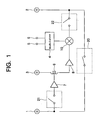
- Fig. 1 is a diagram illustrating the entire construction of the first embodiment of the present invention.
- the first switch 20 is connected in parallel with the amplifiers 7 and 8 between the antenna input terminal 1 and the antenna output terminal 2
- the second switch 21 is connected between the antenna input terminal 1 and the amplifier 7
- the third switch 22 is connected between the mixer 10 and the antenna output terminal 2.
- the first switch 20 When the amplifiers 7 and 8 are activated, the first switch 20 is turned off, and the second and third switches 21 and 22 are turned on, the signal received through the antenna input terminal 1 is output through the amplifiers 7 and 8 from the antenna output terminal 2.
- the first switch 20 When the amplifiers 7 and 8 are inactivated, the first switch 20 is turned on, and the second and third switches 21 and 22 are turned off, the signal received through the antenna input terminal 1 is output through the first switch 20 from the antenna output terminal 2. In this case, the received signal can reach the antenna output terminal 2 without influence of the amplifiers 7 and 8 and the mixer 10.
- the above first, second and third switches 20, 21, and 22 may be realized by mechanical switches as illustrated in Fig. 2, which shows the states of the mechanical switches when the amplifiers 7 and 8 are activated.
- Fig. 3 shows a construction of a switch circuit which is used as each of the second and third switches 21 and 22 in the third embodiment of the present invention.
- a certain voltage is applied to a power supply terminal 36
- a current flows through the resistor 32, the switching diode 31, and the resistor 33.
- the internal resistance of the switching diode 31 decreases when a current flows therethrough. Therefore, when a certain voltage is applied to the power supply terminal 36, a signal can pass through the switching diode 31, i.e., the switch of Fig. 3 is turned on.
- the switch of Fig. 3 When a certain voltage is not applied to the power supply terminal 36, no current flows through the switching diode 31, the internal resistance of the switching diode 31 increases, and therefore the switch of Fig.
- the capacitors 34 and 35 are DC blocking capacitors provided for preventing a flow of the switch control current into the antenna input terminal 1 or the antenna output terminal 2.
- Fig. 4 shows the construction of an FET switch circuit which is used as the first switch 20 in the fourth embodiment of the present invention.
- the FET (field effect transistor) 41 is an n-channel FET performing a switching action. When no voltage is applied to the power supply terminal 47, the gate and the source of the FET 41 are at the same potential, and therefore a current flows between the source and the drain of the FET 41, i.e., the FET 41 is turned on.
- the capacitors 45 and 46 are the DC blocking capacitors.
- Fig. 1 when the modulator 4 is activated, the third switch 22 is on, and the first switch 20 is off. If the first switch is an electronic switch, and the electronic switch does not achieve sufficient insulation, a portion of the output of the modulator 4 may leak through the first switch 20 to the antenna input terminal 1. In order to prevent such leakage, it is possible to lift the insulation level by providing more than one first switch, or connecting one or more transistors in the channel.
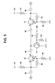
- the construction of Fig. 5 is one example of such provision.
- Fig. 5 is a diagram illustrating the construction of the switch circuit in the fifth embodiment of the present invention.
- the FETs 41 and 51 in Fig. 5 each have the same function as the FET 41 in Fig. 4, the resistors 42 and 52 in Fig. 5 have the same function as the resistor 42 in Fig. 4, the resistors 43 and 53 in Fig. 5 have the same function as the resistor 43 in Fig. 4, the resistors 44 and 54 in Fig. 5 each have the same function as the resistor 44 in Fig. 4, the capacitors 45, 46, 55, and 56 each have the same function as the capacitors 45 and 46 in Fig. 4, and the power supply terminals 47 and 57 each have the same function as the power supply terminal 47 in Fig. 4.
- an NPN transistor 61 is connected to a path between the FETs 41 and 51, and the resistors 62 and 63 are connected to the base of the transistor 61.
- the resistor 62 is a protection resistor, and one end of the resistors 62 is another power supply terminal 64.
- the resistor 63 is provided so that the potentials of the base and the emitter of the transistor 61 become the same level when no voltage is applied to the power supply terminal 64.
- the potentials of the base and the emitter of the transistor 61 are the same level due to the provision of the resistor 63, the collector and the emitter become open, and therefore the transistor 61 does not influence the signal path between the FETs 41 and 51.
- the potential of the base of the transistor 61 becomes higher than the potential of the emitter, and therefore a current flows from the collector to the emitter of the transistor 61, i.e., the transistor 61 is turned on. Therefore, it is possible to ground the signal leaked from the modulator 4 when the FETs 41 and 51 are in an unconductive state for blocking signals. Thus, the insulation level can be lifted.
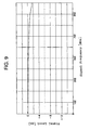
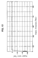
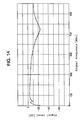
- Figs. 8 to 15 are graphs indicating examples of the pass characteristics of the RF modulators according to the present invention and the conventional techniques.
- the abscissa indicates a signal frequency, and is calibrated in 100 MHz increments from 2 to 1002 MHz.
- the ordinate indicates a signal level, and is calibrated in 10 dB increments in Figs. 8, 10, 12, and 14, and in 2 dB increments in Figs. 9, 11, 13, and 15.
- the level of 0 dB corresponds to no signal loss.
- Figs. 8 and 9 are graphs indicating the pass characteristics of the RF modulator of Fig. 1 when the amplifiers 7 and 8 are inactivated, the first switch 20 is on, and the second and third switches 21 and 22 are off. Figs. 8 and 9 show that signal loss is less than 2 dB.
- Figs. 10 and 11 are graphs indicating the pass characteristics of the conventional RF modulator of Fig. 6 when the amplifiers 7 and 8 are activated. Figs. 10 and 11 show the amplification of about 2 dB.
- Figs. 12 and 13 are graphs indicating the pass characteristics of the conventional RF modulator of Fig. 6 when the amplifiers 7 and 8 are inactivated. Figs. 12 and 13 show signal loss of about 30 to 40 dB. In this situation, the television signal cannot be received by a television receiver connected to the antenna output terminal 2.
- Figs. 14 and 15 are graphs indicating the pass characteristics of the conventional RF modulator of Fig. 7 when the amplifiers 7 and 8 are inactivated.
- the switch 15 is connected in parallel with the amplifiers 7 and 8 between the antenna input terminal 1 and the antenna output terminal 2.
- Figs. 14 and 15 show that signal loss in the construction of Fig. 7 is about 20 dB at a certain frequency, which is smaller than the signal loss in the construction of Fig. 6 as illustrated in Figs. 12 and 13, and much greater than the signal loss in the construction of Fig. 1.
- the signal loss in the construction of Fig. 7 is caused by the amplifiers 7 and 8 and the mixer 10.
- the RF modulator according to the present invention has the following advantages (1) and (2):
Landscapes
- Engineering & Computer Science (AREA)
- Multimedia (AREA)
- Signal Processing (AREA)
- Input Circuits Of Receivers And Coupling Of Receivers And Audio Equipment (AREA)
- Amplifiers (AREA)
- Color Television Systems (AREA)
Abstract
Description
- The present invention relates to a radio frequency (RF) modulator. The RF modulator according to the present invention may be used, for example, in video tape recorders, satellite broadcasting receivers, and the like.
- Conventionally, the construction of Fig. 6 is known as an RF modulator for use in the PAL (Phase Alternation by Line) color television system or the SECAM (séquential couleur á mémoire) system.
- In the construction of Fig. 6, the
antenna input terminal 1 is an input terminal, which is to be connected to an antenna, for receiving a television signal. Thetuner output terminal 3 is to be connected with a tuner unit, for supplying a received television signal to the tuner unit. The tuner unit is installed in a video tape recorder. Theantenna output terminal 2 is to be connected with an antenna terminal of an external television receiver, for outputting an amplified television signal, or a modulated signal. The amplified television signal is generated by amplifying by theamplifier 7 the television signal received through theantenna output terminal 2. The modulated signal is generated by themodulator 4 based on the video and audio signals respectively received through thevideo input terminal 5 and theaudio input terminal 6. The modulated signal has a predetermined channel frequency. - The
video input terminal 5 is to be connected with a video output terminal of the video tape recorder, for inputting the video signal, and theaudio input terminal 6 is to be connected with an audio output terminal of the video tape recorder, for inputting the audio signal. - The television signal received through the
antenna input terminal 1 is amplified by theamplifier 7, and is then distributed by thedistributor 9 to thetuner output terminal 3 and theantenna output terminal 2. The signal distributed to theantenna output terminal 2 is amplified by theamplifier 8, and input into themixer 10. Theamplifier 8 may be dispensed with. - The video signal and the audio signal which are input from the
video input terminal 5 and theaudio input terminal 6 are converted by themodulator 4 to a high-frequency modulated signal, and input into themixer 10. Themixer 10 is connected with theantenna output terminal 2 to output the modulated signal or the amplified television signal. - In the above RF modulator, even when the video tape recorder is not activated, i.e., even in a stand-by time, the path from the
antenna input terminal 1 to theantenna output terminal 2 must be kept active for the television signal, so that the television signal can be displayed on the external television receiver. That is, theamplifiers - In order to solve the above problem, Japanese Unexamined Utility Model Application No. 2-111946 discloses a technique as illustrated in Fig. 7. In the construction of Fig. 7, a
switch 15 is connected in parallel with theamplifiers antenna input terminal 1 and theantenna output terminal 2. Theswitch 15 is controlled to be off when theamplifiers amplifiers antenna input terminal 1 to theantenna output terminal 2 even when an electric power is not supplied to the construction of Fig. 7. - However, in the above RF modulator of Fig. 7, significant signal loss occurs when the
amplifiers switch 15 is on, since theantenna input terminal 1 and theamplifiers mixer 10 and theantenna output terminal 2 are also connected. - An object of the present invention is to provide a radio frequency (RF) modulator in which power consumption and signal loss during the stand-by time of the video tape recorder are reduced.
- According to the present invention, there is provided a radio frequency modulator containing a modulator which converts an input video signal and an input audio signal into a modulated signal having a predetermined channel frequency; an amplifier amplifying an input signal from an antenna input terminal; a mixer which mixes the modulated signal with the input signal amplified by the amplifier to output a mixed signal from an antenna output terminal; a first switch connected in parallel with the amplifier between the antenna input terminal and the antenna output terminal; a second switch connected between the antenna input terminal and the amplifier; and a third switch connected between the mixer and the antenna output terminal.
- In the above radio frequency modulator according to the present invention, the second switch may be controlled to be on when the amplifier is activated, and the second switch may be controlled to be off when the amplifier is inactivated. Thus, it is possible to prevent signal loss through the position of the second switch when the amplifier is inactivated.
- In the above radio frequency modulator according to the present invention, the third switch may be controlled to be on when the modulator or the amplifier is activated, and the third switch may be controlled to be off when both of the modulator and the amplifier are inactivated. Thus, it is possible to prevent signal loss through the position of the third switch when both of the modulator and the amplifier are inactivated.
- In the above radio frequency modulator according to the present invention, the first switch may be controlled to be off when the third switch is on, and the first switch may be controlled to be on when the third switch is off. Thus, it is possible to prevent signal loss through the position of the first switch when the third switch is on.
- In the above radio frequency modulator according to the present invention, the first switch may contain a switch circuit using a plurality of field effect transistors, and a transistor which is connected between at least two field effect transistors among the plurality of field effect transistors. The transistor grounds a signal leaked from the modulator when the at least two field effect transistors are in an unconductive state. Thus, signal loss can be further suppressed.
- In the drawings:
- Fig. 1 is a diagram illustrating the entire construction of the first embodiment of the present invention;
- Fig. 2 is a diagram illustrating the entire construction of the second embodiment of the present invention;
- Fig. 3 is a diagram illustrating the construction of the switch circuit in the third embodiment of the present invention;
- Fig. 4 is a diagram illustrating the construction of the switch circuit in the fourth embodiment of the present invention;
- Fig. 5 is a diagram illustrating the construction of the switch circuit in the fifth embodiment of the present invention;
- Fig. 6 is a diagram illustrating a conventional RF modulator;
- Fig. 7 is a diagram illustrating another conventional RF modulator;
- Fig. 8 is a graph indicating the pass characteristics of the RF modulator of Fig. 1 according to the present invention;
- Fig. 9 is a graph indicating the pass characteristics of the RF modulator of Fig. 1 according to the present invention;
- Fig. 10 is a graph indicating the pass characteristics of the conventional RF modulator of Fig. 6 when the amplifiers are activated;
- Fig. 11 is a graph indicating the pass characteristics of the conventional RF modulator of Fig. 6 when the amplifiers are activated;
- Fig. 12 is a graph indicating the pass characteristics of the conventional RF modulator of Fig. 6 when the amplifiers are inactivated;
- Fig. 13 is a graph indicating the pass characteristics of the conventional RF modulator of Fig. 6 when the amplifiers are inactivated;
- Fig. 14 is a graph indicating the pass characteristics of the conventional RF modulator of Fig. 7 when the amplifiers are inactivated; and
- Fig. 15 is a graph indicating the pass characteristics of the conventional RF modulator of Fig. 7 when the amplifiers are inactivated.
-
- The various embodiments of the present invention are explained below with reference to drawings. In the drawings referred to below, elements having the same reference numbers as Figs. 6 and 7 respectively function the same as the corresponding elements in Figs. 6 and 7, and therefore the explanations on such elements are not repeated below.
- Fig. 1 is a diagram illustrating the entire construction of the first embodiment of the present invention. In the construction of Fig. 1, the
first switch 20 is connected in parallel with theamplifiers antenna input terminal 1 and theantenna output terminal 2, thesecond switch 21 is connected between theantenna input terminal 1 and theamplifier 7, and thethird switch 22 is connected between themixer 10 and theantenna output terminal 2. - When the
amplifiers first switch 20 is turned off, and the second andthird switches antenna input terminal 1 is output through theamplifiers antenna output terminal 2. When theamplifiers first switch 20 is turned on, and the second andthird switches antenna input terminal 1 is output through thefirst switch 20 from theantenna output terminal 2. In this case, the received signal can reach theantenna output terminal 2 without influence of theamplifiers mixer 10. - The above first, second and
third switches amplifiers - Fig. 3 shows a construction of a switch circuit which is used as each of the second and
third switches power supply terminal 36, a current flows through theresistor 32, theswitching diode 31, and theresistor 33. The internal resistance of the switchingdiode 31 decreases when a current flows therethrough. Therefore, when a certain voltage is applied to thepower supply terminal 36, a signal can pass through the switchingdiode 31, i.e., the switch of Fig. 3 is turned on. When a certain voltage is not applied to thepower supply terminal 36, no current flows through the switchingdiode 31, the internal resistance of the switchingdiode 31 increases, and therefore the switch of Fig. 3 is turned off. The amount of the current flowing through the switchingdiode 31 is controlled by theresistors capacitors antenna input terminal 1 or theantenna output terminal 2. - Fig. 4 shows the construction of an FET switch circuit which is used as the
first switch 20 in the fourth embodiment of the present invention. In the construction of Fig. 4, the FET (field effect transistor) 41 is an n-channel FET performing a switching action. When no voltage is applied to thepower supply terminal 47, the gate and the source of theFET 41 are at the same potential, and therefore a current flows between the source and the drain of theFET 41, i.e., theFET 41 is turned on. When a certain voltage is applied to thepower supply terminal 47, the potential of the gate becomes lower than the potential of the source of theFET 41 due to voltage drop in theresistor 43, and therefore a current does not flow between the source and the drain of theFET 41, i.e., theFET 41 is turned off. Thecapacitors - In the construction of Fig. 1, when the
modulator 4 is activated, thethird switch 22 is on, and thefirst switch 20 is off. If the first switch is an electronic switch, and the electronic switch does not achieve sufficient insulation, a portion of the output of themodulator 4 may leak through thefirst switch 20 to theantenna input terminal 1. In order to prevent such leakage, it is possible to lift the insulation level by providing more than one first switch, or connecting one or more transistors in the channel. The construction of Fig. 5 is one example of such provision. - Fig. 5 is a diagram illustrating the construction of the switch circuit in the fifth embodiment of the present invention. The
FETs FET 41 in Fig. 4, theresistors resistor 42 in Fig. 4, theresistors resistor 43 in Fig. 4, theresistors resistor 44 in Fig. 4, thecapacitors capacitors power supply terminals power supply terminal 47 in Fig. 4. In addition, in the construction of Fig. 5, anNPN transistor 61 is connected to a path between theFETs resistors transistor 61. Theresistor 62 is a protection resistor, and one end of theresistors 62 is anotherpower supply terminal 64. Theresistor 63 is provided so that the potentials of the base and the emitter of thetransistor 61 become the same level when no voltage is applied to thepower supply terminal 64. - Thus, when no voltage is applied to the
power supply terminal 64, the potentials of the base and the emitter of thetransistor 61 are the same level due to the provision of theresistor 63, the collector and the emitter become open, and therefore thetransistor 61 does not influence the signal path between theFETs power supply terminal 64, the potential of the base of thetransistor 61 becomes higher than the potential of the emitter, and therefore a current flows from the collector to the emitter of thetransistor 61, i.e., thetransistor 61 is turned on. Therefore, it is possible to ground the signal leaked from themodulator 4 when theFETs - Figs. 8 to 15 are graphs indicating examples of the pass characteristics of the RF modulators according to the present invention and the conventional techniques. In each of the graphs, the abscissa indicates a signal frequency, and is calibrated in 100 MHz increments from 2 to 1002 MHz. The ordinate indicates a signal level, and is calibrated in 10 dB increments in Figs. 8, 10, 12, and 14, and in 2 dB increments in Figs. 9, 11, 13, and 15. The level of 0 dB corresponds to no signal loss.
- Figs. 8 and 9 are graphs indicating the pass characteristics of the RF modulator of Fig. 1 when the
amplifiers first switch 20 is on, and the second andthird switches - Figs. 10 and 11 are graphs indicating the pass characteristics of the conventional RF modulator of Fig. 6 when the
amplifiers - Figs. 12 and 13 are graphs indicating the pass characteristics of the conventional RF modulator of Fig. 6 when the
amplifiers antenna output terminal 2. - Figs. 14 and 15 are graphs indicating the pass characteristics of the conventional RF modulator of Fig. 7 when the
amplifiers switch 15 is connected in parallel with theamplifiers antenna input terminal 1 and theantenna output terminal 2. Figs. 14 and 15 show that signal loss in the construction of Fig. 7 is about 20 dB at a certain frequency, which is smaller than the signal loss in the construction of Fig. 6 as illustrated in Figs. 12 and 13, and much greater than the signal loss in the construction of Fig. 1. As explained before, it is considered that the signal loss in the construction of Fig. 7 is caused by theamplifiers mixer 10. - Thus, according to the present invention, the power consumption and the signal loss in the stand-by time can be suppressed. In addition, the RF modulator according to the present invention has the following advantages (1) and (2):
- (1) When unnecessary signals other than a desired
signal are input through the
antenna input terminal 1, and is then amplified by theamplifiers antenna output terminal 2. However, when a user wishes to watch a first television program in a first television channel, and concurrently record a second television program in a second television channel in the construction of Fig. 1, the television signal of the first channel can bypass theamplifiers tuner output terminal 3 can receive a television signal of the second channel after amplified by theamplifier 7, when theamplifiers second switches third switch 22 is turned off. Thus, the television receiver can receive the desired television signal of the first channel from theantenna input terminal 1 without the above interference. - (2) When the user wishes to watch on the television
receiver a playback video picture from the video tape
recorder through the
modulator 4 in the construction of Fig. 1, theamplifiers second switches third switch 22 should be turned on. In this configuration, the playback signal from the video tape recorder is converted by themodulator 4 into a modulated signal, and is supplied to the television receiver through theantenna output terminal 2. In this case, a current through theamplifiers amplifiers antenna input terminal 1 can be suppressed. -
- All of the contents of the Japanese patent application, No. 11-29129 are incorporated into this specification by reference.
- All publications, patents and patent applications cited herein are incorporated herein by reference in their entirety.
Claims (5)
- A radio frequency modulator comprising:a modulator which converts an input video signal and an input audio signal into a modulated signal having a predetermined channel frequency;an amplifier amplifying an input signal from an antenna input terminal;a mixer which mixes said modulated signal with said input signal amplified by the amplifier to output a mixed signal from an antenna output terminal;a first switch connected in parallel with said amplifier between said antenna input terminal and said antenna output terminal;a second switch connected between said antenna input terminal and said amplifier; anda third switch connected between said mixer and said antenna output terminal.
- A radio frequency modulator according to claim 1, wherein said second switch is controlled to be on when said amplifier is activated, and said second switch is controlled to be off when said amplifier is inactivated.
- A radio frequency modulator according to claim 1, wherein said third switch is controlled to be on when said modulator or said amplifier is activated, and said third switch is controlled to be off when said modulator and said amplifier are inactivated.
- A radio frequency modulator according to claim 1, wherein said first switch is controlled to be off when said third switch is on, and said first switch is controlled to be on when said third switch is off.
- A radio frequency modulator according to claim 1, wherein said first switch contains a switch circuit using a plurality of field effect transistors, and a transistor which is connected between at least two field effect transistors among the plurality of field effect transistors, where said transistor grounds a signal leaked from said modulator when said at least two field effect transistors are in an unconductive state.
Applications Claiming Priority (2)
| Application Number | Priority Date | Filing Date | Title |
|---|---|---|---|
| JP2912999 | 1999-02-05 | ||
| JP02912999A JP3526771B2 (en) | 1999-02-05 | 1999-02-05 | RF modulator device |
Publications (2)
| Publication Number | Publication Date |
|---|---|
| EP1026821A2 true EP1026821A2 (en) | 2000-08-09 |
| EP1026821A3 EP1026821A3 (en) | 2002-06-05 |
Family
ID=12267699
Family Applications (1)
| Application Number | Title | Priority Date | Filing Date |
|---|---|---|---|
| EP00300751A Ceased EP1026821A3 (en) | 1999-02-05 | 2000-01-31 | Radio frequency modulator having isolation switches and signal path bypassing amplifier and modulator |
Country Status (5)
| Country | Link |
|---|---|
| EP (1) | EP1026821A3 (en) |
| JP (1) | JP3526771B2 (en) |
| CN (1) | CN1111331C (en) |
| MY (1) | MY123994A (en) |
| TW (1) | TW459446B (en) |
Cited By (2)
| Publication number | Priority date | Publication date | Assignee | Title |
|---|---|---|---|---|
| EP1276322A1 (en) * | 2001-07-10 | 2003-01-15 | Matsushita Electric Industrial Co., Ltd | Satellite receiver and operation method |
| US7919307B2 (en) | 2005-05-09 | 2011-04-05 | Alpha Plan Gmbh | Supply system for cell culture module |
Families Citing this family (5)
| Publication number | Priority date | Publication date | Assignee | Title |
|---|---|---|---|---|
| CN101820542A (en) * | 2010-03-04 | 2010-09-01 | 上海大学 | Video transmission method for effectively controlling unequal power consumption |
| JP6219598B2 (en) * | 2013-05-23 | 2017-10-25 | 新日本無線株式会社 | High frequency power distributor |
| CN107302382A (en) * | 2017-06-22 | 2017-10-27 | 上海傲蓝信息科技有限公司 | A kind of data communication system based on rf-signal modulation signal |
| CN108322624A (en) * | 2017-12-29 | 2018-07-24 | 河南北瑞电子科技有限公司 | A kind of radio-frequency modulator |
| CN116094540B (en) * | 2022-12-12 | 2025-08-19 | 维沃移动通信有限公司 | Radio frequency path and electronic equipment |
Citations (1)
| Publication number | Priority date | Publication date | Assignee | Title |
|---|---|---|---|---|
| US4400735A (en) * | 1981-07-10 | 1983-08-23 | Zenith Radio Corporation | Multi-component video system controller |
Family Cites Families (5)
| Publication number | Priority date | Publication date | Assignee | Title |
|---|---|---|---|---|
| US4894720A (en) * | 1987-07-31 | 1990-01-16 | Sanyo Electric Co., Ltd. | Circuit for selectively outputting high frequency signals |
| KR960008728B1 (en) * | 1992-09-30 | 1996-06-29 | Samsung Electro Mech | High frequency switching circuit of vcr |
| DE59508022D1 (en) * | 1994-04-21 | 2000-04-27 | Koninkl Philips Electronics Nv | Circuit arrangement for feeding an antenna signal |
| JP3481388B2 (en) * | 1995-08-30 | 2003-12-22 | アルプス電気株式会社 | Antenna booster mixer circuit |
| GB2313238A (en) * | 1996-05-14 | 1997-11-19 | Alps Electric Co Ltd | Antenna booster mixer circuit |
-
1999
- 1999-02-05 JP JP02912999A patent/JP3526771B2/en not_active Expired - Fee Related
-
2000
- 2000-01-31 EP EP00300751A patent/EP1026821A3/en not_active Ceased
- 2000-01-31 TW TW089101629A patent/TW459446B/en active
- 2000-02-02 MY MYPI20000354 patent/MY123994A/en unknown
- 2000-02-04 CN CN00106713A patent/CN1111331C/en not_active Expired - Fee Related
Patent Citations (1)
| Publication number | Priority date | Publication date | Assignee | Title |
|---|---|---|---|---|
| US4400735A (en) * | 1981-07-10 | 1983-08-23 | Zenith Radio Corporation | Multi-component video system controller |
Cited By (2)
| Publication number | Priority date | Publication date | Assignee | Title |
|---|---|---|---|---|
| EP1276322A1 (en) * | 2001-07-10 | 2003-01-15 | Matsushita Electric Industrial Co., Ltd | Satellite receiver and operation method |
| US7919307B2 (en) | 2005-05-09 | 2011-04-05 | Alpha Plan Gmbh | Supply system for cell culture module |
Also Published As
| Publication number | Publication date |
|---|---|
| CN1111331C (en) | 2003-06-11 |
| TW459446B (en) | 2001-10-11 |
| EP1026821A3 (en) | 2002-06-05 |
| JP3526771B2 (en) | 2004-05-17 |
| MY123994A (en) | 2006-06-30 |
| JP2000228749A (en) | 2000-08-15 |
| CN1266310A (en) | 2000-09-13 |
Similar Documents
| Publication | Publication Date | Title |
|---|---|---|
| JP3526771B2 (en) | RF modulator device | |
| US5374895A (en) | NMR/MRI pulse amplifier | |
| US5003620A (en) | Tuner circuit and receiving band change-over circuit with a push-pull amplifier | |
| KR100211755B1 (en) | Antenna booster mixer circuit | |
| US4710737A (en) | Band switching circuit tuner | |
| JP2844609B2 (en) | AGC circuit | |
| GB2157906A (en) | High-frequency switching circuit | |
| EP0990345A2 (en) | Video recorder/reproducer apparatus | |
| US4065681A (en) | Voltage storage circuit useful in television receiver control applications | |
| JP3565739B2 (en) | Television tuner | |
| US5412482A (en) | Signal line changeover circuit with emitter followers | |
| JPH0339958Y2 (en) | ||
| JPS60220623A (en) | High frequency switching circuit | |
| JPH0735456Y2 (en) | RF switch circuit | |
| GB2313238A (en) | Antenna booster mixer circuit | |
| JPS6325799Y2 (en) | ||
| US6891574B1 (en) | High speed video mixer circuit | |
| JPS6031334Y2 (en) | High frequency signal switching device | |
| KR0116895Y1 (en) | RF input switching circuit of BS tuner | |
| JPH06125503A (en) | Signal distributor | |
| KR940001617Y1 (en) | Audio-only recording control circuit of hi-fi video tape recorder | |
| KR960005925B1 (en) | Bs receiver using broadcasting system control apparatus | |
| JPH0514618Y2 (en) | ||
| US6266099B1 (en) | Video on-screen display with reduced feedthrough and crosstalk | |
| KR950002559Y1 (en) | Booster output signal switching circuit of high frequency modulator |
Legal Events
| Date | Code | Title | Description |
|---|---|---|---|
| PUAI | Public reference made under article 153(3) epc to a published international application that has entered the european phase |
Free format text: ORIGINAL CODE: 0009012 |
|
| AK | Designated contracting states |
Kind code of ref document: A2 Designated state(s): AT BE CH CY DE DK ES FI FR GB GR IE IT LI LU MC NL PT SE |
|
| AX | Request for extension of the european patent |
Free format text: AL;LT;LV;MK;RO;SI |
|
| PUAL | Search report despatched |
Free format text: ORIGINAL CODE: 0009013 |
|
| AK | Designated contracting states |
Kind code of ref document: A3 Designated state(s): AT BE CH CY DE DK ES FI FR GB GR IE IT LI LU MC NL PT SE |
|
| AX | Request for extension of the european patent |
Free format text: AL;LT;LV;MK;RO;SI |
|
| RIC1 | Information provided on ipc code assigned before grant |
Free format text: 7H 03C 5/00 A, 7H 04N 5/44 B, 7H 04N 5/775 B |
|
| 17P | Request for examination filed |
Effective date: 20021105 |
|
| AKX | Designation fees paid |
Designated state(s): DE FR GB |
|
| 17Q | First examination report despatched |
Effective date: 20060802 |
|
| STAA | Information on the status of an ep patent application or granted ep patent |
Free format text: STATUS: THE APPLICATION HAS BEEN REFUSED |
|
| 18R | Application refused |
Effective date: 20091122 |