EP1026489A1 - Contact temperature probe with thermal isolation - Google Patents
Contact temperature probe with thermal isolation Download PDFInfo
- Publication number
- EP1026489A1 EP1026489A1 EP00300701A EP00300701A EP1026489A1 EP 1026489 A1 EP1026489 A1 EP 1026489A1 EP 00300701 A EP00300701 A EP 00300701A EP 00300701 A EP00300701 A EP 00300701A EP 1026489 A1 EP1026489 A1 EP 1026489A1
- Authority
- EP
- European Patent Office
- Prior art keywords
- probe
- probe head
- lead wires
- temperature
- temperature probe
- Prior art date
- Legal status (The legal status is an assumption and is not a legal conclusion. Google has not performed a legal analysis and makes no representation as to the accuracy of the status listed.)
- Granted
Links
- 239000000523 sample Substances 0.000 title claims abstract description 46
- 238000002955 isolation Methods 0.000 title description 3
- 238000000034 method Methods 0.000 claims abstract description 7
- 239000011324 bead Substances 0.000 claims description 10
- 239000004065 semiconductor Substances 0.000 claims description 9
- 239000000919 ceramic Substances 0.000 claims description 6
- 235000012431 wafers Nutrition 0.000 description 13
- 239000010453 quartz Substances 0.000 description 7
- VYPSYNLAJGMNEJ-UHFFFAOYSA-N silicon dioxide Inorganic materials O=[Si]=O VYPSYNLAJGMNEJ-UHFFFAOYSA-N 0.000 description 7
- 238000005259 measurement Methods 0.000 description 6
- 238000009529 body temperature measurement Methods 0.000 description 2
- 238000010438 heat treatment Methods 0.000 description 2
- 230000005855 radiation Effects 0.000 description 2
- 230000000717 retained effect Effects 0.000 description 2
- 239000010935 stainless steel Substances 0.000 description 2
- 229910001220 stainless steel Inorganic materials 0.000 description 2
- 229910000809 Alumel Inorganic materials 0.000 description 1
- YCKRFDGAMUMZLT-UHFFFAOYSA-N Fluorine atom Chemical compound [F] YCKRFDGAMUMZLT-UHFFFAOYSA-N 0.000 description 1
- 229910000990 Ni alloy Inorganic materials 0.000 description 1
- 229910001179 chromel Inorganic materials 0.000 description 1
- 238000002788 crimping Methods 0.000 description 1
- 229910052731 fluorine Inorganic materials 0.000 description 1
- 239000011737 fluorine Substances 0.000 description 1
- 239000011521 glass Substances 0.000 description 1
- 238000009413 insulation Methods 0.000 description 1
- 238000003466 welding Methods 0.000 description 1
Images
Classifications
-
- G—PHYSICS
- G01—MEASURING; TESTING
- G01K—MEASURING TEMPERATURE; MEASURING QUANTITY OF HEAT; THERMALLY-SENSITIVE ELEMENTS NOT OTHERWISE PROVIDED FOR
- G01K7/00—Measuring temperature based on the use of electric or magnetic elements directly sensitive to heat ; Power supply therefor, e.g. using thermoelectric elements
-
- G—PHYSICS
- G01—MEASURING; TESTING
- G01K—MEASURING TEMPERATURE; MEASURING QUANTITY OF HEAT; THERMALLY-SENSITIVE ELEMENTS NOT OTHERWISE PROVIDED FOR
- G01K1/00—Details of thermometers not specially adapted for particular types of thermometer
- G01K1/16—Special arrangements for conducting heat from the object to the sensitive element
-
- G—PHYSICS
- G01—MEASURING; TESTING
- G01K—MEASURING TEMPERATURE; MEASURING QUANTITY OF HEAT; THERMALLY-SENSITIVE ELEMENTS NOT OTHERWISE PROVIDED FOR
- G01K1/00—Details of thermometers not specially adapted for particular types of thermometer
- G01K1/14—Supports; Fastening devices; Arrangements for mounting thermometers in particular locations
- G01K1/143—Supports; Fastening devices; Arrangements for mounting thermometers in particular locations for measuring surface temperatures
Definitions
- the present invention is directed to an improved contact temperature probe for measuring the temperature of a semiconductor wafer being processed, and particularly to a temperature probe which provides more accurate temperature readings.
- a contact temperature probe having a probe head which pivots under the weight of a semiconductor wafer, so as to maintain close contact therewith.
- Fig. 12 of such patent an embodiment is disclosed wherein the probe head is set on and pivots on the lip of a quartz shield through which the temperature sensor lead wires are run to protect the wires from the process environment.
- a contact temperature probe having a probe head including a flat contact surface for contacting the semiconductor wafer and a body which houses a temperature sensor having lead wires which exit the body and run through a shield for shielding the wires from the process environment, wherein the probe head is supported only by the temperature sensor lead wires and the shield does not touch the probe head.
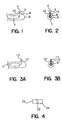
- a side view of an embodiment of the invention is depicted, and is seen to be comprised of probe head 2 having flat contact surface 4 for contacting a semiconductor wafer, and quartz shield 6 for shielding the temperature sensor wires from the process environment.
- the wafer may be supported on three supports, for example, two glass pegs and the device shown in Fig. 1.
- Such an arrangement is shown in Fig. 6 of the above-mentioned U.S. Patent No. 5,791,782 the entire contents of which are herein incorporated by reference.
- the probe head sets on lip 8 of quartz shield 6 herein and pivots thereon under the weight of the semiconductor wafer.
- the accuracy of the temperature measurement provided by this device is not good enough for some applications.
- the probe head is supported only by the temperature sensor wires 10 and 12, and is thermally isolated from the quartz shield.
- the thermal isolation reduces the effective thermal mass, and causes the temperature sensor to more closely follow the temperature of the wafer.
- the temperature sensor is a thermocouple.
- a thermocouple As known to those skilled in the art, such a device is formed by creating a bead from two metallic wires of predetermined properties. Referring to Fig. 4, a probe head 20 is shown having a centered, axial, blind hole 22 extending from the lower surface 24. The thermocouple bead is inserted in this hole. The hole is then collapsed by a crimping operation around the thermocouple as described in detail in the above-mentioned U.S. Patent No. 5,791,782. This creates good electrical contact between the two wires at the bead and good thermal contact between the probe head and the thermocouple.
- sensor wires 10 and 12 form two legs of a triangle having an apex at the head.
- the wires are of suitable stiffness to support the probe head by themselves while allowing pivoting of the head around the bead under the weight of the wafer.
- isolation of the probe head from the quartz shield is achieved while the pivoting action of the probe head on its support is retained, so as to ensure intimate contact between the probe head and the wafer and correspondingly low contact resistance.
- a device which is mechanically more robust than that of the prior art is provided.
- the quartz shield 6 encloses a stainless steel tube 7 which protects the thermocouple wires from electrical signals.
- a ceramic tube 9 having two longitudinally extending openings through which the wires are run. The ceramic tube provides heat insulation for the thermocouple wires.
- the processing of semiconductor wafers sometimes includes exposing the wafer to ultraviolet or other radiation, which may be emitted by lamps.
- ultraviolet or other radiation which may be emitted by lamps.
- the ceramic sheath is extended to cover the entire portion of the wire which runs in the longitudinal direction of the quartz shield, thus minimizing lamp heating of the wires.
- Fig. 3 shows a further embodiment of the invention which is a similar structure to the embodiment of Figs. 1 and 2, but where the two wires 10' and 12' are welded together to form bead 13.
- the welding creates better contact at the junction, then with an unwelded bead (typically formed by merely intertwining the wires), and results in less electrical noise.
- the probe head is made substantially smaller than in prior art, in that it is arranged to have a diameter of less than .1". While providing a suitable contact surface, this results in less thermal mass, with a consequently faster response time as well as less variation in response due to heating from external heat sources such as lamps which may be used in the processing. The result is more consistently repeatable measurements, which is illustrated in the graphs of Figs. 5 and 6.
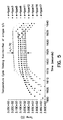
- Figs. 5 is a graph depicting temperature response for different runs using different individual prior art probe heads of the type disclosed in U.S. Patent No. 5,791,782. As can be seen, the consistency of the repeated measurements is within ⁇ 7°C.
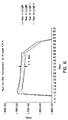
- Fig. 6 is a graph which depicts temperature response for different runs using different individual probe heads made according the present invention. As can be seen, in the case of Fig. 6, the consistency of the repeated measurements is within ⁇ 2°C, which is a substantial improvement.
- the diameter of the probe head was .073
- the thermocouple wire was made of a nickel alloy such as chromel alumel, to be fluorine resistant.
- the thermocouple was a type K device.
Landscapes
- Physics & Mathematics (AREA)
- General Physics & Mathematics (AREA)
- Testing Or Measuring Of Semiconductors Or The Like (AREA)
- Measuring Temperature Or Quantity Of Heat (AREA)
Abstract
Description
- The present invention is directed to an improved contact temperature probe for measuring the temperature of a semiconductor wafer being processed, and particularly to a temperature probe which provides more accurate temperature readings.
- In U.S. Patent No, 5,791,782, a contact temperature probe is disclosed having a probe head which pivots under the weight of a semiconductor wafer, so as to maintain close contact therewith. In Fig. 12 of such patent, an embodiment is disclosed wherein the probe head is set on and pivots on the lip of a quartz shield through which the temperature sensor lead wires are run to protect the wires from the process environment.
- While the concept of a pivoting probe head results in reduced contact resistance between the wafer and the probe head, it has been found that the temperature measurements which are afforded by the prior art probe are not as accurate as is desired.
- It is thus one object of the invention to provide a contact temperature probe which provides more accurate measurements.
- In accordance with the invention, the above as well as other objects are obtained by providing a contact temperature probe having a probe head including a flat contact surface for contacting the semiconductor wafer and a body which houses a temperature sensor having lead wires which exit the body and run through a shield for shielding the wires from the process environment, wherein the probe head is supported only by the temperature sensor lead wires and the shield does not touch the probe head.
- The invention will be better appreciated by referring to the accompanying drawings wherein,
- Fig. 1 is a side view of an embodiment of the invention.
- Fig. 2 is an approximately vertical sectional view taken through V lead wires of Fig. 1.
- Fig. 3 shows a further embodiment of the invention.
- Fig. 4 shows a probe head.
- Fig. 5 is a graph showing temperature sensor consistency of measurement for a prior art device.
- Fig. 6 is a graph showing temperature sensor consistency of measurement for an embodiment of the present invention.
-
- Referring to Fig. 1, a side view of an embodiment of the invention is depicted, and is seen to be comprised of
probe head 2 havingflat contact surface 4 for contacting a semiconductor wafer, andquartz shield 6 for shielding the temperature sensor wires from the process environment. In the process chamber, the wafer may be supported on three supports, for example, two glass pegs and the device shown in Fig. 1. Such an arrangement is shown in Fig. 6 of the above-mentioned U.S. Patent No. 5,791,782 the entire contents of which are herein incorporated by reference. - In the arrangement of the prior patent, the probe head sets on
lip 8 ofquartz shield 6 herein and pivots thereon under the weight of the semiconductor wafer. However, as mentioned above, the accuracy of the temperature measurement provided by this device is not good enough for some applications. - In accordance with the present invention, the probe head is supported only by the
temperature sensor wires - At the same time, the pivoting motion of the probe head under the weight of the wafer is retained, as will be explained below.
- In the preferred embodiment, the temperature sensor is a thermocouple. As known to those skilled in the art, such a device is formed by creating a bead from two metallic wires of predetermined properties. Referring to Fig. 4, a
probe head 20 is shown having a centered, axial,blind hole 22 extending from thelower surface 24. The thermocouple bead is inserted in this hole. The hole is then collapsed by a crimping operation around the thermocouple as described in detail in the above-mentioned U.S. Patent No. 5,791,782. This creates good electrical contact between the two wires at the bead and good thermal contact between the probe head and the thermocouple. - Referring again to Figs. 1 and 2, it is seen that
sensor wires - The
quartz shield 6 encloses astainless steel tube 7 which protects the thermocouple wires from electrical signals. Within thestainless steel tube 7 is aceramic tube 9 having two longitudinally extending openings through which the wires are run. The ceramic tube provides heat insulation for the thermocouple wires. - The processing of semiconductor wafers sometimes includes exposing the wafer to ultraviolet or other radiation, which may be emitted by lamps. In the prior art, it was found that such radiation heated the thermocouple wires and resulted in inaccurate temperature readings. In accordance with an improvement of the present invention, the ceramic sheath is extended to cover the entire portion of the wire which runs in the longitudinal direction of the quartz shield, thus minimizing lamp heating of the wires.
- Fig. 3 shows a further embodiment of the invention which is a similar structure to the embodiment of Figs. 1 and 2, but where the two wires 10' and 12' are welded together to form
bead 13. The welding creates better contact at the junction, then with an unwelded bead (typically formed by merely intertwining the wires), and results in less electrical noise. - In accordance with a further feature of the invention, the probe head is made substantially smaller than in prior art, in that it is arranged to have a diameter of less than .1". While providing a suitable contact surface, this results in less thermal mass, with a consequently faster response time as well as less variation in response due to heating from external heat sources such as lamps which may be used in the processing. The result is more consistently repeatable measurements, which is illustrated in the graphs of Figs. 5 and 6.
- Figs. 5 is a graph depicting temperature response for different runs using different individual prior art probe heads of the type disclosed in U.S. Patent No. 5,791,782. As can be seen, the consistency of the repeated measurements is within ±7°C.
- Fig. 6 is a graph which depicts temperature response for different runs using different individual probe heads made according the present invention. As can be seen, in the case of Fig. 6, the consistency of the repeated measurements is within ±2°C, which is a substantial improvement.
- In the actual embodiment of the invention which produced the results shown in Fig. 6, the diameter of the probe head was .073", and the thermocouple wire was made of a nickel alloy such as chromel alumel, to be fluorine resistant. The thermocouple was a type K device.
- Thus, an improved contact temperature probe had been disclosed. Variation will occur to those skilled in that which do not depart from the spirit of the invention and it should be understood that the subject matter to be covered is defined by the claims appended hereto.
Claims (6)
- A contact temperature probe for measuring the temperature of a semiconductor wafer in a process environment, comprising:a contact temperature probe head (2, 20) including a flat contact surface (4) for contacting the semiconductor wafer and a body which houses a temperature sensor (13) having lead wires (10, 12, 10', 12') which exit the body and run through a shield (6) for shielding the wires from the process environment,
wherein the probe head is supported only by the temperature sensor lead wires, and the shield does not touch the probe head. - The temperature probe of claim 1 wherein the temperature sensor is a thermocouple bead (13) which is formed by electrically contacting the lead wires with each other, and wherein the lead wires form two legs of a triangle having an apex at the bead, and are stiff enough to support the probe head while allowing pivoting movement of the probe head around the bead under the weight of the semiconductor wafer.
- The temperature probe of claim 2 wherein the lead wires are welded together to form the bead (13).
- The temperature probe of claim 2 wherein the shield is longitudinally extending, and there is a longitudinally extending ceramic sheath (9) in the shield, and a portion of the lead wires extend in the longitudinal direction of the sheath and pass through the sheath.
- The temperature probe of claim 4 wherein the ceramic sheath encloses substantially the entire portion of the lead wires which extend in the longitudinal direction of the ceramic sheath.
- The temperature probe of claim 2, wherein the diameter of the probe head is less than .1".
Applications Claiming Priority (2)
| Application Number | Priority Date | Filing Date | Title |
|---|---|---|---|
| US11817599P | 1999-02-01 | 1999-02-01 | |
| US118175P | 1999-02-01 |
Publications (2)
| Publication Number | Publication Date |
|---|---|
| EP1026489A1 true EP1026489A1 (en) | 2000-08-09 |
| EP1026489B1 EP1026489B1 (en) | 2007-04-25 |
Family
ID=22376952
Family Applications (1)
| Application Number | Title | Priority Date | Filing Date |
|---|---|---|---|
| EP00300701A Expired - Lifetime EP1026489B1 (en) | 1999-02-01 | 2000-01-31 | Contact temperature probe with thermal isolation between probe head and heat shield of sensor wires |
Country Status (5)
| Country | Link |
|---|---|
| US (1) | US6332709B1 (en) |
| EP (1) | EP1026489B1 (en) |
| JP (1) | JP2000227363A (en) |
| KR (1) | KR20010006600A (en) |
| DE (1) | DE60034496T2 (en) |
Cited By (2)
| Publication number | Priority date | Publication date | Assignee | Title |
|---|---|---|---|---|
| KR20010006600A (en) * | 1999-02-01 | 2001-01-26 | 브라이언 알. 바흐맨 | Contact temperature probe with thermal isolation |
| DE102005016896B3 (en) * | 2005-04-12 | 2006-10-26 | Sitronic Gesellschaft für elektrotechnische Ausrüstung mbH. & Co. KG | Sensor arrangement for temperature measurement |
Families Citing this family (11)
| Publication number | Priority date | Publication date | Assignee | Title |
|---|---|---|---|---|
| US6796711B2 (en) | 2002-03-29 | 2004-09-28 | Axcelis Technologies, Inc. | Contact temperature probe and process |
| US7018096B2 (en) * | 2003-04-25 | 2006-03-28 | Universal Leaf Tobacco Company, Inc. | Packed product temperature measuring device |
| US7651269B2 (en) * | 2007-07-19 | 2010-01-26 | Lam Research Corporation | Temperature probes having a thermally isolated tip |
| JP5184334B2 (en) * | 2008-12-26 | 2013-04-17 | 山里産業株式会社 | Probe for temperature measurement |
| WO2010088237A1 (en) * | 2009-01-30 | 2010-08-05 | Embedded Designs Inc. | Method and apparatus for measuring part temperature through a conveyorized thermal processor |
| CN102944120B (en) * | 2012-11-19 | 2014-07-09 | 中山大学 | Integral multifunctional sintering furnace temperature inspection instrument carrier |
| DE202015103789U1 (en) * | 2015-07-17 | 2015-07-31 | Abb Technology Ag | Surface temperature sensor |
| US10753807B2 (en) | 2018-01-19 | 2020-08-25 | Te Wire & Cable Llc | Thermocouple termination/closure and method |
| US11415463B2 (en) * | 2019-06-04 | 2022-08-16 | Applied Materials, Inc. | Contactless workpiece temperature sensor |
| GB201910045D0 (en) * | 2019-07-12 | 2019-08-28 | Nicoventures Trading Ltd | Aerosol provision systems |
| EP3951339B1 (en) * | 2020-08-06 | 2022-10-05 | Qnami AG | Nanoscale thermometry |
Citations (2)
| Publication number | Priority date | Publication date | Assignee | Title |
|---|---|---|---|---|
| DE4244189A1 (en) * | 1992-12-24 | 1994-07-07 | Busch Dieter & Co Prueftech | Contact temperature sensor |
| US5791782A (en) * | 1995-09-21 | 1998-08-11 | Fusion Systems Corporation | Contact temperature probe with unrestrained orientation |
Family Cites Families (17)
| Publication number | Priority date | Publication date | Assignee | Title |
|---|---|---|---|---|
| DE2047539C3 (en) * | 1970-09-26 | 1973-09-20 | Gesellschaft Fuer Kernforschung Mbh, 7500 Karlsruhe | Thermocouple |
| JPH0323548Y2 (en) * | 1981-06-19 | 1991-05-22 | ||
| JPS6438619A (en) * | 1987-08-04 | 1989-02-08 | Anritsu Meter | Surface temperature sensor |
| US4871263A (en) * | 1988-05-16 | 1989-10-03 | Pyromation, Inc. | Protective tube for a temperature sensor |
| JPH03175625A (en) * | 1989-12-04 | 1991-07-30 | Nec Corp | Method and apparatus for heat treatment of semiconductor device |
| US5356486A (en) * | 1991-03-04 | 1994-10-18 | Applied Materials, Inc. | Combined wafer support and temperature monitoring device |
| JP2979264B2 (en) * | 1991-04-05 | 1999-11-15 | 安立計器株式会社 | Contact temperature sensor |
| KR930006305B1 (en) * | 1991-07-09 | 1993-07-12 | 한국과학기술연구원 | Wafer-temperature detecting apparatus |
| JPH05118928A (en) * | 1991-10-25 | 1993-05-14 | Tokyo Electron Ltd | Contact temperature measurement method |
| US5193912A (en) * | 1991-11-18 | 1993-03-16 | Saunders Roger I | Probe for sensing and measuring temperature |
| US5321719A (en) * | 1993-05-26 | 1994-06-14 | Ta Instruments, Inc. | Thermogravimetric apparatus |
| US5370459A (en) * | 1993-06-08 | 1994-12-06 | Claud S. Gordon Company | Surface temperature probe with uniform thermocouple junction |
| JP3760527B2 (en) * | 1996-11-06 | 2006-03-29 | 株式会社村田製作所 | Temperature measuring device |
| JP3709257B2 (en) * | 1997-05-14 | 2005-10-26 | 安立計器株式会社 | Contact thermometer |
| US6257758B1 (en) * | 1998-10-09 | 2001-07-10 | Claud S. Gordon Company | Surface temperature sensor |
| US6040518A (en) * | 1998-12-22 | 2000-03-21 | Eaton Corporation | Wafer temperature monitoring device utilizing flexible thermocouple |
| EP1026489B1 (en) * | 1999-02-01 | 2007-04-25 | Axcelis Technologies, Inc. | Contact temperature probe with thermal isolation between probe head and heat shield of sensor wires |
-
2000
- 2000-01-31 EP EP00300701A patent/EP1026489B1/en not_active Expired - Lifetime
- 2000-01-31 DE DE60034496T patent/DE60034496T2/en not_active Expired - Lifetime
- 2000-02-01 JP JP2000023861A patent/JP2000227363A/en active Pending
- 2000-02-01 KR KR1020000004848A patent/KR20010006600A/en not_active Ceased
- 2000-02-01 US US09/495,704 patent/US6332709B1/en not_active Expired - Lifetime
Patent Citations (2)
| Publication number | Priority date | Publication date | Assignee | Title |
|---|---|---|---|---|
| DE4244189A1 (en) * | 1992-12-24 | 1994-07-07 | Busch Dieter & Co Prueftech | Contact temperature sensor |
| US5791782A (en) * | 1995-09-21 | 1998-08-11 | Fusion Systems Corporation | Contact temperature probe with unrestrained orientation |
Cited By (3)
| Publication number | Priority date | Publication date | Assignee | Title |
|---|---|---|---|---|
| KR20010006600A (en) * | 1999-02-01 | 2001-01-26 | 브라이언 알. 바흐맨 | Contact temperature probe with thermal isolation |
| US6332709B1 (en) * | 1999-02-01 | 2001-12-25 | Axcelis Technologies, Inc. | Contact temperature probe with thermal isolation |
| DE102005016896B3 (en) * | 2005-04-12 | 2006-10-26 | Sitronic Gesellschaft für elektrotechnische Ausrüstung mbH. & Co. KG | Sensor arrangement for temperature measurement |
Also Published As
| Publication number | Publication date |
|---|---|
| DE60034496T2 (en) | 2008-01-10 |
| DE60034496D1 (en) | 2007-06-06 |
| JP2000227363A (en) | 2000-08-15 |
| US6332709B1 (en) | 2001-12-25 |
| KR20010006600A (en) | 2001-01-26 |
| EP1026489B1 (en) | 2007-04-25 |
Similar Documents
| Publication | Publication Date | Title |
|---|---|---|
| EP1026489B1 (en) | Contact temperature probe with thermal isolation between probe head and heat shield of sensor wires | |
| JP2697992B2 (en) | Wafer support basket assembly with thermocouple | |
| US6311016B1 (en) | Substrate temperature measuring apparatus, substrate temperature measuring method, substrate heating method and heat treatment apparatus | |
| US5893643A (en) | Apparatus for measuring pedestal temperature in a semiconductor wafer processing system | |
| JP3137605B2 (en) | Heat flux type differential scanning calorimeter | |
| JP5642525B2 (en) | Differential scanning calorimeter | |
| JPH10505157A (en) | Temperature detection board | |
| US5044764A (en) | Method and apparatus for fluid state determination | |
| CA1078348A (en) | Thermocouple | |
| US3834237A (en) | Thermocouple for surface temperature measurements | |
| US6110288A (en) | Temperature probe and measurement method for low pressure process | |
| US5048973A (en) | Plug-type heat flux gauge | |
| JP2005147976A (en) | Temperature-measuring apparatus, chuck monitor, and plasma processing device | |
| JPS60209158A (en) | Sample cell for heat flux differential scanning calorimeter | |
| JP2958428B2 (en) | SiC protective tube for thermocouple | |
| JPH05223648A (en) | Temperature measuring sensor | |
| US3016412A (en) | High-temperature thermocouple device | |
| US4411859A (en) | Gamma sensor having combined thermal bridge and centering means | |
| JP2001264147A (en) | Liquid level switch | |
| US20120106594A1 (en) | Thermocouples with two tabs spaced apart along a transverse axis and methods | |
| JP7181655B1 (en) | Temperature sensor and method for manufacturing temperature sensor | |
| JPH10253325A (en) | Infrared light source of infrared thickness gauge | |
| JPH0823535B2 (en) | Differential scanning calorimeter | |
| JPH0458569B2 (en) | ||
| JPH11337413A (en) | Non-contact temperature measuring device and temperature measuring method |
Legal Events
| Date | Code | Title | Description |
|---|---|---|---|
| PUAI | Public reference made under article 153(3) epc to a published international application that has entered the european phase |
Free format text: ORIGINAL CODE: 0009012 |
|
| AK | Designated contracting states |
Kind code of ref document: A1 Designated state(s): DE FR GB IT NL |
|
| AX | Request for extension of the european patent |
Free format text: AL;LT;LV;MK;RO;SI |
|
| RAP1 | Party data changed (applicant data changed or rights of an application transferred) |
Owner name: AXCELIS TECHNOLOGIES, INC. |
|
| 17P | Request for examination filed |
Effective date: 20010117 |
|
| AKX | Designation fees paid |
Free format text: DE FR GB IT NL |
|
| 17Q | First examination report despatched |
Effective date: 20040312 |
|
| GRAP | Despatch of communication of intention to grant a patent |
Free format text: ORIGINAL CODE: EPIDOSNIGR1 |
|
| RTI1 | Title (correction) |
Free format text: CONTACT TEMPERATURE PROBE WITH THERMAL ISOLATION BETWEEN PROBE HEAD AND HEAT SHIELD OF SENSOR WIRES |
|
| GRAS | Grant fee paid |
Free format text: ORIGINAL CODE: EPIDOSNIGR3 |
|
| GRAA | (expected) grant |
Free format text: ORIGINAL CODE: 0009210 |
|
| AK | Designated contracting states |
Kind code of ref document: B1 Designated state(s): DE FR GB IT NL |
|
| REG | Reference to a national code |
Ref country code: GB Ref legal event code: FG4D |
|
| REF | Corresponds to: |
Ref document number: 60034496 Country of ref document: DE Date of ref document: 20070606 Kind code of ref document: P |
|
| ET | Fr: translation filed | ||
| NLV1 | Nl: lapsed or annulled due to failure to fulfill the requirements of art. 29p and 29m of the patents act | ||
| PG25 | Lapsed in a contracting state [announced via postgrant information from national office to epo] |
Ref country code: NL Free format text: LAPSE BECAUSE OF FAILURE TO SUBMIT A TRANSLATION OF THE DESCRIPTION OR TO PAY THE FEE WITHIN THE PRESCRIBED TIME-LIMIT Effective date: 20070425 |
|
| PLBE | No opposition filed within time limit |
Free format text: ORIGINAL CODE: 0009261 |
|
| STAA | Information on the status of an ep patent application or granted ep patent |
Free format text: STATUS: NO OPPOSITION FILED WITHIN TIME LIMIT |
|
| 26N | No opposition filed |
Effective date: 20080128 |
|
| PGFP | Annual fee paid to national office [announced via postgrant information from national office to epo] |
Ref country code: GB Payment date: 20071212 Year of fee payment: 9 |
|
| PGFP | Annual fee paid to national office [announced via postgrant information from national office to epo] |
Ref country code: IT Payment date: 20080731 Year of fee payment: 9 |
|
| GBPC | Gb: european patent ceased through non-payment of renewal fee |
Effective date: 20090131 |
|
| PG25 | Lapsed in a contracting state [announced via postgrant information from national office to epo] |
Ref country code: GB Free format text: LAPSE BECAUSE OF NON-PAYMENT OF DUE FEES Effective date: 20090131 |
|
| PG25 | Lapsed in a contracting state [announced via postgrant information from national office to epo] |
Ref country code: IT Free format text: LAPSE BECAUSE OF NON-PAYMENT OF DUE FEES Effective date: 20090131 |
|
| PGFP | Annual fee paid to national office [announced via postgrant information from national office to epo] |
Ref country code: DE Payment date: 20120131 Year of fee payment: 13 |
|
| PG25 | Lapsed in a contracting state [announced via postgrant information from national office to epo] |
Ref country code: DE Free format text: LAPSE BECAUSE OF NON-PAYMENT OF DUE FEES Effective date: 20130801 |
|
| REG | Reference to a national code |
Ref country code: DE Ref legal event code: R119 Ref document number: 60034496 Country of ref document: DE Effective date: 20130801 |
|
| PGFP | Annual fee paid to national office [announced via postgrant information from national office to epo] |
Ref country code: FR Payment date: 20130718 Year of fee payment: 14 |
|
| REG | Reference to a national code |
Ref country code: FR Ref legal event code: ST Effective date: 20140930 |
|
| PG25 | Lapsed in a contracting state [announced via postgrant information from national office to epo] |
Ref country code: FR Free format text: LAPSE BECAUSE OF NON-PAYMENT OF DUE FEES Effective date: 20140131 |