BACKGROUND OF THE INVENTION
1. Field of the Invention
The present invention relates to a high-frequency switch, and more particularly
to a high-frequency switch for being incorporated in a mobile communications device
and the like.
2. Description of the Related Art
A high-frequency switch is generally used for switching between a
transmission circuit and a reception circuit in a digital mobile telephone and the like.
Fig. 6 is an electrical circuit diagram showing a prior art high-frequency switch 1.
The anode of a diode D1 is connected to a transmission terminal Tx. The anode of
the diode D1 is grounded via a series circuit comprising a transmission line 2 and a
DC-blocking capacitor C1. A voltage-control terminal Vc1 is connected via a
resistor Ra at an intermediate connection point between the transmission line 2 and the
capacitor C1. The cathode of the diode D1 connects to an antenna terminal ANT.
A reception terminal Rx is connected to the antenna terminal ANT via a
transmission line 3. Moreover, the anode of a diode D2 is connected to the reception
terminal Rx. The cathode of the diode D2 is grounded.
Here, the DC-blocking capacitor C1, connected between the transmission line
2 and the ground, has a large capacitance (approximately 47 pF near 1 GHz, and
approximately 22 pF near 2 GHz). Since the size of the capacitor C1 connected
between the transmission line 2 and ground is large, miniaturization of the
high-frequency switch 1 is hindered.
Furthermore, in the high-frequency switch 1, when the transmission terminal
Tx and the antenna terminal ANT are connected, isolation must be maintained
between the antenna terminal ANT and the reception terminal Rx. When this
isolation is poor, insertion loss between the transmission terminal Tx and the antenna
terminal ANT increases.
SUMMARY OF THE INVENTION
The present invention provides a high-frequency switch which
overcomes the above described problems, being small-scale and having superior
performance.
One preferred embodiment of the present invention provides a high-frequency
switch comprising:
With the above constitution, there is no need for the conventional
large-capacitance capacitor which was connected on the transmission terminal side,
and it is sufficient to connect only a small-capacitance capacitor on the reception
terminal side. Therefore, the high-frequency switch can be miniaturized.
In the above described high-frequency switch, said transmission terminal, said
reception terminal, said antenna terminal, and said voltage-controlled terminal may be
provided on the surface of a multilayered body; said multilayered body being formed
by laminating a plurality of dielectric layers, said first and second transmission lines, a
capacitor electrode of said capacitor and a ground electrode; and said first and second
diodes may be mounted on said multilayered body. Alternatively, the capacitor may
be mounted on the surface of the multilayered body, instead of being contained in the
multilayered body.
According to the constitution described above, a high-frequency switch is
obtained having a multilayered structure wherein the circuit is contained within a
single component.
Other features and advantages of the present invention will become apparent
from the following description of embodiments of the invention which refers to the
accompanying drawings.
BRIEF DESCRIPTION OF THE DRAWINGS
Fig. 1 is an electrical circuit diagram showing a first embodiment of a
high-frequency switch according to the present invention.
Fig. 2 is an exploded perspective view of a multilayered high-frequency switch
having the electrical circuit shown in Fig. 1.
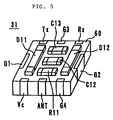
Fig. 3 is a perspective view of the exterior of the high-frequency switch shown
in Fig. 2.
Fig. 4 is an exploded perspective view of a second embodiment of a
high-frequency switch according to the present invention.
Fig. 5 is an external perspective view of the high-frequency switch shown in
Fig. 4.
Fig. 6 is an electrical circuit diagram showing a prior art high-frequency
switch.
DESCRIPTION OF PREFERRED EMBODIMENTS
[Embodiment 1, Fig. 1 to Fig. 3]
Fig. 1 is an electrical circuit diagram showing an example of a high-frequency
switch 21 according to the present invention. The cathode of a diode D11, forming a
switching element, is connected to a transmission terminal Tx. The cathode of the
diode D11 is grounded via a transmission line 12. The transmission line 12 functions
as a choke element. In addition, the anode of the diode D11 connects to an antenna
terminal ANT.
A reception terminal Rx is connected via a transmission line 13 to the antenna
terminal ANT. Moreover, the cathode of a diode D12 connects to the reception
terminal Rx. The anode of the diode D12 connects to the ground via a DC-blocking
capacitor C12. A voltage-control terminal Vc connects via a resistor R11 to an
intermediate connection point between the diode D12 and the capacitor C12. A
control circuit (not shown) is connected to this voltage-control terminal Vc, and
switches the transmission lines of the high-frequency switch 21.
A series circuit, comprising a transmission line 14 and a capacitor C13,
connects to both ends of the diode D11 (between the anode and the cathode). The
transmission line 14 and the capacitor C13 are provided in order to achieve good
isolation when the diode D11 is in the OFF state.
Here, distributed constant lines having a characteristic impedance of more than
40Ω or high-frequency inductors, are used as the transmission lines 12 and 13.
When distributed constant lines are used, the lengths of the transmission lines 12 and
13 are set within a range of greater than λ/12 and less than λ/4 (where λ is the
wavelength of a desired frequency). A distributed constant line or a high-frequency
inductor is also used for the transmission line 14. Furthermore, floating capacitances
Cf1, Cf2, and Cf3 are generated between the terminals Tx, ANT, Rx, and ground, and
can function as bypass capacitors for impedance adjustment.
Next, transmitting and receiving using this high-frequency switch 21 will be
explained. When a positive potential has been applied to the voltage-control terminal
Vc, this potential provides a forward bias voltage for the diodes D11 and D12.
Therefore, the diodes D11 and D12 switch to the ON state. Since direct current is
blocked by the capacitor C12, the voltage supplied to the voltage-control terminal Vc
is applied to the circuit comprising the diodes D11 and D12.
As a result, a transmission signal which has entered the transmission terminal
Tx passes through the diode D11, and is sent to the antenna terminal ANT. At this
time, most of the transmission signal is not sent to the reception terminal Rx. This is
because the self-inductance of the diode D12 in the ON state and the capacitance of
the capacitor C12 resonate in series at the transmission frequency, whereby the
impedance is 0. That is, the transmission lines 12 and 13 operate as a short-stub of
length λ/4, and consequently the transmission terminal Tx and the antenna terminal
ANT are connected, and the reception terminal Rx is grounded.
Furthermore, when the voltage-control terminal Vc is at ground potential, the
diodes D11 and D12 switch OFF. Therefore, there is a cut-off between the
transmission terminal Tx and the antenna terminal ANT, and in addition, there is a
cut-off between the reception terminal Rx and ground. As a result, a received signal
which has entered the antenna terminal ANT is sent through the transmission line 13 to
the reception terminal Rx, and is mostly not transmitted to the transmission terminal
Tx.
In this way, by controlling the bias voltage applied to the voltage-control
terminal Vc, the high-frequency switch 21 is able to switch between the respective
transmission paths of transmitted and received signals.
Moreover, by connecting the cathodes and anodes of the diodes D11 and D12
in the reverse arrangement to that of the cathodes and anodes of the diodes D1 and D2
of the conventional high-frequency switch 1 shown in Fig. 6, the high-frequency
switch 21 can dispense with the large-capacitance and large-scale DC-blocking
capacitor C1 of the conventional high-frequency switch 1. That is, the
high-frequency switch 21 requires only the small-capacitance and small-scale capacitor
C12, connected between the diode D12 and ground on the reception terminal Rx side.
The capacitance of the capacitor C12 is, for instance, 10 pF near 1 GHz, and 3 pF
near 2 GHz. Consequently, the high-frequency switch 21 can be miniaturized.
Furthermore, by adjusting the capacitance of the capacitor C12, the isolation
between the antenna terminal ANT and the reception terminal Rx, which is especially
important when the transmission terminal Tx and the antenna terminal ANT are
connected, can be increased more than in the conventional high-frequency switch.
As a result, it is possible to reduce insertion loss between the transmission terminal Tx
and the antenna terminal ANT.
Moreover, when transmitting (when the diode D12 is in the ON state), the
voltage-control terminal Vc is shorted to ground, and when receiving (when the diode
D12 is in the OFF state), the voltage-controlled terminal Vc is cut-off from the
high-frequency signal by the high impedance of the diode D12, and consequently, it is
possible to achieve a large isolation between the control circuit connected to the
voltage-control terminal Vc and the high-frequency signal.
And, as shown in Fig. 1, a series circuit comprised of a capacitor C13 and a
transmission line 14 may be connected to the diode D11 in parallel. In this case, the
self-inductance of the diode D11 and the inductance of the transmission line 14 form a
parallel resonance circuit. By matching the resonant frequency thereof with the
frequency of the signal, the impedance at the connection point of the diode D11 and
the transmission line 14 is increased when the diode D11 is in the ON state, and
thereby the insertion loss and the reflection loss are reduced. The capacitor C13 is
provided for blocking the direct current via the transmission line 14.''
Next, an example of a laminated-type high-frequency switch having the
electrical circuit shown in Fig. 1 will be explained with reference to Fig. 2 and Fig. 3.
As shown in FIG. 2, the high-frequency switch 31 comprises dielectric sheets 45b
and 45c respectively provided with distributed constant lines 32a, 32b and the like,
dielectric sheets 45d and 45g respectively provided with wide- area ground electrodes
35 and 36, dielectric sheets 45e and 45f respectively provided with distributed
constant lines 33a, 34a and 33b, 34b, a dielectric sheet 45a provided with peer-hole
pads 50a to 54b, etc.
The distributed constant lines 33a and 33b are for instance spiral-shaped, and
are provided on the left side of the sheets 45e and 45f. The extracted portion 42a of
the distributed constant line 33a is exposed on the far side near the left side of the
sheet 45e, and the extracted portion 42b of the distributed constant line 33b is exposed
on the left side of the sheet 45f. The distributed constant lines 33a and 33b are
electrically connected in series via a peer-hole 58, provided in the sheet 45e, and form
the transmission line 12.
The distributed constant lines 34a and 34b are substantially meander-shaped,
and are provided on the right side of the sheets 45e and 45f. The extracted portion
43a of the distributed constant line 34a is exposed in the center on the front side of the
sheet 45e, and the extracted portion 43b of the distributed constant line 34b is exposed
near the right side on the far side of the sheet 45f. The distributed constant lines 34a
and 34b are electrically connected in series via a peer-hole 59, provided in the sheet
45e, and form the transmission line 13.
The distributed constant lines 32a and 32b are spiral-shaped, and are provided
on the right side of the sheets 45b and 45c. The distributed constant lines 32a and
32b are electrically connected in series via a peer-hole 57, provided in the sheet 45b,
and form the transmission line 14. In this way, transmission lines 12 to 14 having
fixed impedance characteristics each comprise two layers and comprise distributed
constant lines 33a, 33b, 34a, 34b, 32a, and 32b, whereby the length of a transmission
line portion on each one layer can be shorter than in the conventional art. Therefore,
the size of the sheets 45a-45g can be reduced, obtaining a high-frequency switch 31
which occupies a small area with respect to a printed circuit substrate or the like.
The ground electrodes 35 and 36 are provided over a wide area on the surfaces
of the sheets 45d and 45g. The extracted portions 35a and 36a of the ground
electrodes 35 and 36 are exposed on the left sides of the sheets 45d and 45g, the
extracted portions 35b and 36b are exposed on the right, the extracted portions 35c
and 36c are exposed in the center on the far sides of the sheets 45d and 45g, and the
extracted portions 35d and 36d are exposed near the right side on the front sides of the
sheets 45d and 45g. The transmission lines 12 and 13 are provided in parallel
between these two ground electrodes 35 and 36.
Moreover, extracted electrodes 37, 38, 39, and a relay electrode 40 are
provided on the surface of the sheet 45b on which the distributed constant line 32a is
provided. Ends of each of the extracted electrodes 37 and 38 are exposed near the
left side and right side on the far side of the sheet 45b, and the end of the extracted
electrode 39 is exposed near the left side on the front side of the sheet 45b. Then,
the distributed constant line 32a is electrically connected to a peer-hole pad 52b, the
extracted electrode 37 is electrically connected to peer- hole pads 50a and 52a, the
extracted electrode 38 is electrically connected to a peer-hole pad 51a, and the relay
electrode 40 is electrically connected to peer- hole pads 53b, 54b, and 51b.
An extracted electrode 41 is provided on the surface of the sheet 45c on which
the distributed constant line 32b is provided. One end of the extracted electrode 41
is exposed in the center of the front side of the sheet 45c. Then, the extracted
electrode 41 is electrically connected to the distributed constant line 32b, and in
addition, electrically connected via the peer-hole 55 to the peer-hole pad 50b.
Furthermore, the peer-hole pad 53a is electrically connected to the ground electrode
5 via the peer-holes 56a and 56b provided in the sheets 45b and 45c.
When all the sheets 45a - 45g having the above constitutions are piled on top
of each other and heat-bonded together, the multilayered body 60 shown in Fig. 3 is
obtained. A transmission terminal Tx, a ground terminal G3, and a reception
terminal Rx are provided on the left side, the center, and the right side of the side face
portion on the far side of the multilayered body 60. A voltage-control terminal Vc,
an antenna terminal ANT, and a ground terminal G4 are provided on the left side, the
center, and the right side of the side face portion on the front side of the multilayered
body 60. Ground terminals G1 and G2 are provided on the left and right side face
portions of the multilayered body 60.
The transmission terminal Tx is electrically connected to one end of the
transmission line 12 (specifically, to the extracted portion 42a of the distributed
constant line 33a), and to the extracted electrode 37. The reception terminal Rx is
electrically connected to one end of the transmission line 13 (specifically, to the
extracted portion 43b of the distributed constant line 34b), and to the extracted
electrode 38. The antenna terminal ANT is electrically connected to the other end of
the transmission line 13 (specifically, to the extracted portion 43a of the distributed
constant line 34a), and to the extracted electrode 41. The voltage-control terminal
Vc is electrically connected to the extracted electrode 39. The ground terminal G1 is
electrically connected to the other end of the transmission line 12 (specifically, the
extracted portion 42b of the distributed constant line 33b), and to the extracted
portions 35a and 36a of the ground electrodes 35 and 36. The ground terminals G2,
G3, and G4 are electrically connected respectively to the extracted portions 35b, 36b,
35c, 36c, 35d, and 36d of the ground electrodes 35 and 36.
Moreover, the cathode electrode and anode electrode of the diode D11 are
soldered to the pads 50a and 50b on the multilayered body 60, the cathode electrode
and anode electrode of the diode D12 are soldered to the pads 51a and 51b, the
terminal electrodes of the capacitor C13 are soldered to the pads 52a and 52b, the
terminal electrodes of the capacitor C12 are soldered to the pads 53a and 53b, and the
terminal electrodes of the resistor R11 are soldered to the pads 54a and 54b.
This obtains a surface mount-type multilayered high-frequency switch 31
having the electrical circuit shown in Fig. 1. This multilayered high-frequency switch
31 does not require a large-capacitance DC-blocking capacitor C1, as in the
conventional high-frequency switch 1 shown in Fig. 6, to be incorporated in or
mounted on the multilayered body 60, and consequently even though the transmission
lines 12 to 14 each comprise two layers, the number of layers in the multilayered body
60 can be reduced. Moreover, the size of the sheets 45a-45g can be reduced,
reducing the area occupied by the high-frequency switch 31 on a printed circuit
substrate or the like.
Furthermore, in the high-frequency switch 1 shown in Fig. 6, a resistor Ra (an
external component) was electrically connected at an intermediate connection point
between the transmission line 2 and the capacitor C1, causing complex
interconnections. By contrast, in the high-frequency switch 31, since one end of the
transmission line 12 connects to the ground terminal G1, interconnection is simple,
thereby enabling the number of layers in the multilayered body 60 to be reduced, and
leading to a consequent improvement in transmission loss by eliminating unnecessary
coupling.
[Embodiment 2, Fig. 4 and Fig. 5]
Another example of a multilayered high-frequency switch having the electrical
circuit shown in Fig. 1 will be explained referring to Fig. 4 and Fig. 5. The
high-frequency switch 61 of this second embodiment contains a DC-blocking
capacitor C12 within its multilayered body. In Figs. 4 and 5, the same parts as those
in Figs. 2 and 3 are represented by the same reference numerals, and explanation
thereof is omitted.
As shown in Fig. 4, the high-frequency switch 61 comprises a dielectric sheet
45j; comprising a distributed constant line 62 and a capacitor electrode 70, dielectric
sheets 45d and 45g comprising wide- area ground electrodes 35 and 36, a dielectric
sheet 45k comprising distributed constant lines 63 and 64, a dielectric sheet 45i;
comprising extracted electrodes 37 and 38 and the like, a dielectric sheet 45h
comprising peer- hole pads 50a and 50b and the like, etc.
The distributed constant line 62 is for instance meander-shaped, and forms a
transmission line 14. One end of the distributed constant line 62 is electrically
connected to the extracted electrode 41, and the other end is electrically connected to
the peer-hole pad 52b via a peer-hole 67, provided in the sheet 45i. The distributed
constant lines 63 and 64 are substantially meander-shaped, and respectively form
transmission lines 12 and 13. One extracted portion 63a of the distributed constant
line 63 is exposed near the left side on the far side of the sheet 45k, and the other
extracted portion 63b is exposed the left side of the sheet 45k. One extracted
portion 64a of the distributed constant line 64 is exposed in the center of the front side
of the sheet 45k, and the other extracted portion 64b is exposed near the right side on
the far side of the sheet 45k. In this way, since the transmission lines 12 to 14 each
comprise one-layer distributed constant lines 63, 64, and 62 respectively, the number
of layers of the multilayered body 80 (explained later) can be further reduced.
The capacitor electrode 70 is formed on the sheet 45j on the side thereof away
from the ground electrode 35, and together with the ground electrode 35 forms a
capacitor C12. The capacitor electrode 70 electrically connects via a peer-hole 66 to
the relay electrode 65 provided on the sheet 45i. Moreover, the relay electrode 65 is
electrically connected to the peer- hole pads 51b and 54b.
When the sheets 45d and 45g-45k of the above constitution are piled on top of
each other and heat-bonded together, the multilayered body 80 as shown in Fig. 5 is
obtained. A transmission terminal Tx, a ground terminal G3, and a reception
terminal Rx are provided on the side face portion at the far side of the multilayered
body 80. A voltage-control terminal Vc, an antenna terminal ANT, and a ground
terminal G4 are provided on the side face portion at the front side of the multilayered
body 80. Ground terminals G1 and G2 are provided on the left and right side face
portions of the multilayered body 80.
The transmission terminal Tx is electrically connected to the extracted portion
63a of the distributed constant line 63, and to the extracted electrode 37. The
reception terminal Rx is electrically connected to the extracted portion 64a of the
distributed constant line 64, and to the extracted electrode 38. The antenna terminal
ANT is electrically connected to the extracted portion 64a of the distributed constant
line 64, and to the extracted electrode 41. The voltage-control terminal Vc is
electrically connected to the extracted electrode 39. The ground terminal G1 is
electrically connected to the extracted portion 63b of the distributed constant line 63,
and to the extracted portions 35a and 36a of the ground electrodes 35 and 36. The
ground terminals G2, G3, and G4 are electrically connected to the extracted portions
35b, 36b, 35c, 36c, 35d, and 36d of the ground electrodes 35 and 36 respectively.
Moreover, the cathode electrode and anode electrode of the diode D11 are
soldered to the pads 50a and 50b on the multilayered body 80, the cathode electrode
and anode electrode of the diode D12 are soldered to the pads 51a and 51b, the
terminal electrodes of the capacitor C13 are soldered to the pads 52a and 52b, and the
terminal electrodes of the resistor R11 are soldered to the pads 54a and 54b.
This obtains a surface mount-type multilayered high-frequency switch 61
having the electrical circuit shown in Fig. 1. Since the capacitor C12 has a small
capacitance, the area of the capacitor electrode 70 is smaller and it occupies less area
when incorporated in the multilayered body 80. Therefore, the high-frequency
switch 61 can be more miniaturized than a conventional one.
Moreover, in the high-frequency switch 61, since the capacitor C12 is
contained in the multilayered body 80, the length of the interconnection from the
capacitor C12 to ground is shorter than when the capacitor C12 is mounted on the
multilayered body as an external component. Therefore, there is less residual
impedance, improving the DC bias-blocking effect. Moreover, the value of the
capacitor C12 can be minutely adjusted by changing the size of the capacitor electrode
70, a greater isolation can be achieved between the antenna terminal ANT and the
reception terminal Rx when the transmission terminal Tx and the antenna terminal
ANT are connected than in a conventional high-frequency switch, and there is a
reduction in insertion loss between the transmission terminal Tx and the antenna
terminal ANT.
[Other Embodiments]
The high-frequency switch according to the present invention is not restricted
to the embodiments described above, and various modifications can be made thereto
within the scope of its main features.
For instance, in the high-frequency switch 21 shown in Fig. 1, the series circuit
comprising the transmission line and the capacitor may be connected to both ends
(between the anode and the cathode) of the diode D12. Alternatively, capacitors
may be connected in parallel to both ends (between the anode and the cathode) of the
diodes D11 and D12, in parallel with the series circuit comprising the transmission line
and the capacitor, improving the isolation when the diodes D11 and D12 are OFF.
Furthermore, resistances (greater than 10KΩ) may be connected in parallel to both
ends of the diodes D11 and D12, in order to stabilize the voltage when a reverse bias
is applied.
Furthermore, in the above embodiments, since a DC bias is applied to the
terminals Tx, Rx, and ANT, a separate coupling capacitor for DC bias-blocking may
be connected to these terminals Tx, Rx and ANT as required.
As is clear from the above explanation, according to the present invention, by
making the direction of the cathode and anode of the diode the reverse of that in a
conventional high-frequency switch, the conventional large-scale and
large-capacitance DC-blocking capacitor connected in the transmission terminal side
becomes unnecessary, and it is only necessary to connect a small-scale and
small-capacitance DC-blocking capacitor in the reception terminal side. Therefore,
the high-frequency switch can be miniaturized.
Furthermore, by adjusting the capacitance of this small-scale capacitor, a
greater isolation between the antenna terminal and the reception terminal can be
obtained than in a conventional high-frequency switch. Therefore, insertion loss
between the transmission terminal and the antenna terminal can be reduced.
Moreover, when transmitting, the voltage-control terminal is shorted to ground, and
when receiving, the voltage-control terminal is cut-off from the high-frequency signal
by the high impedance of a second diode, and consequently, a large isolation can be
achieved between the control circuit connected to the voltage-control terminal and the
high-frequency signal. As a result, it is possible to obtain a high-frequency switch of
superior performance.
While the invention has been particularly shown and described with reference
to preferred embodiments thereof, it will be understood by those skilled in the art that
the foregoing and other changes in form and details may be made therein without
departing from the spirit of the invention.