EP1024521A2 - Process for production of semiconductor device - Google Patents
Process for production of semiconductor device Download PDFInfo
- Publication number
- EP1024521A2 EP1024521A2 EP00101375A EP00101375A EP1024521A2 EP 1024521 A2 EP1024521 A2 EP 1024521A2 EP 00101375 A EP00101375 A EP 00101375A EP 00101375 A EP00101375 A EP 00101375A EP 1024521 A2 EP1024521 A2 EP 1024521A2
- Authority
- EP
- European Patent Office
- Prior art keywords
- semiconductor device
- platinum group
- producing
- group metal
- cleaning
- Prior art date
- Legal status (The legal status is an assumption and is not a legal conclusion. Google has not performed a legal analysis and makes no representation as to the accuracy of the status listed.)
- Withdrawn
Links
Images



Classifications
-
- H—ELECTRICITY
- H10—SEMICONDUCTOR DEVICES; ELECTRIC SOLID-STATE DEVICES NOT OTHERWISE PROVIDED FOR
- H10D—INORGANIC ELECTRIC SEMICONDUCTOR DEVICES
- H10D1/00—Resistors, capacitors or inductors
- H10D1/60—Capacitors
- H10D1/68—Capacitors having no potential barriers
- H10D1/692—Electrodes
-
- H—ELECTRICITY
- H10—SEMICONDUCTOR DEVICES; ELECTRIC SOLID-STATE DEVICES NOT OTHERWISE PROVIDED FOR
- H10P—GENERIC PROCESSES OR APPARATUS FOR THE MANUFACTURE OR TREATMENT OF DEVICES COVERED BY CLASS H10
- H10P52/00—Grinding, lapping or polishing of wafers, substrates or parts of devices
-
- H—ELECTRICITY
- H10—SEMICONDUCTOR DEVICES; ELECTRIC SOLID-STATE DEVICES NOT OTHERWISE PROVIDED FOR
- H10D—INORGANIC ELECTRIC SEMICONDUCTOR DEVICES
- H10D1/00—Resistors, capacitors or inductors
- H10D1/60—Capacitors
- H10D1/68—Capacitors having no potential barriers
- H10D1/682—Capacitors having no potential barriers having dielectrics comprising perovskite structures
-
- H—ELECTRICITY
- H10—SEMICONDUCTOR DEVICES; ELECTRIC SOLID-STATE DEVICES NOT OTHERWISE PROVIDED FOR
- H10P—GENERIC PROCESSES OR APPARATUS FOR THE MANUFACTURE OR TREATMENT OF DEVICES COVERED BY CLASS H10
- H10P70/00—Cleaning of wafers, substrates or parts of devices
- H10P70/10—Cleaning before device manufacture, i.e. Begin-Of-Line process
- H10P70/15—Cleaning before device manufacture, i.e. Begin-Of-Line process by wet cleaning only
-
- H—ELECTRICITY
- H10—SEMICONDUCTOR DEVICES; ELECTRIC SOLID-STATE DEVICES NOT OTHERWISE PROVIDED FOR
- H10P—GENERIC PROCESSES OR APPARATUS FOR THE MANUFACTURE OR TREATMENT OF DEVICES COVERED BY CLASS H10
- H10P70/00—Cleaning of wafers, substrates or parts of devices
- H10P70/20—Cleaning during device manufacture
- H10P70/27—Cleaning during device manufacture during, before or after processing of conductive materials, e.g. polysilicon or amorphous silicon layers
- H10P70/273—Cleaning during device manufacture during, before or after processing of conductive materials, e.g. polysilicon or amorphous silicon layers the processing being a delineation of conductive layers, e.g. by RIE
Definitions
- the present invention relates to a process for production of a semiconductor device, particularly to a process for production of a semiconductor device having a capacitor part comprising electrodes made of a platinum group metal (e.g. platinum or iridium), which process comprises steps of removing the contaminants derived from the platinum group metal.
- a platinum group metal e.g. platinum or iridium
- Memory cells such as DRAM have become increasingly fine in recent years, but it is difficult to allow them to have a sufficient capacity when a conventional nitride or oxide film is used as the dielectric film, because the film has a dielectric constant of only about 2 to 3.
- a ferroelectric film having an ionic bond type perovskite structure composed of barium titanate, strontium titanate, barium strontium titanate or the like.
- ferroelectric random access memory FeRAM
- logic LSI's mounting a ferroelectric random access memory (FeRAM) thereon have come to be widely used in IC cards or general-purpose microcomputers, and ferroelectric films such as PZT (Pb(ZrTi)O 3 ) and SBT (SrBi 2 Ta 2 O 9 ) are in use as the capacitive insulating film of the FeRAM.
- ferroelectric films when in direct contact with the substrate of FeRAM, give rise to oxidation of the substrate and consequent deterioration of FeRAM capacity. Therefore, in using such a ferroelectric film composed of the above material, there has come to be used an upper or lower capacitor electrode composed of a platinum group metal (e.g.
- Fig. 4(a) to Fig. 4(i) are sectional views showing the steps employed in production of a semiconductor memory device which has, in combination, a MOS transistor and a capacitor part comprising platinum group metal electrodes and a ferroelectric film and which can conduct data storage by charge accumulation. Referring to these figures, an example of use of platinum group metal in production of a semiconductor memory device is described specifically.
- a MOS type transistor is formed on a silicon substrate 1 according to a known method, as shown in Fig. 4(a). That is, there is formed a field oxide 2 as an element-isolating region, by a known method such as LOCOS (Local Oxidation of Silicon); subsequently, there is formed a silicon oxide film as a gate-insulating film 3 in a thickness of about 50 to 100 nm, by thermal oxidation. Then, a P-doped polysilicon film and a WSi film are formed in this order; after which they are subjected to patterning to form a gate electrode 4 . Thereafter, ion implantation is conducted to form an impurity-diffused layer 5 , whereby a MOSFET is completed.
- LOCOS Local Oxidation of Silicon
- a boron-containing silicon oxide film (BPSG) as a first inter-layer insulating film 6 ; then, etching is conducted to form a contact hole; in the hole are formed a Ti film and a W film in this order to form a vertical interconnect 7 .
- BPSG boron-containing silicon oxide film
- a platinum thin film which becomes a lower electrode layer 8 of capacitor part there is formed a ferroelectric film 9 (e.g. PZT) and a platinum thin film which becomes an upper electrode layer 10 of capacitor part, in this order.
- ferroelectric film 9 e.g. PZT
- a masking layer 11 consisting of a silicon oxide film is formed in order to protect the above-formed capacitor part at a time when other element part is formed.
- a photoresist pattern 12 is formed on the masking layer 11 , as shown in Fig. 4(e).
- the masking layer 11 , the upper electrode layer 10 , the ferroelectric film 9 and the lower electrode layer 8 are dry-etched to form a desired capacitor part 14 and leave thereon the masking layer 11 , as shown in Fig. 4(f).
- a second inter-layer insulating film 15 is formed so as to cover the capacitor part 14 and the first inter-layer insulating film 6 , as shown in Fig. 4(h); thereafter, there is formed, in the film 15 , an opening 16 for connecting an upper wiring (to be formed later) to the upper electrode layer 10 , as shown in Fig. 4(i).
- a metal film is formed so as to fill the opening 16 and further cover the whole surface of the material obtained in the step of Fig. 4(i); the metal film is subjected to patterning to form a desired upper wiring 17 ; thereon is formed a third inter-layer insulating film 18 (e.g. a silicon nitride film), whereby is formed a semiconductor memory device such as shown in the sectional view of Fig. 3.
- a third inter-layer insulating film 18 e.g. a silicon nitride film
- JP-A-10-12836 discloses a method for removing the etching residue by using, as a cleaning solution, hydrochloric acid, nitric acid, hydrofluoric acid, a mixture thereof, water of 80°C or higher temperature, or an organic solvent.
- a silicon oxide film as a protective mask 11 for formation of other element part, or a second inter-layer insulating film 15 so as to cover a capacitor part 14 platinum atoms or particles 13 are generated from the upper platinum thin film 10 of the capacitor part 14 and deposit on the protective mask 11 or the second inter-layer insulating film 15 ; when there is formed a contact hole communicating with the upper electrode, there adhere, onto the second inter-layer insulating film 15 , the platinum atoms or particles vaporized from the upper platinum thin film, a reaction product thereof with chlorine gas (a dry-etching gas), i.e.
- chlorine gas a dry-etching gas
- Such contaminants include (1) a metal ion adsorbed by or bonded with the surface of a semiconductor substrate, the surface of an insulating film (e.g. a silicon oxide film) formed thereon, and the back surface of the substrate, and (2) metal particles adhering thereon.
- an insulating film e.g. a silicon oxide film
- one cleaning tank is used for a plurality of cleaning steps, depending upon the kind of the target substance to be removed.
- one cleaning tank used for cleaning of a substrate contaminated with a platinum group metal is used for cleaning of other substrate, secondary contamination may take place. Therefore, the contamination of the former substrate by platinum group metal need be removed beforehand.
- Use of one apparatus for a contaminated substrate and other substrate may be also conducted in various steps such as, oxide film formation step in addition to the above-mentioned cleaning step.
- HCl-H 2 O 2 -H 2 O: HPM hydrochloric acid, hydrogen peroxide and water
- SPM sulfuric acid and hydrogen peroxide
- aqua regia mixed solution of nitric acid and hydrochloric acid
- ammonia water, hydrogen peroxide and water NH 4 OH-H 2 O 2 -H 2 O: APM
- These techniques are effective for removal of ordinary metal contaminants but make no suggestion to contamination by platinum group metals such Pt and Ir.
- JP-A-7-45580 is disclosed a technique of removing metal contaminants such copper adhering onto the surface of wafer, by a series of cleaning steps which comprise first removing a natural oxide present on a silicon wafer with dilute hydrofluoric acid, then treating the resulting wafer with a mixture of hydrofluoric acid, hydrochloric acid, hydrogen peroxide and water, and thereafter cleaning with a mixture of hydrochloric acid, hydrogen peroxide and water.
- the platinum group metals such as platinum and iridium are stable to hydrofluoric acid. Therefore, when treatment with hydrofluoric acid is conducted first, the contaminants adhering onto the oxide film surface, etc. are detached and transferred into the treating solution simultaneously with the etching of the oxide film but are present in the solution as a suspending component. Therefore, they readhere onto the substrate when it is taken out of the solution and cannot be removed sufficiently.
- JP-A-6-333898 is disclosed a technique of cleaning the surface of a semiconductor substrate using a cleaning solution containing (1) a strong acid and an oxidizing agent for removing the organic substances and inorganic substances remaining on the surface of the semiconductor substrate, (2) a fluorine-containing compound consisting of fluorine-generating fluorosulfuric acid or sulfuryl difluoride, for removing the residue and particles which remain on the surface of the semiconductor substrate when the surface is subjected to very slight etching, and (3) water.
- a cleaning solution containing (1) a strong acid and an oxidizing agent for removing the organic substances and inorganic substances remaining on the surface of the semiconductor substrate, (2) a fluorine-containing compound consisting of fluorine-generating fluorosulfuric acid or sulfuryl difluoride, for removing the residue and particles which remain on the surface of the semiconductor substrate when the surface is subjected to very slight etching, and (3) water.
- a cleaning solution containing (1) a strong acid and an oxidizing agent for
- the present inventor proposed, in order to remove the contamination by a platinum group metal, of an insulating film formed on a semiconductor substrate, a technique of removing the platinum group metal using a cleaning solution which is a mixture of (1) a chemical solution for metal removal and (2) a very small amount of hydrofluoric acid.
- a cleaning solution which is a mixture of (1) a chemical solution for metal removal and (2) a very small amount of hydrofluoric acid.
- the hypochlorous acid ion or sulfuric acid ion formed in the cleaning system ionizes the platinum group metal and makes it soluble; thereby, the readhesion of the platinum group metal is prevented; thus, the contamination by platinum group metal can be reduced to less than 1 x 10 10 atoms/cm 2 .
- the object of the present invention lies in providing (1) a cleaning solution which can reliably remove the contaminants derived from a platinum group metal (e.g. Pt or Ir), adhering onto the silicon-based insulating film (e.g. silicon oxide film) formed on a silicon substrate or onto the back surface of the silicon substrate and which further can prevent the readhesion of the removed contaminants; and (2) a cleaning method using said cleaning solution.
- a cleaning solution which can reliably remove the contaminants derived from a platinum group metal (e.g. Pt or Ir), adhering onto the silicon-based insulating film (e.g. silicon oxide film) formed on a silicon substrate or onto the back surface of the silicon substrate and which further can prevent the readhesion of the removed contaminants.
- the present inventor made an intensive study in order to achieve the above object. As a result, it was found out that when a cleaning solution consisting of a chemical solution for metal removal and very small amounts of hydrofluoric acid and a chelating agent is sued in order to remove the contaminants derived from a platinum group metal, adhering onto (1) the insulating film formed on a semiconductor substrate and (2) the back surface of the substrate, the contaminants can be removed reliably and the removed contaminants react with the chelating agent and do not readhere.
- a cleaning solution consisting of a chemical solution for metal removal and very small amounts of hydrofluoric acid and a chelating agent is sued in order to remove the contaminants derived from a platinum group metal, adhering onto (1) the insulating film formed on a semiconductor substrate and (2) the back surface of the substrate.
- the present invention lies in a process for producing, starting from a silicon substrate, a semiconductor device having a capacitor part comprising platinum group metal electrodes and a ferroelectric film, which process comprises a cleaning step of cleaning and removing the platinum group metal-derived contaminants adhering onto (1) the silicon-based insulating film formed in contact with the platinum group metal of the electrode(s) and (2) the back surface of the silicon substrate, by using a cleaning solution comprising a chemical solution for metal removal and very small amounts of hydrofluoric acid and a chelating agent.
- the contaminants derived from a platinum group metal can be removed reliably; the removed contaminants do not readhere, and secondary contamination in other device can be prevented. Further, in the present invention, since the back surface of a substrate is cleaned to remove the platinum group metal-derived contaminants after the formation or etching of a platinum group metal film, when the resulting substrate is transferred, by the use of a handler, to a next-step apparatus, for example, a CVD apparatus for silicon oxide film formation, the handler is not contaminated by the platinum group metal. As a result, it does not happen that other semiconductor substrate is cross-contaminated by the platinum group metal.
- Formation of an inter-layer insulating film or the like on an exposed platinum group metal layer results in contamination of the surface of the formed inter-layer insulating film by the platinum group metal ion vaporized during the above formation.
- the thus-generated platinum group metal contaminants can be removed by dipping the substrate after the above formation in a cleaning solution to clean the principal and back surfaces of the substrate.
- the cleaning solution contains a chelating agent, the concentration of hydrochloric acid in the cleaning solution can be made low; thereby, the adverse effect of cleaning on element part can be reduced.
- the chemical solution for metal removal used in the present invention, there can be mentioned a solution comprising an inorganic acid (e.g. hydrochloric acid or sulfuric acid) and hydrogen peroxide.
- an inorganic acid e.g. hydrochloric acid or sulfuric acid
- hydrogen peroxide e.g. hydrochloric acid or sulfuric acid
- hydrochloric acid is preferred.
- a platinum group metal can be removed at a high efficiency when there is used a cleaning solution containing (1) components (e.g. a combination of hydrochloric acid and hydrogen peroxide) capable of generating hypochlorous acid in a cleaning system and (2) a small amount, preferably 1 wt% or less of hydrofluoric acid.
- An aqueous hypochlorous acid solution is very unstable and is ordinarily available in the form of a hypochlorite (e.g. sodium or potassium salt).
- the hypochlorite is unusable because it contains a cation (e.g. Na ion or K ion) which adversely affects the elements of semiconductor device.
- use of unstable hypochlorous acid has been made possible by using, in combination, the components capable of generating hypochlorous acid in the cleaning system.
- This hypochlorous acid reacts with a platinum group metal (e.g. Pt or Ir) as contaminant to convert the metal, directly or via its chloride (e.g. platinum chloride or iridium chloride), into tetrachloroplatinic acid ion (H[PtCl 4 ] - ) or tetrachloroiridic acid ion (H[IrCl 4 ] - ), thereby, the amount of contaminant (platinum group metal) remaining as a suspending component in the cleaning solution becomes small.
- a platinum group metal e.g. Pt or Ir
- the cleaning solution of the present invention further contains a chelating agent, the platinum group metal remaining in the cleaning solution is reacted with the chelating agent and converted into a chelate; as a result, substantially no suspending component remains in the cleaning solution and readhesion of contaminant can be prevented reliably.
- the hydrofluoric acid also contained in the cleaning solution etches a silicon-based insulating film, whereby the platinum group metal-derived contaminants adhering onto the silicon-based insulating film can be removed easily.
- the chelating agent used in the present invention can be any chelating agent capable of forming a chelate with a platinum group metal. However, it is preferably a dibasic carboxylic acid because the acid is stable to the chemical solution for metal removal used together.
- dibasic carboxylic acid there can be mentioned aliphatic dibasic carboxylic acids such as oxalic acid, malonic acid, succinic acid, citric acid, malic acid, fumaric acid, citraconic acid and tartaric acid; and aromatic dibasic carboxylic acids such as phthalic acid and naphthal acid. Besides these carboxylic acids, there can also be used polybasic carboxylic acids such as pyromellitic acid.
- the amount of the chelating agent used is about 100 ppm to 1% by weight, and a sufficient effect can be obtained with this amount.
- the contamination level is reduced to less than 1x10 10 atoms/cm 2 and a sufficient effect is obtained.
- a chelating agent is added to HPFM or SPFM, the Pt contamination can be removed to nearly the detection limit.
- the treatment was conducted at 65°C (the temperature of cleaning solution) when the cleaning solution was a hydrochloric acid type, and at 130°C when the cleaning solution was a sulfuric acid type.
- the measurement of the Pt contamination level was made by wafer surface treatment using hot aqua regia recovering solution and subsequent ICP-MS measurement; in this case, the detection limit is about 1x10 9 atoms/cm 2 .
- Hydrochloric acid can be used in a concentration of 1 to 25% by weight.
- a concentration of 1 to 10% by weight is preferred in view of the adverse effect on other element part.
- Hydrogen peroxide is preferably used in a concentration of about 0.5 to 5% by weight. When the concentration of hydrochloric acid is low, the concentration of hydrogen peroxide is preferred to be correspondingly low.
- the amount of hydrofluoric acid used can be determined so as to become optimum relative to the etching rate of silicon oxide film, but is preferably 1% by weight or less.
- the amount can be larger than that when there is etched a silicon-based insulating film other than silicon oxide film, such as silicon nitride film or silicon oxide nitride film.
- the amount of hydrofluoric acid is determined so that the etching rate becomes 1 to 5 nm/min.
- the cleaning solution of the present invention similarly to conventional cleaning solutions containing hydrogen peroxide, has no sufficiently long life. Therefore, it is desired that hydrogen peroxide be mixed with other components of the present cleaning solution right before the use of the cleaning solution.
- the cleaning solution is used in cleaning operation at a temperature of room temperature (25°C) solution, preferably at a temperature of about 50 to 70°C.
- the cleaning time can be appropriately varied depending upon the amounts of hydrochloric acid and hydrogen peroxide, the use temperature of cleaning solution, etc.
- the cleaning time is ordinarily about 1 to 15 minutes, preferably about 5 to 10 minutes.
- the contaminants on the back surface of a substrate can be easily removed by, prior to formation of a platinum group metal layer, forming a thin oxide film layer on the back surface of the substrate. Since platinum group metal-derived contaminants are adsorbed more easily by silicon than by silicon oxide film, the above formation of a thin oxide film layer on the back surface of the substrate is effective.
- the thin oxide film layer can be formed by a known method such as thermal oxidation or chemical vapor deposition (CVD), and the thickness of the film can be about 10 to 100 nm.
- the cleaning operation can be conducted by dipping a whole operation can be conducted by dipping a whole substrate including elements in a cleaning solution; or, after formation of an element part on a substrate, by contacting only the back surface of the substrate with a cleaning solution.
- the cleaning operation may also be conducted by other known method such as spraying or cleaning with running water.
- Fig. 2(a) to Fig. 2(g) are sectional views showing steps employed in production of a semiconductor memory device which has, in combination, a MOS transistor and a capacitor part comprising platinum group metal electrodes and a ferroelectric film and which can conduct data storage by charge accumulation.
- a MOS type transistor is formed on a silicon substrate 1 according to a known method, as shown in Fig. 2(a). That is, there is formed a field oxide 2 as an element-isolating region, by a known method such as LOCOS; subsequently, there is formed a silicon oxide film as a gate-insulating film 3 in a thickness of about 50 to 100 nm, by thermal oxidation. Then, a P-doped polysilicon film and a WSi film are formed in this order; after which they are subjected to patterning to form a gate electrode 4 . Thereafter, ion implantation is conducted to form an impurity-diffused layer 5 , whereby a MOSFET is completed.
- a BPSG film as a first inter-layer insulating film 6 ; then, etching is conducted to form a contact hole; in the hole are formed a Ti film and a W film in this order to form a vertical interconnect 7 .
- a platinum thin film which becomes a lower electrode layer 8 of capacitor part there is formed a platinum thin film which becomes a lower electrode layer 8 of capacitor part; then, there are formed, by sputtering, a ferroelectric film 9 (e.g. PZT) and a platinum or iridium thin film which becomes an upper electrode layer 10 of capacitor part, in this order.
- a ferroelectric film 9 e.g. PZT
- platinum or iridium thin film which becomes an upper electrode layer 10 of capacitor part
- a masking layer 11 consisting of a silicon oxide film is formed by CVD in order to protect the above-formed capacitor part at a time when other element part is formed.
- platinum-derived contaminants 13 adhere onto the masking layer 11 and the back surface of the substrate 1 .
- the contaminants 13 are presumed to be adhered by release of platinum ion from thin platinum film present on wafer, during formation of silicon oxide film by CVD, or by scattering of contaminants adhering onto the back surface of wafer when there is no cleaning of the back surface in the previous step. This fact that platinum-derived contaminants adhere onto the surface of silicon oxide film in a step other than formation of platinum thin film or etching of platinum thin film, was newly found out by the present inventor. If a next step is conducted without removing platinum-derived contaminants formed in this step, the contaminants diffuse in the wafer or are transferred onto other wafer, whereby the properties of elements are affected adversely.
- the substrate contaminated with platinum is dipped in the cleaning solution of the present invention and subjected to a cleaning operation.
- the composition of cleaning solution and conditions of cleaning used in the cleaning operation are as follows.
- Hydrochloric acid 5% by weight Hydrogen peroxide 4% by weight Hydrofluoric acid 0.1% by weight Chelating agent (oxalic acid) 1000 ppm Water Remainder
- a photoresist pattern is formed on the masking layer 11 ; using this resist pattern as a mask, dry etching is conducted for the masking layer 11 , the capacitor upper electrode layer 10 , the ferroelectric film 9 and the capacitor lower electrode layer 8 to form a desired capacitor part 14 , and the masking layer remaining on the capacitor part 14 is removed [see Fig. 2(e)]. At this time, an etching residue may adhere, but it can be removed by a known method or using the cleaning solution of the present invention.
- a second inter-layer insulating film 15 is formed so as to cover the capacitor part 14 and the first inter-layer insulating film 6 .
- a metal ion is released from the platinum group metal layer of capacitor part and contaminants adhere onto the second inter-layer insulating film and the back surface of substrate. These contaminants can be removed by conducting the same cleaning operation as mentioned above.
- an opening 16 for connecting an upper wiring (to be formed later) to the capacitor upper electrode layer 10 is formed in the second inter-layer insulating film 15 , as shown in Fig. 2(g).
- the exposed upper electrode layer 10 may be etched slightly and there may appear contamination.
- the substrate since the upper electrode is exposed, only the back surface of substrate is cleaned by spraying, cleaning with running water, or the like.
- a metal film is formed so as to fill the opening 16 and further cover the whole surface of the material obtained in the step of Fig. 2(g); the metal film is subjected to patterning in a desired shape to form an upper wiring 17 ; thereon is formed a third inter-layer insulating film 18 (e.g. a silicon nitride film), whereby is formed a semiconductor memory device having a ferroelectric capacitor containing platinum electrodes, such as shown in the sectional view of Fig. 3.
- the back surface of substrate is cleaned and a third inter-layer insulting film 18 is formed, after which the wafer is cleaned by dipping.
Landscapes
- Cleaning Or Drying Semiconductors (AREA)
- Semiconductor Memories (AREA)
Abstract
A process for producing, starting from a
silicon substrate, a semiconductor device having a
capacitor part comprising platinum group metal
electrodes and a ferroelectric film, which process
comprises a cleaning step of cleaning and removing
the platinum group metal-derived contaminants
adhering onto (1) the silicon-based insulating film
formed in contact with the platinum group metal of
the electrode(s) and (2) the back surface of the
silicon substrate, by using a cleaning solution
comprising a chemical solution for metal removal and
very small amounts of hydrofluoric acid and a
chelating agent. This process can remove platinum
group metal-derived contaminants reliably and can
prevent the readhesion of the once-removed
contaminants.
Description
- The present invention relates to a process for production of a semiconductor device, particularly to a process for production of a semiconductor device having a capacitor part comprising electrodes made of a platinum group metal (e.g. platinum or iridium), which process comprises steps of removing the contaminants derived from the platinum group metal.
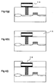
- Memory cells such as DRAM have become increasingly fine in recent years, but it is difficult to allow them to have a sufficient capacity when a conventional nitride or oxide film is used as the dielectric film, because the film has a dielectric constant of only about 2 to 3. In order to solve this problem, there has come to be used a ferroelectric film having an ionic bond type perovskite structure composed of barium titanate, strontium titanate, barium strontium titanate or the like. Also, logic LSI's mounting a ferroelectric random access memory (FeRAM) thereon have come to be widely used in IC cards or general-purpose microcomputers, and ferroelectric films such as PZT (Pb(ZrTi)O3) and SBT (SrBi2Ta2O9) are in use as the capacitive insulating film of the FeRAM. These ferroelectric films, when in direct contact with the substrate of FeRAM, give rise to oxidation of the substrate and consequent deterioration of FeRAM capacity. Therefore, in using such a ferroelectric film composed of the above material, there has come to be used an upper or lower capacitor electrode composed of a platinum group metal (e.g. platinum or iridium) which is non-reactive to the material of ferroelectric film. Fig. 4(a) to Fig. 4(i) are sectional views showing the steps employed in production of a semiconductor memory device which has, in combination, a MOS transistor and a capacitor part comprising platinum group metal electrodes and a ferroelectric film and which can conduct data storage by charge accumulation. Referring to these figures, an example of use of platinum group metal in production of a semiconductor memory device is described specifically.
- First, a MOS type transistor is formed on a
silicon substrate 1 according to a known method, as shown in Fig. 4(a). That is, there is formed afield oxide 2 as an element-isolating region, by a known method such as LOCOS (Local Oxidation of Silicon); subsequently, there is formed a silicon oxide film as a gate-insulatingfilm 3 in a thickness of about 50 to 100 nm, by thermal oxidation. Then, a P-doped polysilicon film and a WSi film are formed in this order; after which they are subjected to patterning to form agate electrode 4. Thereafter, ion implantation is conducted to form an impurity-diffusedlayer 5, whereby a MOSFET is completed. - Next, as shown in Fig. 4(b), there is formed, by CVD, a boron-containing silicon oxide film (BPSG) as a first inter-layer
insulating film 6; then, etching is conducted to form a contact hole; in the hole are formed a Ti film and a W film in this order to form avertical interconnect 7. - Subsequently, as shown in Fig. 4(c), there is formed a platinum thin film which becomes a
lower electrode layer 8 of capacitor part; then, there are formed a ferroelectric film 9 (e.g. PZT) and a platinum thin film which becomes anupper electrode layer 10 of capacitor part, in this order. - Next, as shown in Fig. 4(d), a
masking layer 11 consisting of a silicon oxide film is formed in order to protect the above-formed capacitor part at a time when other element part is formed. - After the other element part has been formed, a
photoresist pattern 12 is formed on themasking layer 11, as shown in Fig. 4(e). Using this resist pattern as a mask, themasking layer 11, theupper electrode layer 10, theferroelectric film 9 and thelower electrode layer 8 are dry-etched to form a desired capacitor part 14 and leave thereon themasking layer 11, as shown in Fig. 4(f). - Next, the
masking layer 11 is removed, as shown in Fig. 4(g). Then, a second inter-layer insulating film 15 is formed so as to cover the capacitor part 14 and the first inter-layerinsulating film 6, as shown in Fig. 4(h); thereafter, there is formed, in the film 15, an opening 16 for connecting an upper wiring (to be formed later) to theupper electrode layer 10, as shown in Fig. 4(i). - Lastly, a metal film is formed so as to fill the opening 16 and further cover the whole surface of the material obtained in the step of Fig. 4(i); the metal film is subjected to patterning to form a desired upper wiring 17; thereon is formed a third inter-layer insulating film 18 (e.g. a silicon nitride film), whereby is formed a semiconductor memory device such as shown in the sectional view of Fig. 3.
- In the steps of Fig. 4, in conducting etching to form a capacitor part 14 having a masking layer thereon, there was a fear that the etching residue adhered to the side wall of the capacitor part 14, resulting in the reduced property of the device produced. To remove the etching residue, a cleaning operation has been carried out. For example, JP-A-10-12836 discloses a method for removing the etching residue by using, as a cleaning solution, hydrochloric acid, nitric acid, hydrofluoric acid, a mixture thereof, water of 80°C or higher temperature, or an organic solvent.
- In production of a semiconductor memory device, when there is formed, as mentioned above, for example, a silicon oxide film as a
protective mask 11 for formation of other element part, or a second inter-layer insulating film 15 so as to cover a capacitor part 14, platinum atoms or particles 13 are generated from the upper platinumthin film 10 of the capacitor part 14 and deposit on theprotective mask 11 or the second inter-layer insulating film 15; when there is formed a contact hole communicating with the upper electrode, there adhere, onto the second inter-layer insulating film 15, the platinum atoms or particles vaporized from the upper platinum thin film, a reaction product thereof with chlorine gas (a dry-etching gas), i.e. platinum chloride, and an oxide thereof; further, they adhere even onto the back surface of asilicon substrate 1. Since the platinum atoms, in particular, easily cause thermal diffusion in the silicon substrate, the platinum atoms adhering onto the back surface of the substrate may move to the transistor element region of semiconductor device; this affects a serious problem on the property of the element. A similar problem arises also when, in forming an insulating film on other silicon substrate for production of a semiconductor device by using the apparatus used for formation of the above-mentioned protective mask or second inter-layer insulating film, the platinum atoms or particles remaining in the apparatus adhere onto the insulating film formed on the other silicon substrate or onto the back surface of the other silicon substrate. It is known that the above remaining of platinum contaminants, even if the amount is as small as about 1 x 10¹⁰ atoms/cm2, adversely affects the life time or electrical property of the semiconductor device produced. - Such contaminants include (1) a metal ion adsorbed by or bonded with the surface of a semiconductor substrate, the surface of an insulating film (e.g. a silicon oxide film) formed thereon, and the back surface of the substrate, and (2) metal particles adhering thereon.
- It is necessary, therefore, to remove such contamination by platinum group metal. However, there has been developed almost no effective methods for removing the contamination.
- In practical production of a semiconductor device, there is a case that one cleaning tank is used for a plurality of cleaning steps, depending upon the kind of the target substance to be removed. In such a case, if one cleaning tank used for cleaning of a substrate contaminated with a platinum group metal is used for cleaning of other substrate, secondary contamination may take place. Therefore, the contamination of the former substrate by platinum group metal need be removed beforehand. Use of one apparatus for a contaminated substrate and other substrate may be also conducted in various steps such as, oxide film formation step in addition to the above-mentioned cleaning step.
- As the conventional chemical solutions for metal removal, there are known, for example, a mixed solution of hydrochloric acid, hydrogen peroxide and water (HCl-H2O2-H2O: HPM); a mixed solution of sulfuric acid and hydrogen peroxide (H2SO4-H2O2: SPM); a mixed solution of nitric acid and hydrochloric acid (aqua regia); and a mixed solution of ammonia water, hydrogen peroxide and water (NH4OH-H2O2-H2O: APM). These conventional chemical solutions for metal removal, however, are used for ordinary heavy metals and are unable to sufficiently remove contaminants such as platinum and iridium having a very low ionization tendency, and are difficult to reduce the contamination level to less than 1x10¹⁰ atoms/cm2 mentioned above. Even if the contaminants are removed from the substrate surface, the removed contaminants are suspended in the cleaning solution used and, therefore, they readhere onto the substrate when the substrate is pulled up from the cleaning solution; after all, the contaminants are difficult to remove.
- Techniques of removing a metal from the surface of silicon wafer or removing contaminants from the surface natural oxide of silicon wafer, by using a mixed solution of hydrochloric acid, hydrofluoric acid and aqueous hydrogen peroxide for cleaning of silicon wafer, are disclosed in, for example, JP-A-3-228327 and JP-A-8-31781. Any of these techniques is for removal of contaminants present on silicon wafer and is applied before various elements of device are formed. A technique of removing contaminants at normal temperature using a mixture of HF:HCl:H2O2:H2 = 1:10:20:100 is disclosed in JP-A-3-228327; and a technique of removing contaminants using a solution obtained by diluting 17% HCl : 25% HF = 1:1 100-fold with water and adding H2O2 thereto is disclosed in JP-A-8-31781. These techniques are effective for removal of ordinary metal contaminants but make no suggestion to contamination by platinum group metals such Pt and Ir.
- In JP-A-7-45580 is disclosed a technique of removing metal contaminants such copper adhering onto the surface of wafer, by a series of cleaning steps which comprise first removing a natural oxide present on a silicon wafer with dilute hydrofluoric acid, then treating the resulting wafer with a mixture of hydrofluoric acid, hydrochloric acid, hydrogen peroxide and water, and thereafter cleaning with a mixture of hydrochloric acid, hydrogen peroxide and water.
- The platinum group metals such as platinum and iridium are stable to hydrofluoric acid. Therefore, when treatment with hydrofluoric acid is conducted first, the contaminants adhering onto the oxide film surface, etc. are detached and transferred into the treating solution simultaneously with the etching of the oxide film but are present in the solution as a suspending component. Therefore, they readhere onto the substrate when it is taken out of the solution and cannot be removed sufficiently.
- In JP-A-6-333898 is disclosed a technique of cleaning the surface of a semiconductor substrate using a cleaning solution containing (1) a strong acid and an oxidizing agent for removing the organic substances and inorganic substances remaining on the surface of the semiconductor substrate, (2) a fluorine-containing compound consisting of fluorine-generating fluorosulfuric acid or sulfuryl difluoride, for removing the residue and particles which remain on the surface of the semiconductor substrate when the surface is subjected to very slight etching, and (3) water. In the Examples of the literature is shown a case of removing the residue adhering after the dry etching of polysilicon film. However, no mention is made on the removal of platinum group metal.
- In Japanese Patent Application No. 10-263482, the present inventor proposed, in order to remove the contamination by a platinum group metal, of an insulating film formed on a semiconductor substrate, a technique of removing the platinum group metal using a cleaning solution which is a mixture of (1) a chemical solution for metal removal and (2) a very small amount of hydrofluoric acid. According to the above technique, the hypochlorous acid ion or sulfuric acid ion formed in the cleaning system ionizes the platinum group metal and makes it soluble; thereby, the readhesion of the platinum group metal is prevented; thus, the contamination by platinum group metal can be reduced to less than 1 x 10¹⁰ atoms/cm2.
- Since a fairly strongly acidic condition is required in order to achieve sufficient removal of contaminants, the above technique may produce an adverse effect depending upon the kind of the semiconductor device produced. Moreover, with the hypochlorous acid ion or sulfuric acid ion alone, although the contaminants on oxide film can be removed, readhesion of the removed contaminants cannot be sufficiently prevented.
- The object of the present invention lies in providing (1) a cleaning solution which can reliably remove the contaminants derived from a platinum group metal (e.g. Pt or Ir), adhering onto the silicon-based insulating film (e.g. silicon oxide film) formed on a silicon substrate or onto the back surface of the silicon substrate and which further can prevent the readhesion of the removed contaminants; and (2) a cleaning method using said cleaning solution.
- The present inventor made an intensive study in order to achieve the above object. As a result, it was found out that when a cleaning solution consisting of a chemical solution for metal removal and very small amounts of hydrofluoric acid and a chelating agent is sued in order to remove the contaminants derived from a platinum group metal, adhering onto (1) the insulating film formed on a semiconductor substrate and (2) the back surface of the substrate, the contaminants can be removed reliably and the removed contaminants react with the chelating agent and do not readhere. The above finding has led to the completion of the present invention.
- The present invention lies in a process for producing, starting from a silicon substrate, a semiconductor device having a capacitor part comprising platinum group metal electrodes and a ferroelectric film, which process comprises a cleaning step of cleaning and removing the platinum group metal-derived contaminants adhering onto (1) the silicon-based insulating film formed in contact with the platinum group metal of the electrode(s) and (2) the back surface of the silicon substrate, by using a cleaning solution comprising a chemical solution for metal removal and very small amounts of hydrofluoric acid and a chelating agent.
- According to the present invention, the contaminants derived from a platinum group metal can be removed reliably; the removed contaminants do not readhere, and secondary contamination in other device can be prevented. Further, in the present invention, since the back surface of a substrate is cleaned to remove the platinum group metal-derived contaminants after the formation or etching of a platinum group metal film, when the resulting substrate is transferred, by the use of a handler, to a next-step apparatus, for example, a CVD apparatus for silicon oxide film formation, the handler is not contaminated by the platinum group metal. As a result, it does not happen that other semiconductor substrate is cross-contaminated by the platinum group metal.
- Formation of an inter-layer insulating film or the like on an exposed platinum group metal layer results in contamination of the surface of the formed inter-layer insulating film by the platinum group metal ion vaporized during the above formation. In the present invention, however, the thus-generated platinum group metal contaminants can be removed by dipping the substrate after the above formation in a cleaning solution to clean the principal and back surfaces of the substrate.
- Moreover, in the present invention, since the cleaning solution contains a chelating agent, the concentration of hydrochloric acid in the cleaning solution can be made low; thereby, the adverse effect of cleaning on element part can be reduced.
- By thus removing the platinum group metal-derived contaminants, there can be eliminated the diffusion of platinum group metal into semiconductor substrate and consequent deterioration of properties of elements such as transistor, whereby a highly reliable semiconductor device can be produced.
-
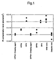
- Fig. 1 is a graph showing the levels of remaining Pt contamination when cleaning solutions of the present invention or conventional techniques were used.
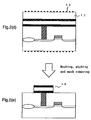
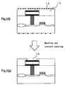
- Fig. 2(a) to Fig. 2(g) are sectional views of steps showing an embodiment of the process for production of a semiconductor device according to the present invention.
- Fig. 3 is a schematic sectional view showing an example of a semiconductor memory device produced by the present invention or a conventional process, which device has, in combination, a MOS transistor and a capacitor part comprising platinum group metal electrodes and a ferroelectric film and which can conduct data storage by charge accumulation.
- Fig. 4(a) to Fig. 4(i) are sectional views of steps showing an example of a conventional process for production of a semiconductor device.
-
- The present invention is hereinafter described in detail.
- As the chemical solution for metal removal, used in the present invention, there can be mentioned a solution comprising an inorganic acid (e.g. hydrochloric acid or sulfuric acid) and hydrogen peroxide. As the inorganic acid, hydrochloric acid is preferred.
- According to the investigation by the present inventor, it was found out that a platinum group metal can be removed at a high efficiency when there is used a cleaning solution containing (1) components (e.g. a combination of hydrochloric acid and hydrogen peroxide) capable of generating hypochlorous acid in a cleaning system and (2) a small amount, preferably 1 wt% or less of hydrofluoric acid. An aqueous hypochlorous acid solution is very unstable and is ordinarily available in the form of a hypochlorite (e.g. sodium or potassium salt). The hypochlorite, however, is unusable because it contains a cation (e.g. Na ion or K ion) which adversely affects the elements of semiconductor device. In the present invention, use of unstable hypochlorous acid has been made possible by using, in combination, the components capable of generating hypochlorous acid in the cleaning system.
- Hydrochloric acid and hydrogen peroxide react with each other to generate hypochlorous acid. This hypochlorous acid reacts with a platinum group metal (e.g. Pt or Ir) as contaminant to convert the metal, directly or via its chloride (e.g. platinum chloride or iridium chloride), into tetrachloroplatinic acid ion (H[PtCl4]-) or tetrachloroiridic acid ion (H[IrCl4]-), thereby, the amount of contaminant (platinum group metal) remaining as a suspending component in the cleaning solution becomes small. Since the cleaning solution of the present invention further contains a chelating agent, the platinum group metal remaining in the cleaning solution is reacted with the chelating agent and converted into a chelate; as a result, substantially no suspending component remains in the cleaning solution and readhesion of contaminant can be prevented reliably.
- At this time, the hydrofluoric acid also contained in the cleaning solution etches a silicon-based insulating film, whereby the platinum group metal-derived contaminants adhering onto the silicon-based insulating film can be removed easily.
- The chelating agent used in the present invention can be any chelating agent capable of forming a chelate with a platinum group metal. However, it is preferably a dibasic carboxylic acid because the acid is stable to the chemical solution for metal removal used together.
- As the dibasic carboxylic acid, there can be mentioned aliphatic dibasic carboxylic acids such as oxalic acid, malonic acid, succinic acid, citric acid, malic acid, fumaric acid, citraconic acid and tartaric acid; and aromatic dibasic carboxylic acids such as phthalic acid and naphthal acid. Besides these carboxylic acids, there can also be used polybasic carboxylic acids such as pyromellitic acid.
- The amount of the chelating agent used is about 100 ppm to 1% by weight, and a sufficient effect can be obtained with this amount.
- Fig. 1 is a graph showing the levels of remaining Pt contamination when the Pt contaminants adhering onto (1) a silicon oxide film formed in a thickness of about 200 nm by CVD and (2) the back surface of a silicon substrate were removed using the cleaning solutions of the present invention or conventional techniques. Shown in Fig. 1 are the Pt atoms adhering per unit area, measured for 2 to 4 wafers. As appreciated from Fig. 1, when a substrate having an initial Pt contamination level of about 1x10¹¹-12 atoms/cm2 is treated with conventional HPM (HCl:H2O2:H2O = 1:1:5) or conventional SPM (H2SO4:H2O2 = 4:1), substantially no contaminant removal takes place. In contrast, when the treatment is made with HPFM (HCl:H2O2:H2O = 3:1:5 + 0.1 wt. % HF) or SPFM (H2SO4:H2O2 = 4:1 + 0.1 wt. % HF), previously proposed by the present inventor, the contamination level is reduced to less than 1x10¹⁰ atoms/cm2 and a sufficient effect is obtained. When a chelating agent is added to HPFM or SPFM, the Pt contamination can be removed to nearly the detection limit. Incidentally, the treatment was conducted at 65°C (the temperature of cleaning solution) when the cleaning solution was a hydrochloric acid type, and at 130°C when the cleaning solution was a sulfuric acid type. The measurement of the Pt contamination level was made by wafer surface treatment using hot aqua regia recovering solution and subsequent ICP-MS measurement; in this case, the detection limit is about 1x10⁹ atoms/cm2.
- Hydrochloric acid can be used in a concentration of 1 to 25% by weight. In the present invention, a concentration of 1 to 10% by weight is preferred in view of the adverse effect on other element part.
- Hydrogen peroxide is preferably used in a concentration of about 0.5 to 5% by weight. When the concentration of hydrochloric acid is low, the concentration of hydrogen peroxide is preferred to be correspondingly low.
- The amount of hydrofluoric acid used can be determined so as to become optimum relative to the etching rate of silicon oxide film, but is preferably 1% by weight or less. The amount can be larger than that when there is etched a silicon-based insulating film other than silicon oxide film, such as silicon nitride film or silicon oxide nitride film. Preferably, the amount of hydrofluoric acid is determined so that the etching rate becomes 1 to 5 nm/min.
- The cleaning solution of the present invention, similarly to conventional cleaning solutions containing hydrogen peroxide, has no sufficiently long life. Therefore, it is desired that hydrogen peroxide be mixed with other components of the present cleaning solution right before the use of the cleaning solution.
- When hydrochloric acid is used in the cleaning solution, the cleaning solution is used in cleaning operation at a temperature of room temperature (25°C) solution, preferably at a temperature of about 50 to 70°C. The cleaning time can be appropriately varied depending upon the amounts of hydrochloric acid and hydrogen peroxide, the use temperature of cleaning solution, etc. When the cleaning time is too long, there may be a case that the thinning of oxide film by hydrofluoric acid exceeds an allowable limit. When the cleaning time is too short, sufficient effect may not be obtainable. The cleaning time is ordinarily about 1 to 15 minutes, preferably about 5 to 10 minutes.
- In the present invention, the contaminants on the back surface of a substrate can be easily removed by, prior to formation of a platinum group metal layer, forming a thin oxide film layer on the back surface of the substrate. Since platinum group metal-derived contaminants are adsorbed more easily by silicon than by silicon oxide film, the above formation of a thin oxide film layer on the back surface of the substrate is effective. The thin oxide film layer can be formed by a known method such as thermal oxidation or chemical vapor deposition (CVD), and the thickness of the film can be about 10 to 100 nm.
- In the present invention, the cleaning operation can be conducted by dipping a whole operation can be conducted by dipping a whole substrate including elements in a cleaning solution; or, after formation of an element part on a substrate, by contacting only the back surface of the substrate with a cleaning solution. The cleaning operation may also be conducted by other known method such as spraying or cleaning with running water.
- The present invention is described specifically below by referring to Examples. However, the present invention is in no way restricted to these Examples.
- Fig. 2(a) to Fig. 2(g) are sectional views showing steps employed in production of a semiconductor memory device which has, in combination, a MOS transistor and a capacitor part comprising platinum group metal electrodes and a ferroelectric film and which can conduct data storage by charge accumulation.
- First, a MOS type transistor is formed on a
silicon substrate 1 according to a known method, as shown in Fig. 2(a). That is, there is formed afield oxide 2 as an element-isolating region, by a known method such as LOCOS; subsequently, there is formed a silicon oxide film as a gate-insulatingfilm 3 in a thickness of about 50 to 100 nm, by thermal oxidation. Then, a P-doped polysilicon film and a WSi film are formed in this order; after which they are subjected to patterning to form agate electrode 4. Thereafter, ion implantation is conducted to form an impurity-diffusedlayer 5, whereby a MOSFET is completed. - Next, as shown in Fig. 2(b), there is formed, by CVD, a BPSG film as a first
inter-layer insulating film 6; then, etching is conducted to form a contact hole; in the hole are formed a Ti film and a W film in this order to form avertical interconnect 7. - Subsequently, as shown in Fig. 2(c), there is formed a platinum thin film which becomes a
lower electrode layer 8 of capacitor part; then, there are formed, by sputtering, a ferroelectric film 9 (e.g. PZT) and a platinum or iridium thin film which becomes anupper electrode layer 10 of capacitor part, in this order. At this time, platinum-derived contaminants adhere on the back surface of substrate. Since the principal surface of wafer has a platinum film thereon, no wafer cleaning by dipping is conducted and only the back surface of substrate is cleaned. - Next, as shown in Fig. 2(d), a
masking layer 11 consisting of a silicon oxide film is formed by CVD in order to protect the above-formed capacitor part at a time when other element part is formed. At this time, platinum-derived contaminants 13 adhere onto themasking layer 11 and the back surface of thesubstrate 1. The contaminants 13 are presumed to be adhered by release of platinum ion from thin platinum film present on wafer, during formation of silicon oxide film by CVD, or by scattering of contaminants adhering onto the back surface of wafer when there is no cleaning of the back surface in the previous step. This fact that platinum-derived contaminants adhere onto the surface of silicon oxide film in a step other than formation of platinum thin film or etching of platinum thin film, was newly found out by the present inventor. If a next step is conducted without removing platinum-derived contaminants formed in this step, the contaminants diffuse in the wafer or are transferred onto other wafer, whereby the properties of elements are affected adversely. - Hence, the substrate contaminated with platinum is dipped in the cleaning solution of the present invention and subjected to a cleaning operation. The composition of cleaning solution and conditions of cleaning used in the cleaning operation are as follows.
-
Hydrochloric acid 5% by weight Hydrogen peroxide 4% by weight Hydrofluoric acid 0.1% by weight Chelating agent (oxalic acid) 1000 ppm Water Remainder -
Solution temperature 65° C Dipping time 10 minutes - By conducting a cleaning operation under the above conditions, contaminants can be removed reliably.
- Next, other element not shown is formed. Then, a photoresist pattern is formed on the
masking layer 11; using this resist pattern as a mask, dry etching is conducted for themasking layer 11, the capacitorupper electrode layer 10, theferroelectric film 9 and the capacitorlower electrode layer 8 to form a desired capacitor part 14, and the masking layer remaining on the capacitor part 14 is removed [see Fig. 2(e)]. At this time, an etching residue may adhere, but it can be removed by a known method or using the cleaning solution of the present invention. - Next, as shown in Fig. 2(f), a second inter-layer insulating film 15 is formed so as to cover the capacitor part 14 and the first
inter-layer insulating film 6. At this time as well, a metal ion is released from the platinum group metal layer of capacitor part and contaminants adhere onto the second inter-layer insulating film and the back surface of substrate. These contaminants can be removed by conducting the same cleaning operation as mentioned above. - Successively, in the second inter-layer insulating film 15 is formed an opening 16 for connecting an upper wiring (to be formed later) to the capacitor
upper electrode layer 10, as shown in Fig. 2(g). At this time, the exposedupper electrode layer 10 may be etched slightly and there may appear contamination. In this case, since the upper electrode is exposed, only the back surface of substrate is cleaned by spraying, cleaning with running water, or the like. Alternatively, there may be conducted a step of dipping the substrate in a cleaning solution not corrosive to the upper electrode, to remove the etching residue. - Lastly, a metal film is formed so as to fill the opening 16 and further cover the whole surface of the material obtained in the step of Fig. 2(g); the metal film is subjected to patterning in a desired shape to form an upper wiring 17; thereon is formed a third inter-layer insulating film 18 (e.g. a silicon nitride film), whereby is formed a semiconductor memory device having a ferroelectric capacitor containing platinum electrodes, such as shown in the sectional view of Fig. 3. After the formation of an upper wiring 17, the back surface of substrate is cleaned and a third inter-layer insulting film 18 is formed, after which the wafer is cleaned by dipping.
Claims (11)
- A process for producing, starting from a silicon substrate, a semiconductor device having a capacitor part comprising platinum group metal electrodes and a ferroelectric film, which process comprises a cleaning step of cleaning and removing the platinum group metal-derived contaminants adhering onto the silicon-based insulating film formed in contact with the platinum group metal of the electrode(s) and the back surface of the silicon substrate, by using a cleaning solution comprising a chemical solution for metal removal and very small amounts of hydrofluoric acid and a chelating agent.
- A process for producing a semiconductor device according to Claim 1, wherein the cleaning step is conducted after formation of the capacitor part comprising a platinum group metal lower electrode layer, a ferroelectric film and a platinum group metal upper layer and subsequent formation of a silicon-based insulating film which acts as a masking layer for the capacitor part when an element part other than the capacitor part is formed.
- A process for producing a semiconductor device according to Claim 1, wherein the cleaning step is conducted after formation of a silicon-based inter-layer insulating film covering the capacitor part.
- A process for producing a semiconductor device according to Claim 3, wherein the cleaning step is conducted after formation, in the silicon-based inter-layer insulating film, of a contact hole for formation of a wiring electrode connecting to the capacitor part.
- A process for producing a semiconductor device according to one of claims 1 to 4, wherein the chemical solution for metal removal contains hydrochloric acid and hydrogen peroxide.
- A process for producing a semiconductor device according to Claim 5, wherein the concentration of hydrochloric acid in the chemical solution for metal removal is 1 to 10% by weight.
- A process for producing a semiconductor device according to one of claims 1 to 5, wherein the chemical solution for metal removal contains sulfuric acid and hydrogen peroxide.
- A process for producing a semiconductor device according to one of claims 1 to 7, wherein the cleaning solution is used at a temperature ranging from room temperature to a temperature lower than the boiling point of the cleaning solution.
- A process for producing a semiconductor device according to one of claims 1 to 8, wherein the chelating agent is a dibasic carboxylic acid.
- A process for producing a semiconductor device according to one of claims 1 to 9, wherein, prior to the formation of the platinum group metal layer, a thin oxide film layer is formed on the back surface of the silicon substrate.
- A process for producing a semiconductor device according to one of claims 1 to 10, wherein only the back surface of the substrate is allowed to contact with the cleaning solution.
Applications Claiming Priority (2)
| Application Number | Priority Date | Filing Date | Title |
|---|---|---|---|
| JP2044799 | 1999-01-28 | ||
| JP02044799A JP3177973B2 (en) | 1999-01-28 | 1999-01-28 | Method for manufacturing semiconductor device |
Publications (1)
| Publication Number | Publication Date |
|---|---|
| EP1024521A2 true EP1024521A2 (en) | 2000-08-02 |
Family
ID=12027325
Family Applications (1)
| Application Number | Title | Priority Date | Filing Date |
|---|---|---|---|
| EP00101375A Withdrawn EP1024521A2 (en) | 1999-01-28 | 2000-01-24 | Process for production of semiconductor device |
Country Status (6)
| Country | Link |
|---|---|
| US (1) | US6245650B1 (en) |
| EP (1) | EP1024521A2 (en) |
| JP (1) | JP3177973B2 (en) |
| KR (1) | KR100356528B1 (en) |
| CN (1) | CN1262523A (en) |
| TW (1) | TW447030B (en) |
Cited By (1)
| Publication number | Priority date | Publication date | Assignee | Title |
|---|---|---|---|---|
| WO2005098920A3 (en) * | 2004-03-30 | 2007-07-05 | Basf Ag | Aqueous solution for removing post-etch residue |
Families Citing this family (28)
| Publication number | Priority date | Publication date | Assignee | Title |
|---|---|---|---|---|
| JP3264367B2 (en) * | 1998-10-14 | 2002-03-11 | 信越半導体株式会社 | Sandblast treatment agent, wafer treated using the same, and treatment method therefor |
| US6635565B2 (en) * | 2001-02-20 | 2003-10-21 | United Microelectronics Corp. | Method of cleaning a dual damascene structure |
| JP2002353182A (en) * | 2001-05-25 | 2002-12-06 | Mitsubishi Electric Corp | Semiconductor device cleaning method and cleaning device, and semiconductor device manufacturing method |
| JP4000796B2 (en) * | 2001-08-08 | 2007-10-31 | 株式会社豊田自動織機 | Via hole copper plating method |
| JP3941433B2 (en) * | 2001-08-08 | 2007-07-04 | 株式会社豊田自動織機 | How to remove smear in via holes |
| JP4467229B2 (en) * | 2001-09-12 | 2010-05-26 | 株式会社ハイニックスセミコンダクター | Manufacturing method of semiconductor device |
| JP2003100739A (en) | 2001-09-20 | 2003-04-04 | Oki Electric Ind Co Ltd | Method for selective oxidation of silicon wafer |
| JP2003218084A (en) * | 2002-01-24 | 2003-07-31 | Nec Electronics Corp | Removal liquid, method for cleaning semiconductor substrate, and method for manufacturing semiconductor device |
| US7320942B2 (en) * | 2002-05-21 | 2008-01-22 | Applied Materials, Inc. | Method for removal of metallic residue after plasma etching of a metal layer |
| US6905974B2 (en) * | 2002-08-08 | 2005-06-14 | Micron Technology, Inc. | Methods using a peroxide-generating compound to remove group VIII metal-containing residue |
| US7077975B2 (en) * | 2002-08-08 | 2006-07-18 | Micron Technology, Inc. | Methods and compositions for removing group VIII metal-containing materials from surfaces |
| KR100466310B1 (en) * | 2002-11-13 | 2005-01-14 | 삼성전자주식회사 | Method for manufacturing Metal-Insulator-Metal capacitor |
| KR100480636B1 (en) * | 2002-11-22 | 2005-03-31 | 삼성전자주식회사 | Method for manufacturing semiconductor device |
| US7658811B2 (en) * | 2004-03-29 | 2010-02-09 | The Procter & Gamble Company | Letterpress application of elastomeric compositions |
| JP4861627B2 (en) * | 2005-01-25 | 2012-01-25 | ラピスセミコンダクタ株式会社 | Method for manufacturing ferroelectric capacitor |
| KR100685735B1 (en) * | 2005-08-11 | 2007-02-26 | 삼성전자주식회사 | Polysilicon removal composition, polysilicon removal method using the same and manufacturing method of semiconductor device |
| US7659210B2 (en) * | 2007-05-14 | 2010-02-09 | Micron Technology, Inc. | Nano-crystal etch process |
| DE102007061806A1 (en) * | 2007-12-19 | 2009-06-25 | Mettler-Toledo Ag | Process for the regeneration of amperometric sensors |
| JP5295740B2 (en) * | 2008-12-04 | 2013-09-18 | 株式会社東芝 | Method for manufacturing nonvolatile semiconductor memory device |
| US8586472B2 (en) * | 2010-07-14 | 2013-11-19 | Infineon Technologies Ag | Conductive lines and pads and method of manufacturing thereof |
| TWI517235B (en) | 2013-03-01 | 2016-01-11 | 栗田工業股份有限公司 | Semiconductor substrate cleaning system and semiconductor substrate cleaning method |
| US10276362B2 (en) * | 2016-04-29 | 2019-04-30 | Infineon Technologies Ag | Method for processing a semiconductor region and an electronic device |
| US10685869B2 (en) * | 2018-10-19 | 2020-06-16 | Taiwan Semiconductor Manufacturing Company Ltd. | Semiconductor device and method of forming the same |
| CN109659236B (en) * | 2018-12-17 | 2022-08-09 | 吉林华微电子股份有限公司 | Process method for reducing VDMOS recovery time and VDMOS semiconductor device thereof |
| EP3990983A4 (en) | 2019-06-28 | 2023-07-26 | Lam Research Corporation | COOKING STRATEGIES TO IMPROVE THE LITHOGRAPHIC PERFORMANCE OF A METAL-CONTAINING RESIN |
| CN115362414A (en) | 2020-04-03 | 2022-11-18 | 朗姆研究公司 | Pre-exposure photoresist curing for enhanced EUV lithography performance |
| CN115702475A (en) | 2020-06-22 | 2023-02-14 | 朗姆研究公司 | Surface modification for metal-containing photoresist deposition |
| TWI891994B (en) * | 2021-04-02 | 2025-08-01 | 美商蘭姆研究公司 | Control of metallic contamination from metal-containing photoresist |
Family Cites Families (15)
| Publication number | Priority date | Publication date | Assignee | Title |
|---|---|---|---|---|
| JP2841627B2 (en) | 1990-02-02 | 1998-12-24 | 日本電気株式会社 | Semiconductor wafer cleaning method |
| JPH04130100A (en) | 1990-09-21 | 1992-05-01 | Nippon Steel Corp | Etching method and washing method for semiconductor wafer |
| JPH056884A (en) | 1991-06-27 | 1993-01-14 | Kawasaki Steel Corp | Silicon wafer cleaning method |
| TW263531B (en) * | 1992-03-11 | 1995-11-21 | Mitsubishi Gas Chemical Co | |
| JPH0641773A (en) * | 1992-05-18 | 1994-02-15 | Toshiba Corp | Semiconductor wafer processing liquid |
| JPH06333898A (en) | 1993-03-23 | 1994-12-02 | Matsushita Electric Ind Co Ltd | Semiconductor device cleaning method and device |
| JP3338134B2 (en) | 1993-08-02 | 2002-10-28 | 株式会社東芝 | Semiconductor wafer processing method |
| JPH07130702A (en) * | 1993-11-08 | 1995-05-19 | Fujitsu Ltd | Method for patterning metal film made of platinum or palladium |
| JPH07193035A (en) | 1993-12-27 | 1995-07-28 | Sumitomo Chem Co Ltd | Method for recovering impurity elements on the surface of a silicon wafer |
| JPH0831781A (en) | 1994-07-13 | 1996-02-02 | Sony Corp | Cleaning chemicals |
| US5885362A (en) * | 1995-07-27 | 1999-03-23 | Mitsubishi Chemical Corporation | Method for treating surface of substrate |
| US5700383A (en) * | 1995-12-21 | 1997-12-23 | Intel Corporation | Slurries and methods for chemical mechanical polish of aluminum and titanium aluminide |
| US5993686A (en) * | 1996-06-06 | 1999-11-30 | Cabot Corporation | Fluoride additive containing chemical mechanical polishing slurry and method for use of same |
| JP2954877B2 (en) | 1996-06-18 | 1999-09-27 | 松下電子工業株式会社 | Manufacturing method of capacitive element |
| JP3189892B2 (en) | 1998-09-17 | 2001-07-16 | 日本電気株式会社 | Semiconductor substrate cleaning method and cleaning liquid |
-
1999
- 1999-01-28 JP JP02044799A patent/JP3177973B2/en not_active Expired - Fee Related
-
2000
- 2000-01-24 EP EP00101375A patent/EP1024521A2/en not_active Withdrawn
- 2000-01-26 CN CN00100658A patent/CN1262523A/en active Pending
- 2000-01-27 KR KR1020000003919A patent/KR100356528B1/en not_active Expired - Fee Related
- 2000-01-27 TW TW089101397A patent/TW447030B/en not_active IP Right Cessation
- 2000-01-28 US US09/493,239 patent/US6245650B1/en not_active Expired - Fee Related
Cited By (2)
| Publication number | Priority date | Publication date | Assignee | Title |
|---|---|---|---|---|
| WO2005098920A3 (en) * | 2004-03-30 | 2007-07-05 | Basf Ag | Aqueous solution for removing post-etch residue |
| US7919445B2 (en) | 2004-03-30 | 2011-04-05 | Basf Aktiengesellschaft | Aqueous solution for removing post-etch residue |
Also Published As
| Publication number | Publication date |
|---|---|
| US6245650B1 (en) | 2001-06-12 |
| TW447030B (en) | 2001-07-21 |
| CN1262523A (en) | 2000-08-09 |
| KR100356528B1 (en) | 2002-10-18 |
| JP3177973B2 (en) | 2001-06-18 |
| JP2000223461A (en) | 2000-08-11 |
| KR20000057814A (en) | 2000-09-25 |
Similar Documents
| Publication | Publication Date | Title |
|---|---|---|
| US6245650B1 (en) | Process for production of semiconductor device | |
| JP3189892B2 (en) | Semiconductor substrate cleaning method and cleaning liquid | |
| US6174766B1 (en) | Semiconductor device and method of manufacturing the semiconductor device | |
| US6162738A (en) | Cleaning compositions for high dielectric structures and methods of using same | |
| US6551945B2 (en) | Process for manufacturing a semiconductor device | |
| JP2000315670A (en) | Cleaning method of semiconductor substrate | |
| US6692976B1 (en) | Post-etch cleaning treatment | |
| JP4285954B2 (en) | Contamination control method for embedded ferroelectric device fabrication process | |
| US5846921A (en) | Semiconductor substrate cleaning solutions, methods of forming the same, and methods using the same | |
| US7806988B2 (en) | Method to address carbon incorporation in an interpoly oxide | |
| JP2002025967A (en) | Cleaning solution for removing damaged layer of ferroelectric film and cleaning method using the same | |
| JP4054887B2 (en) | Ruthenium silicide wet etching method and etchant | |
| JP3159257B2 (en) | Method for manufacturing semiconductor device | |
| JP2002016053A (en) | Method for manufacturing semiconductor device | |
| US20030047532A1 (en) | Method of etching ferroelectric layers | |
| JP3185732B2 (en) | Substrate surface metal contamination removal method | |
| US6645855B2 (en) | Method for fabricating an integrated semiconductor product | |
| US20060166379A1 (en) | Method for manufacturing ferroelectric capacitor | |
| JP4724959B2 (en) | Photoresist stripper composition | |
| US6703320B1 (en) | Successful and easy method to remove polysilicon film | |
| US20070178657A1 (en) | Method of manufacturing a semiconductor device | |
| JP2001007072A (en) | Cleaning solution | |
| JP2003100715A (en) | Cleaning agent for semiconductor |
Legal Events
| Date | Code | Title | Description |
|---|---|---|---|
| PUAI | Public reference made under article 153(3) epc to a published international application that has entered the european phase |
Free format text: ORIGINAL CODE: 0009012 |
|
| AK | Designated contracting states |
Kind code of ref document: A2 Designated state(s): AT BE CH CY DE DK ES FI FR GB GR IE IT LI LU MC NL PT SE |
|
| AX | Request for extension of the european patent |
Free format text: AL;LT;LV;MK;RO;SI |
|
| RAP1 | Party data changed (applicant data changed or rights of an application transferred) |
Owner name: NEC ELECTRONICS CORPORATION |
|
| STAA | Information on the status of an ep patent application or granted ep patent |
Free format text: STATUS: THE APPLICATION HAS BEEN WITHDRAWN |
|
| RIC1 | Information provided on ipc code assigned before grant |
Ipc: 7H 01L 21/3213 A |
|
| 18W | Application withdrawn |
Effective date: 20040628 |