EP1021818B1 - Cleaning of electron-emissive elements - Google Patents
Cleaning of electron-emissive elements Download PDFInfo
- Publication number
- EP1021818B1 EP1021818B1 EP98950613A EP98950613A EP1021818B1 EP 1021818 B1 EP1021818 B1 EP 1021818B1 EP 98950613 A EP98950613 A EP 98950613A EP 98950613 A EP98950613 A EP 98950613A EP 1021818 B1 EP1021818 B1 EP 1021818B1
- Authority
- EP
- European Patent Office
- Prior art keywords
- electron
- contaminant
- emissive elements
- converting
- hydrogen
- Prior art date
- Legal status (The legal status is an assumption and is not a legal conclusion. Google has not performed a legal analysis and makes no representation as to the accuracy of the status listed.)
- Expired - Lifetime
Links
- 238000004140 cleaning Methods 0.000 title description 27
- 239000000356 contaminant Substances 0.000 claims description 121
- 239000000463 material Substances 0.000 claims description 105
- 238000000034 method Methods 0.000 claims description 88
- QVGXLLKOCUKJST-UHFFFAOYSA-N atomic oxygen Chemical compound [O] QVGXLLKOCUKJST-UHFFFAOYSA-N 0.000 claims description 15
- 239000001301 oxygen Substances 0.000 claims description 15
- 229910052760 oxygen Inorganic materials 0.000 claims description 15
- 230000005855 radiation Effects 0.000 claims description 12
- 239000007788 liquid Substances 0.000 claims description 9
- 239000001257 hydrogen Substances 0.000 claims description 7
- 229910052739 hydrogen Inorganic materials 0.000 claims description 7
- QTBSBXVTEAMEQO-UHFFFAOYSA-N Acetic acid Chemical compound CC(O)=O QTBSBXVTEAMEQO-UHFFFAOYSA-N 0.000 claims description 6
- HSFWRNGVRCDJHI-UHFFFAOYSA-N Acetylene Chemical compound C#C HSFWRNGVRCDJHI-UHFFFAOYSA-N 0.000 claims description 6
- YMWUJEATGCHHMB-UHFFFAOYSA-N Dichloromethane Chemical compound ClCCl YMWUJEATGCHHMB-UHFFFAOYSA-N 0.000 claims description 6
- OKKJLVBELUTLKV-UHFFFAOYSA-N Methanol Chemical compound OC OKKJLVBELUTLKV-UHFFFAOYSA-N 0.000 claims description 6
- -1 diborane Chemical compound 0.000 claims description 6
- 239000002131 composite material Substances 0.000 claims description 5
- QGZKDVFQNNGYKY-UHFFFAOYSA-N Ammonia Chemical compound N QGZKDVFQNNGYKY-UHFFFAOYSA-N 0.000 claims description 4
- XKRFYHLGVUSROY-UHFFFAOYSA-N Argon Chemical compound [Ar] XKRFYHLGVUSROY-UHFFFAOYSA-N 0.000 claims description 4
- IJGRMHOSHXDMSA-UHFFFAOYSA-N Atomic nitrogen Chemical compound N#N IJGRMHOSHXDMSA-UHFFFAOYSA-N 0.000 claims description 4
- CURLTUGMZLYLDI-UHFFFAOYSA-N Carbon dioxide Chemical compound O=C=O CURLTUGMZLYLDI-UHFFFAOYSA-N 0.000 claims description 4
- HEDRZPFGACZZDS-UHFFFAOYSA-N Chloroform Chemical compound ClC(Cl)Cl HEDRZPFGACZZDS-UHFFFAOYSA-N 0.000 claims description 4
- KRHYYFGTRYWZRS-UHFFFAOYSA-N Fluorane Chemical compound F KRHYYFGTRYWZRS-UHFFFAOYSA-N 0.000 claims description 4
- WSFSSNUMVMOOMR-UHFFFAOYSA-N Formaldehyde Chemical compound O=C WSFSSNUMVMOOMR-UHFFFAOYSA-N 0.000 claims description 4
- OAKJQQAXSVQMHS-UHFFFAOYSA-N Hydrazine Chemical compound NN OAKJQQAXSVQMHS-UHFFFAOYSA-N 0.000 claims description 4
- CPELXLSAUQHCOX-UHFFFAOYSA-N Hydrogen bromide Chemical compound Br CPELXLSAUQHCOX-UHFFFAOYSA-N 0.000 claims description 4
- MHAJPDPJQMAIIY-UHFFFAOYSA-N Hydrogen peroxide Chemical compound OO MHAJPDPJQMAIIY-UHFFFAOYSA-N 0.000 claims description 4
- MWUXSHHQAYIFBG-UHFFFAOYSA-N Nitric oxide Chemical compound O=[N] MWUXSHHQAYIFBG-UHFFFAOYSA-N 0.000 claims description 4
- GQPLMRYTRLFLPF-UHFFFAOYSA-N Nitrous Oxide Chemical compound [O-][N+]#N GQPLMRYTRLFLPF-UHFFFAOYSA-N 0.000 claims description 4
- XYFCBTPGUUZFHI-UHFFFAOYSA-N Phosphine Chemical compound P XYFCBTPGUUZFHI-UHFFFAOYSA-N 0.000 claims description 4
- RAHZWNYVWXNFOC-UHFFFAOYSA-N Sulphur dioxide Chemical compound O=S=O RAHZWNYVWXNFOC-UHFFFAOYSA-N 0.000 claims description 4
- NEHMKBQYUWJMIP-UHFFFAOYSA-N chloromethane Chemical compound ClC NEHMKBQYUWJMIP-UHFFFAOYSA-N 0.000 claims description 4
- RWRIWBAIICGTTQ-UHFFFAOYSA-N difluoromethane Chemical compound FCF RWRIWBAIICGTTQ-UHFFFAOYSA-N 0.000 claims description 4
- XBDQKXXYIPTUBI-UHFFFAOYSA-N dimethylselenoniopropionate Natural products CCC(O)=O XBDQKXXYIPTUBI-UHFFFAOYSA-N 0.000 claims description 4
- NBVXSUQYWXRMNV-UHFFFAOYSA-N fluoromethane Chemical compound FC NBVXSUQYWXRMNV-UHFFFAOYSA-N 0.000 claims description 4
- ZSIAUFGUXNUGDI-UHFFFAOYSA-N hexan-1-ol Chemical compound CCCCCCO ZSIAUFGUXNUGDI-UHFFFAOYSA-N 0.000 claims description 4
- JARKCYVAAOWBJS-UHFFFAOYSA-N hexanal Chemical compound CCCCCC=O JARKCYVAAOWBJS-UHFFFAOYSA-N 0.000 claims description 4
- VNWKTOKETHGBQD-UHFFFAOYSA-N methane Chemical compound C VNWKTOKETHGBQD-UHFFFAOYSA-N 0.000 claims description 4
- BDAGIHXWWSANSR-UHFFFAOYSA-N methanoic acid Natural products OC=O BDAGIHXWWSANSR-UHFFFAOYSA-N 0.000 claims description 4
- 239000002245 particle Substances 0.000 claims description 4
- VZGDMQKNWNREIO-UHFFFAOYSA-N tetrachloromethane Chemical compound ClC(Cl)(Cl)Cl VZGDMQKNWNREIO-UHFFFAOYSA-N 0.000 claims description 4
- CSCPPACGZOOCGX-UHFFFAOYSA-N Acetone Chemical compound CC(C)=O CSCPPACGZOOCGX-UHFFFAOYSA-N 0.000 claims description 3
- VGGSQFUCUMXWEO-UHFFFAOYSA-N Ethene Chemical compound C=C VGGSQFUCUMXWEO-UHFFFAOYSA-N 0.000 claims description 3
- 229960001701 chloroform Drugs 0.000 claims description 3
- KWKAKUADMBZCLK-UHFFFAOYSA-N 1-octene Chemical compound CCCCCCC=C KWKAKUADMBZCLK-UHFFFAOYSA-N 0.000 claims description 2
- QQZOPKMRPOGIEB-UHFFFAOYSA-N 2-Oxohexane Chemical compound CCCCC(C)=O QQZOPKMRPOGIEB-UHFFFAOYSA-N 0.000 claims description 2
- MGWGWNFMUOTEHG-UHFFFAOYSA-N 4-(3,5-dimethylphenyl)-1,3-thiazol-2-amine Chemical compound CC1=CC(C)=CC(C=2N=C(N)SC=2)=C1 MGWGWNFMUOTEHG-UHFFFAOYSA-N 0.000 claims description 2
- OSWFIVFLDKOXQC-UHFFFAOYSA-N 4-(3-methoxyphenyl)aniline Chemical compound COC1=CC=CC(C=2C=CC(N)=CC=2)=C1 OSWFIVFLDKOXQC-UHFFFAOYSA-N 0.000 claims description 2
- 229910015900 BF3 Inorganic materials 0.000 claims description 2
- WKBOTKDWSSQWDR-UHFFFAOYSA-N Bromine atom Chemical compound [Br] WKBOTKDWSSQWDR-UHFFFAOYSA-N 0.000 claims description 2
- UGFAIRIUMAVXCW-UHFFFAOYSA-N Carbon monoxide Chemical compound [O+]#[C-] UGFAIRIUMAVXCW-UHFFFAOYSA-N 0.000 claims description 2
- ZAMOUSCENKQFHK-UHFFFAOYSA-N Chlorine atom Chemical compound [Cl] ZAMOUSCENKQFHK-UHFFFAOYSA-N 0.000 claims description 2
- RWSOTUBLDIXVET-UHFFFAOYSA-N Dihydrogen sulfide Chemical compound S RWSOTUBLDIXVET-UHFFFAOYSA-N 0.000 claims description 2
- PXGOKWXKJXAPGV-UHFFFAOYSA-N Fluorine Chemical compound FF PXGOKWXKJXAPGV-UHFFFAOYSA-N 0.000 claims description 2
- VEXZGXHMUGYJMC-UHFFFAOYSA-N Hydrochloric acid Chemical compound Cl VEXZGXHMUGYJMC-UHFFFAOYSA-N 0.000 claims description 2
- 235000011054 acetic acid Nutrition 0.000 claims description 2
- 150000001299 aldehydes Chemical class 0.000 claims description 2
- 150000001335 aliphatic alkanes Chemical class 0.000 claims description 2
- 150000001336 alkenes Chemical class 0.000 claims description 2
- 150000001345 alkine derivatives Chemical class 0.000 claims description 2
- 229910021529 ammonia Inorganic materials 0.000 claims description 2
- 229910000074 antimony hydride Inorganic materials 0.000 claims description 2
- 229910052786 argon Inorganic materials 0.000 claims description 2
- RBFQJDQYXXHULB-UHFFFAOYSA-N arsane Chemical compound [AsH3] RBFQJDQYXXHULB-UHFFFAOYSA-N 0.000 claims description 2
- WTEOIRVLGSZEPR-UHFFFAOYSA-N boron trifluoride Chemical compound FB(F)F WTEOIRVLGSZEPR-UHFFFAOYSA-N 0.000 claims description 2
- GDTBXPJZTBHREO-UHFFFAOYSA-N bromine Substances BrBr GDTBXPJZTBHREO-UHFFFAOYSA-N 0.000 claims description 2
- 229910052794 bromium Inorganic materials 0.000 claims description 2
- 229910002092 carbon dioxide Inorganic materials 0.000 claims description 2
- 239000001569 carbon dioxide Substances 0.000 claims description 2
- 229910002091 carbon monoxide Inorganic materials 0.000 claims description 2
- 239000000460 chlorine Substances 0.000 claims description 2
- 229910052801 chlorine Inorganic materials 0.000 claims description 2
- 239000011737 fluorine Substances 0.000 claims description 2
- 229910052731 fluorine Inorganic materials 0.000 claims description 2
- 235000019256 formaldehyde Nutrition 0.000 claims description 2
- 235000019253 formic acid Nutrition 0.000 claims description 2
- 239000001307 helium Substances 0.000 claims description 2
- 229910052734 helium Inorganic materials 0.000 claims description 2
- SWQJXJOGLNCZEY-UHFFFAOYSA-N helium atom Chemical compound [He] SWQJXJOGLNCZEY-UHFFFAOYSA-N 0.000 claims description 2
- 229910000042 hydrogen bromide Inorganic materials 0.000 claims description 2
- 229910000041 hydrogen chloride Inorganic materials 0.000 claims description 2
- IXCSERBJSXMMFS-UHFFFAOYSA-N hydrogen chloride Substances Cl.Cl IXCSERBJSXMMFS-UHFFFAOYSA-N 0.000 claims description 2
- 229910000040 hydrogen fluoride Inorganic materials 0.000 claims description 2
- XMBWDFGMSWQBCA-UHFFFAOYSA-N hydrogen iodide Chemical compound I XMBWDFGMSWQBCA-UHFFFAOYSA-N 0.000 claims description 2
- 229910000043 hydrogen iodide Inorganic materials 0.000 claims description 2
- 229910000037 hydrogen sulfide Inorganic materials 0.000 claims description 2
- PNDPGZBMCMUPRI-UHFFFAOYSA-N iodine Chemical compound II PNDPGZBMCMUPRI-UHFFFAOYSA-N 0.000 claims description 2
- 150000002576 ketones Chemical class 0.000 claims description 2
- 229910052743 krypton Inorganic materials 0.000 claims description 2
- DNNSSWSSYDEUBZ-UHFFFAOYSA-N krypton atom Chemical compound [Kr] DNNSSWSSYDEUBZ-UHFFFAOYSA-N 0.000 claims description 2
- QKCGXXHCELUCKW-UHFFFAOYSA-N n-[4-[4-(dinaphthalen-2-ylamino)phenyl]phenyl]-n-naphthalen-2-ylnaphthalen-2-amine Chemical compound C1=CC=CC2=CC(N(C=3C=CC(=CC=3)C=3C=CC(=CC=3)N(C=3C=C4C=CC=CC4=CC=3)C=3C=C4C=CC=CC4=CC=3)C3=CC4=CC=CC=C4C=C3)=CC=C21 QKCGXXHCELUCKW-UHFFFAOYSA-N 0.000 claims description 2
- 229910052754 neon Inorganic materials 0.000 claims description 2
- GKAOGPIIYCISHV-UHFFFAOYSA-N neon atom Chemical compound [Ne] GKAOGPIIYCISHV-UHFFFAOYSA-N 0.000 claims description 2
- 229910052757 nitrogen Inorganic materials 0.000 claims description 2
- JCXJVPUVTGWSNB-UHFFFAOYSA-N nitrogen dioxide Inorganic materials O=[N]=O JCXJVPUVTGWSNB-UHFFFAOYSA-N 0.000 claims description 2
- 239000001272 nitrous oxide Substances 0.000 claims description 2
- TVMXDCGIABBOFY-UHFFFAOYSA-N octane Chemical compound CCCCCCCC TVMXDCGIABBOFY-UHFFFAOYSA-N 0.000 claims description 2
- 229910000073 phosphorus hydride Inorganic materials 0.000 claims description 2
- 235000019260 propionic acid Nutrition 0.000 claims description 2
- IUVKMZGDUIUOCP-BTNSXGMBSA-N quinbolone Chemical compound O([C@H]1CC[C@H]2[C@H]3[C@@H]([C@]4(C=CC(=O)C=C4CC3)C)CC[C@@]21C)C1=CCCC1 IUVKMZGDUIUOCP-BTNSXGMBSA-N 0.000 claims description 2
- SPVXKVOXSXTJOY-UHFFFAOYSA-N selane Chemical compound [SeH2] SPVXKVOXSXTJOY-UHFFFAOYSA-N 0.000 claims description 2
- 229910000058 selane Inorganic materials 0.000 claims description 2
- OUULRIDHGPHMNQ-UHFFFAOYSA-N stibane Chemical compound [SbH3] OUULRIDHGPHMNQ-UHFFFAOYSA-N 0.000 claims description 2
- 229910000059 tellane Inorganic materials 0.000 claims description 2
- TXEYQDLBPFQVAA-UHFFFAOYSA-N tetrafluoromethane Chemical compound FC(F)(F)F TXEYQDLBPFQVAA-UHFFFAOYSA-N 0.000 claims description 2
- XLYOFNOQVPJJNP-UHFFFAOYSA-N water Substances O XLYOFNOQVPJJNP-UHFFFAOYSA-N 0.000 claims description 2
- 229910052724 xenon Inorganic materials 0.000 claims description 2
- FHNFHKCVQCLJFQ-UHFFFAOYSA-N xenon atom Chemical compound [Xe] FHNFHKCVQCLJFQ-UHFFFAOYSA-N 0.000 claims description 2
- 125000004435 hydrogen atom Chemical class [H]* 0.000 claims 1
- PORWMNRCUJJQNO-UHFFFAOYSA-N tellurium atom Chemical compound [Te] PORWMNRCUJJQNO-UHFFFAOYSA-N 0.000 claims 1
- 238000000576 coating method Methods 0.000 description 78
- 239000011248 coating agent Substances 0.000 description 68
- 239000000047 product Substances 0.000 description 30
- 230000008569 process Effects 0.000 description 19
- 238000006243 chemical reaction Methods 0.000 description 17
- 239000007789 gas Substances 0.000 description 14
- XUIMIQQOPSSXEZ-UHFFFAOYSA-N Silicon Chemical compound [Si] XUIMIQQOPSSXEZ-UHFFFAOYSA-N 0.000 description 10
- 229910052751 metal Inorganic materials 0.000 description 10
- 239000002184 metal Substances 0.000 description 10
- 229910052710 silicon Inorganic materials 0.000 description 10
- 239000010703 silicon Substances 0.000 description 10
- 239000000126 substance Substances 0.000 description 10
- OAICVXFJPJFONN-UHFFFAOYSA-N Phosphorus Chemical group [P] OAICVXFJPJFONN-UHFFFAOYSA-N 0.000 description 8
- 238000004519 manufacturing process Methods 0.000 description 8
- 230000015572 biosynthetic process Effects 0.000 description 7
- 239000012071 phase Substances 0.000 description 6
- UFHFLCQGNIYNRP-UHFFFAOYSA-N Hydrogen Chemical compound [H][H] UFHFLCQGNIYNRP-UHFFFAOYSA-N 0.000 description 5
- ZOKXTWBITQBERF-UHFFFAOYSA-N Molybdenum Chemical group [Mo] ZOKXTWBITQBERF-UHFFFAOYSA-N 0.000 description 5
- 239000011521 glass Substances 0.000 description 5
- 229910052750 molybdenum Inorganic materials 0.000 description 5
- 239000011733 molybdenum Substances 0.000 description 5
- OKTJSMMVPCPJKN-UHFFFAOYSA-N Carbon Chemical compound [C] OKTJSMMVPCPJKN-UHFFFAOYSA-N 0.000 description 4
- PXHVJJICTQNCMI-UHFFFAOYSA-N Nickel Chemical compound [Ni] PXHVJJICTQNCMI-UHFFFAOYSA-N 0.000 description 4
- 239000004020 conductor Substances 0.000 description 4
- 229910001882 dioxygen Inorganic materials 0.000 description 4
- 239000004065 semiconductor Substances 0.000 description 4
- CBENFWSGALASAD-UHFFFAOYSA-N Ozone Chemical compound [O-][O+]=O CBENFWSGALASAD-UHFFFAOYSA-N 0.000 description 3
- 229910052799 carbon Inorganic materials 0.000 description 3
- 238000005530 etching Methods 0.000 description 3
- 238000010438 heat treatment Methods 0.000 description 3
- 150000002739 metals Chemical class 0.000 description 3
- 238000007789 sealing Methods 0.000 description 3
- KDLHZDBZIXYQEI-UHFFFAOYSA-N Palladium Chemical compound [Pd] KDLHZDBZIXYQEI-UHFFFAOYSA-N 0.000 description 2
- DZPJVKXUWVWEAD-UHFFFAOYSA-N [C].[N].[Si] Chemical compound [C].[N].[Si] DZPJVKXUWVWEAD-UHFFFAOYSA-N 0.000 description 2
- 229910052782 aluminium Inorganic materials 0.000 description 2
- XAGFODPZIPBFFR-UHFFFAOYSA-N aluminium Chemical compound [Al] XAGFODPZIPBFFR-UHFFFAOYSA-N 0.000 description 2
- 229910003481 amorphous carbon Inorganic materials 0.000 description 2
- 239000011195 cermet Substances 0.000 description 2
- 230000003750 conditioning effect Effects 0.000 description 2
- 238000011109 contamination Methods 0.000 description 2
- 230000000694 effects Effects 0.000 description 2
- 230000005684 electric field Effects 0.000 description 2
- 238000010894 electron beam technology Methods 0.000 description 2
- 125000002534 ethynyl group Chemical group [H]C#C* 0.000 description 2
- 238000001704 evaporation Methods 0.000 description 2
- 239000011810 insulating material Substances 0.000 description 2
- 230000007246 mechanism Effects 0.000 description 2
- 229910044991 metal oxide Inorganic materials 0.000 description 2
- 230000004048 modification Effects 0.000 description 2
- 238000012986 modification Methods 0.000 description 2
- 229910052759 nickel Inorganic materials 0.000 description 2
- BASFCYQUMIYNBI-UHFFFAOYSA-N platinum Chemical compound [Pt] BASFCYQUMIYNBI-UHFFFAOYSA-N 0.000 description 2
- 239000003566 sealing material Substances 0.000 description 2
- 229910021332 silicide Inorganic materials 0.000 description 2
- VYZAMTAEIAYCRO-UHFFFAOYSA-N Chromium Chemical compound [Cr] VYZAMTAEIAYCRO-UHFFFAOYSA-N 0.000 description 1
- 239000005977 Ethylene Substances 0.000 description 1
- BAVYZALUXZFZLV-UHFFFAOYSA-N Methylamine Chemical compound NC BAVYZALUXZFZLV-UHFFFAOYSA-N 0.000 description 1
- 229910052581 Si3N4 Inorganic materials 0.000 description 1
- VYPSYNLAJGMNEJ-UHFFFAOYSA-N Silicium dioxide Chemical compound O=[Si]=O VYPSYNLAJGMNEJ-UHFFFAOYSA-N 0.000 description 1
- HMDDXIMCDZRSNE-UHFFFAOYSA-N [C].[Si] Chemical class [C].[Si] HMDDXIMCDZRSNE-UHFFFAOYSA-N 0.000 description 1
- 238000009825 accumulation Methods 0.000 description 1
- 230000009471 action Effects 0.000 description 1
- 238000013019 agitation Methods 0.000 description 1
- QZPSXPBJTPJTSZ-UHFFFAOYSA-N aqua regia Chemical compound Cl.O[N+]([O-])=O QZPSXPBJTPJTSZ-UHFFFAOYSA-N 0.000 description 1
- 239000007864 aqueous solution Substances 0.000 description 1
- 238000003491 array Methods 0.000 description 1
- 230000004888 barrier function Effects 0.000 description 1
- 239000006227 byproduct Substances 0.000 description 1
- 150000004649 carbonic acid derivatives Chemical class 0.000 description 1
- 239000000919 ceramic Substances 0.000 description 1
- 230000008859 change Effects 0.000 description 1
- 238000012512 characterization method Methods 0.000 description 1
- 229910052804 chromium Inorganic materials 0.000 description 1
- 239000011651 chromium Substances 0.000 description 1
- 150000001875 compounds Chemical class 0.000 description 1
- 229910003460 diamond Inorganic materials 0.000 description 1
- 239000010432 diamond Substances 0.000 description 1
- 239000012777 electrically insulating material Substances 0.000 description 1
- 238000001941 electron spectroscopy Methods 0.000 description 1
- 230000005496 eutectics Effects 0.000 description 1
- 230000008020 evaporation Effects 0.000 description 1
- 239000000284 extract Substances 0.000 description 1
- 238000001914 filtration Methods 0.000 description 1
- 229910002804 graphite Inorganic materials 0.000 description 1
- 239000010439 graphite Substances 0.000 description 1
- 150000002431 hydrogen Chemical class 0.000 description 1
- 230000001771 impaired effect Effects 0.000 description 1
- 239000011261 inert gas Substances 0.000 description 1
- 229910010272 inorganic material Inorganic materials 0.000 description 1
- 239000011147 inorganic material Substances 0.000 description 1
- 239000012212 insulator Substances 0.000 description 1
- 230000003993 interaction Effects 0.000 description 1
- 239000007791 liquid phase Substances 0.000 description 1
- 239000011159 matrix material Substances 0.000 description 1
- 150000001247 metal acetylides Chemical class 0.000 description 1
- 229910001960 metal nitrate Inorganic materials 0.000 description 1
- 150000004706 metal oxides Chemical class 0.000 description 1
- 239000002923 metal particle Substances 0.000 description 1
- 239000000203 mixture Substances 0.000 description 1
- 229910000476 molybdenum oxide Inorganic materials 0.000 description 1
- 229910017464 nitrogen compound Inorganic materials 0.000 description 1
- 239000011368 organic material Substances 0.000 description 1
- 230000003647 oxidation Effects 0.000 description 1
- 238000007254 oxidation reaction Methods 0.000 description 1
- 230000001590 oxidative effect Effects 0.000 description 1
- PQQKPALAQIIWST-UHFFFAOYSA-N oxomolybdenum Chemical compound [Mo]=O PQQKPALAQIIWST-UHFFFAOYSA-N 0.000 description 1
- 229910052763 palladium Inorganic materials 0.000 description 1
- 230000035515 penetration Effects 0.000 description 1
- 230000002093 peripheral effect Effects 0.000 description 1
- 229910052697 platinum Inorganic materials 0.000 description 1
- 238000005086 pumping Methods 0.000 description 1
- 230000009467 reduction Effects 0.000 description 1
- 229910001925 ruthenium oxide Inorganic materials 0.000 description 1
- WOCIAKWEIIZHES-UHFFFAOYSA-N ruthenium(iv) oxide Chemical compound O=[Ru]=O WOCIAKWEIIZHES-UHFFFAOYSA-N 0.000 description 1
- HQVNEWCFYHHQES-UHFFFAOYSA-N silicon nitride Chemical compound N12[Si]34N5[Si]62N3[Si]51N64 HQVNEWCFYHHQES-UHFFFAOYSA-N 0.000 description 1
- 229910052814 silicon oxide Inorganic materials 0.000 description 1
- 239000007787 solid Substances 0.000 description 1
- 125000006850 spacer group Chemical group 0.000 description 1
- 238000004544 sputter deposition Methods 0.000 description 1
- 238000003756 stirring Methods 0.000 description 1
- VTLHPSMQDDEFRU-UHFFFAOYSA-N tellane Chemical compound [TeH2] VTLHPSMQDDEFRU-UHFFFAOYSA-N 0.000 description 1
- 230000005641 tunneling Effects 0.000 description 1
Images


Classifications
-
- H—ELECTRICITY
- H01—ELECTRIC ELEMENTS
- H01J—ELECTRIC DISCHARGE TUBES OR DISCHARGE LAMPS
- H01J9/00—Apparatus or processes specially adapted for the manufacture, installation, removal, maintenance of electric discharge tubes, discharge lamps, or parts thereof; Recovery of material from discharge tubes or lamps
- H01J9/38—Exhausting, degassing, filling, or cleaning vessels
-
- H—ELECTRICITY
- H01—ELECTRIC ELEMENTS
- H01J—ELECTRIC DISCHARGE TUBES OR DISCHARGE LAMPS
- H01J9/00—Apparatus or processes specially adapted for the manufacture, installation, removal, maintenance of electric discharge tubes, discharge lamps, or parts thereof; Recovery of material from discharge tubes or lamps
- H01J9/02—Manufacture of electrodes or electrode systems
- H01J9/022—Manufacture of electrodes or electrode systems of cold cathodes
- H01J9/025—Manufacture of electrodes or electrode systems of cold cathodes of field emission cathodes
Definitions
- This invention relates to a method for removing contaminant material overlying electron - emissive elements of an electron-emitting device suitable for use in flat-panel displays of the cathode-ray tube (“CRT”) type.
- CTR cathode-ray tube
- Such a flat-panel CRT display basically consists of an electron-emitting device and a light-emitting device that operate at low internal pressure.
- the electron-emitting device commonly referred to as a cathode, contains electron-emissive elements that emit electrons over a wide area. The emitted electrons are directed towards light-emissive elements distributed over a corresponding area in the light-emitting device. Upon being struck by the electrons, the light-emissive elements emit light that produces an image on the viewing surface of the display.
- the electron-emissive elements be clean during display operation. Contaminants that build up on the surfaces of the electron-emissive elements, especially during display fabrication, act to increase the height and/or width of the electron tunneling barriers. This leads to higher operating voltages for the display. Also, contamination of the electron-emissive surfaces produces emission non-uniformity and leads to emission instability. Degraded display performance, even display failure, is commonly the result.
- Liu et al "Modification of Si field emitter surfaces by chemical conversion to SiC," J. Vac. Sci. Tech. B, March/April 1994, pages 717 - 721, describes various cleaning procedures applied to silicon electron-emissive elements. As Liu et al points out, electron-emissive elements made of pure silicon are especially reactive chemically. Liu et al starts out with oxide-sharpened silicon whiskers. Some of the silicon whiskers are further sharpened by dry oxidation at 950°C followed by a hydrofluoric acid etch to remove the oxide coatings.
- Liu et al Prior to performing certain fabrication steps on the silicon whiskers, Liu et al cleans the whiskers at 950°C in a vacuum to remove oxides and other contaminants. Liu et al also mentions that field evaporation or inert gas sputtering can be employed to clean silicon whiskers.
- Myers et al "Characterization of amorphous carbon coated silicon field emitters," J. Vac. Sci. Tech. B, May/June 1996, pages 2024 - 2029, cleans silicon whiskers in aqua regia.
- a process for the production of microtip electron sources and the products produced thereby includes a first cleaning stage with a first wet chemical cleaning substage using a lye bath and/or ionic etching in an oxygen plasma in a second cleaning substage, and a finishing stage using ionic surface etching in a SF 6 plasma.
- a second cleaning stage using a wet chemical cleaning can also be used.
- the present invention furnishes such techniques. More particularly, the present invention provides techniques for cleaning electron-emissive elements, especially largely metallic emitters, of an electron-emitting device suitable for use in a larger product such as a flat-panel display.
- contaminant material that overlies electron-emissive elements of an electron-emitting device is converted into gaseous products that move away from the electron-emissive elements.
- This is accomplished by a procedure in which selected gas-phase material is introduced into a chamber of a product, such as a partially finished flat-panel display, that contains an electron-emitting device.
- the gas introduction step is performed in such a way that the selected gas-phase material comes substantially into contact with the contaminant material.
- the gas-phase material normally interacts with the contaminant material to form the gaseous products.
- the contaminant material is typically converted into the gaseous products by operating the electron-emissive elements. Subsequently, the gaseous products are removed from the chamber.
- contaminant material again overlying electron-emissive elements of an electron-emitting device, is converted into further material that likewise overlies the electron-emissive elements.
- the further material which is typically more easily removable from the electron-emissive elements than the original contaminant material, is then removed from the electron-emissive elements.
- the removal of the further material can be accomplished by dissolving it in a liquid or subjecting it to a plasma. Instead of going through the intermediate conversion to further material, part of the original contaminant material can also be converted directly to gaseous products that move away from the electron-emissive elements.
- Surface coatings which are formed along electron-emissive elements of an electron-emitting device, are utilized in removing contaminant material from the electron-emissive elements in further aspects of the invention. Part of the material of the electron-emissive elements is typically caused to react with additional material to create the surface coatings.
- the surface coatings can be formed as oxide of the material of the electron-emissive elements. The oxide formation can be achieved with an oxygen plasma or with a combination of diatomic oxygen and actinic radiation which converts the diatomic oxygen into monatomic oxygen and/or ozone that readily react with material of the electron-emissive elements.
- Removal of the contaminant material can be handled in various ways when surface coatings are provided along the electron-emissive elements.
- contaminant material previously situated over the electron-emissive elements is removed during formation of the surface coatings. This can be accomplished by converting the contaminant material into gaseous products that move away from the electron-emissive elements as the surface coatings are created.
- the surface coatings are formed below contaminant material that overlies the electron-emissive elements.
- the contaminant material is subsequently removed.
- the removal can, for example, be performed by removing at least part of each surface coating.
- the overlying contaminant material is then lifted off.
- the electron-emissive elements can be largely clean when the surface coatings are formed. Contaminant material which subsequently accumulates over the electron-emissive elements is thereafter removed. In this way, the electron-emissive elements are protected before they become contaminated. Any one or more of the contaminant removal techniques described above can be employed to remove the contaminant material in this procedure.
- the invention furnishes a number of techniques for removing contaminant material from electron-emissive elements. Whichever of the present techniques is suited to the manufacture of a particular electron-emitting device can be chosen for use in fabricating the device. The invention thus provides a substantial advance.
- the electron-emitting device is typically a field-emission cathode, or field emitter, suitable for exciting light-emissive elements of a light-emitting device situated opposite the field emitter.
- the combination of the field emitter and the light-emitting device forms a flat-panel CRT display such as a flat-panel CRT television or a flat-panel CRT video monitor for a personal computer, a lap-top computer, or a workstation.
- electrically insulating generally applies to materials having a resistivity greater than 10 10 ohm-cm.
- electrically non-insulating thus refers to materials having a resistivity below 10 10 ohm-cm. Electrically non-insulating materials are divided into (a) electrically conductive materials for which the resistivity is less than 1 ohm-cm and (b) electrically resistive materials for which the resistivity is in the range of 1 ohm-cm to 10 10 ohm-cm. These categories are determined at an electric field of no more than 1 volt/ ⁇ m.
- electrically conductive materials are metals, metal-semiconductor compounds (such as metal silicides), and metal-semiconductor eutectics. Electrically conductive materials also include semiconductors doped (n-type or p-type) to a moderate or high level. Electrically resistive materials include intrinsic and lightly doped (n-type or p-type) semiconductors. Further examples of electrically resistive materials are (a) metal-insulator composites, such as cermet (ceramic with embedded metal particles), (b) forms of carbon such as graphite, amorphous carbon, and modified (e.g., doped or laser-modified) diamond, (c) and certain silicon-carbon compounds such as silicon-carbon-nitrogen.
- Figs. 1a - 1c illustrate a technique for cleaning conical electron-emissive elements 10 of a field emitter according to the invention's teachings.
- One electron-emissive element 10 is shown in Fig. 1.
- Other components of the field emitter, along with components of the light-emitting device, are depicted in Fig. 8 discussed below.
- conical electron-emissive element 10 contacts an electrically non-insulating region (shown in Fig. 8 but not shown here). Electrons are emitted largely from the tip of electron-emissive cone 10 during display operation.
- Cone 10 normally consists largely of metal, typically molybdenum. Other materials that can be employed to form cone 10 are (a) metals such as nickel, palladium, and platinum, (b) electrically conductive metal oxides such as ruthenium oxide, (c) metal carbides, and (d) metal silicides. While consisting largely of metal, cone 10 can have a thin coating that enhances the electron-emission characteristics. For example, cone 10 can be coated with carbon or carbon-containing material that reduces the work function so as to reduce the necessary operating voltages for the flat-panel CRT display.
- Contaminant material 12 is situated at various locations on the conical outside surface of electron-emissive element 10. Contaminant 12 accumulates on cone 10 in various ways during the period subsequent to the formation of cone 10. Part of contaminant 12 typically accumulates on cone 10 during fabrication steps employed in manufacturing the flat-panel display after cone 10 is created. Contaminant 12 may consist of organic and/or inorganic material such as polymeric material, especially polymeric residues from photolithographic processing steps, and solid reaction byproducts of plasma (dry) or chemical (wet) etching steps, including metal nitrates, oxides, and carbonates.
- organic and/or inorganic material such as polymeric material, especially polymeric residues from photolithographic processing steps, and solid reaction byproducts of plasma (dry) or chemical (wet) etching steps, including metal nitrates, oxides, and carbonates.
- contaminant material 12 is removed from electron-emissive cone 10 by converting contaminant 12 into gaseous products 14 that move away from cone 10. See Fig. 1b.
- This contaminant-to-gas conversion is performed at the fabrication stage in which the field emitter and the light-emitting device have been joined together, typically through an outer wall, but final sealing has not yet taken place.
- the field emitter, light-emitting device, and outer wall form a main chamber in which electron-emissive elements 10 covered with contaminant material 12 are situated along the inside of the chamber.
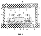
- Fig. 8 illustrates the main chamber (36) of the flat-panel CRT display.
- the chamber has an inlet/outlet port (42) through which gas can enter and leave the chamber.
- a selected gas such as hydrogen, helium, neon, argon, krypton, xenon, nitrogen, oxygen, fluorine, chlorine, bromine, iodine, chloromethane, dichloromethane, trichloromethane (chloroform), carbon tetrachloride, carbon tetrafluoride, fluoromethane, difluoromethane, an alkane varying from methane through octane, an alkene varying from ethene (ethylene) through octene, an alkyne varying from ethyne (acetylene) through octyne, an alkanol varying from methanol through hexanol, a ketone varying from acetone_through hexanone, an aldehyde varying from methanal through hexanal, formic acid, acetic acid, propionic acid, water, hydrogen peroxide, hydrazine,
- the flat-panel display is then operated, causing electron-emissive cones 10 of the field emitter to emit electrons that move towards the light-emitting device.
- part of the selected gas comes largely into contact with contaminant 12.
- the act of operating each cone 10 typically causes part of the selected gas to interact with contaminant 12 in such a way that contaminant 12 is converted to gaseous products 14. The interaction involves chemical reaction.
- Electron-emissive cone 10 in Fig. 1 can also be heated. Depending on the selected gas introduced into the main chamber, part or all of contaminant 12 may burn, thereby converting that contaminant material 12 to gaseous products 14. In this case, some residue (not shown) may be left on cone 10. Certain species, particularly certain oxide species, of contaminant 12 may volatize upon being heated.
- the main chamber is then re-evacuated through the inlet/outlet port to remove gaseous products 14 from the chamber.
- the chamber is typically pumped down to a pressure of 10 -7 torr or lower.
- Fig. 1c illustrates resulting cleaned electron-emissive cone 10, gaseous products 14 having been removed from the vicinity of cone 10.
- the port is permanently closed to seal the chamber and make it air tight. The process of Fig. 1 is complete.
- FIG. 1 An alternative technique, represented by Fig. 1 in certain applications, is to subject the structure of Fig. 1a to an oxygen plasma that converts contaminant material 12 to gaseous products 14. If substantially none of the material of electron-emissive cone 10 is oxidized during the oxygen plasma step, Fig. 1b represents the structure at the end of the plasma step. Should part of the material of cone 10 oxidize during the plasma step, this alternative technique is generally represented by the steps shown in Figs. 3a - 3d or 6a - 6d, discussed below. In that case, an oxide etch, likewise discussed below, is performed to remove the oxide from the conical surface of cone 10.
- FIG. 2 Another technique for cleaning metallic electron-emissive elements 10 of a field emitter according to the invention is illustrated in Figs. 2a - 2c (collectively "Fig. 2").
- the starting point for the process of Fig. 2 is the structure of Fig. 1a, repeated here as Fig. 2a, in which contaminant material 12 overlies the conical outside surface of electron-emissive element 10.
- contaminant material 12 overlies the conical outside surface of electron-emissive element 10.
- at least part of contaminant 12 is known, or expected to be, of such a nature that it is difficult to directly remove that contaminant in a rapid or/and efficient manner without damaging cone 10 or removing an excessive amount of cone 10.
- the first step in the process of Fig. 2 is to convert contaminant material 12 into further contaminant material 16 that can be removed rapidly, efficiently, and selectively from electron-emissive cone 10 without damaging cone 10. See Fig. 2b.
- This conversion step can be implemented by causing selected additional material to react with original contaminant 12 to form further contaminant 16.
- the additional material can be in gas-phase and/or liquid-phase form.
- the conversion of original contaminant 12 to further contaminant 16 can be performed by subjecting contaminant 12 to suitable actinic radiation that causes contaminant 12 to change chemical composition.
- UV Ultraviolet
- further contaminant 16 can be created from original contaminant 12 by applying actinic radiation to additional material and causing contaminant 12 to react with the additional material.
- the two actinic radiation steps can be performed simultaneously or one after the other.
- Fig. 2c which repeats Fig. 1c, depicts the cleaned version of cone 10.
- contaminant 16 can be dissolved in liquid etchant which does not significantly attack electron-emissive cone 10. Part of contaminant 16 can be converted into particles that become suspended in the liquid etchant. A plasma, which likewise does not significantly attack cone 10, can be employed to remove contaminant 16. Depending on its constituency, contaminant 16 can also be removed by utilizing suitable actinic radiation that converts contaminant 16 into gaseous products that move away from cone 10. Two or more of these techniques can be employed to remove contaminant 16 from cone 10.
- Figs. 3a - 3d depict a third technique for cleaning metallic electron-emissive elements 10 of a field emitter in accordance with the claimed method.
- the process of Fig. 3 likewise begins with the structure of Fig. 1a, now repeated as Fig. 3a.
- Surface coatings 18 are formed along the conical surfaces of electron-emissive elements 10 as overlying contaminant material 12 is converted into gaseous products 14 that move away from cone 10.
- Fig. 3b depicts the structure at this point.
- Surface coating 18 for electron-emissive cone 10 in Fig. 3b can be created in various ways. Typically, part of the material along the conical surface of cone 10 is reacted with additional material to form coating 18. The reaction can be enhanced by simultaneously subjecting cone 10 to actinic radiation, again typically UV light. The reaction may also be enhanced by heating cone 10 or subjecting it to infrared radiation.
- Surface coating 18 is typically created by oxidizing a small thickness of the emitter material along the conical surface of cone 10.
- cone 10 and contaminant material 12 can be subjected to an oxygen plasma that creates coating 18 and simultaneously converts at least part of contaminant 12 into gaseous products 14.
- cone 10 and contaminant 12 can be subjected simultaneously to diatomic (gas-phase) oxygen and actinic radiation, typically UV light, that causes part of the diatomic oxygen to form monatomic oxygen and ozone.
- diatomic oxygen is not highly reactive at low temperature
- monatomic oxygen and ozone are both highly reactive at low temperature and react with the emitter material along the conical surface of cone 10 to form coating 18.
- the UV/oxygen treatment normally done at no more than 50°C, typically causes at least part of contaminant 12 to be converted into gaseous products 14.
- gaseous products 14 that move away from electron-emissive cone 10 as surface coating 18 is formed.
- gaseous products 14 can be formed as an attendant effect of the reaction involved in creating coating 18.
- actinic radiation such as UV light
- actinic radiation can be separately utilized to convert part or all of contaminant 12 to the gas phase. Rapid heating (i.e., rapid thermal processing) can be used to vaporize contaminant 12 if it is volatile at relatively high temperature.
- Surface coating 18 may, or may not, impair the emission performance of electron-emissive cone 10. If the emission performance is impaired, coating 18 is at least partially removed.
- Fig. 3c illustrates a situation in which part of coating 18 is removed. The remaining portion of coating 18 is indicated as item 18A. Coating 18 can be fully removed as shown in Fig. 3d, which repeats Fig. 1c.
- the partial or total removal of surface coating 18 can be accomplished in various ways.
- coating 18 is formed as an oxide of the emitter material, part or all of coating 18 can be removed with a suitable plasma, typically a hydrogen plasma.
- coating 18 can be partially or totally dissolved in a liquid chemical etchant. This typically entails immersing cone 10 in the liquid etchant.
- a typical liquid etchant for partially or totally removing coating 18 is an aqueous solution of tris-(hydromethyl)amino methane at approximately 60°C.
- cone 10 and coating 18 can undergo an operation in which the additional material, such as oxygen, utilized to form coating 18 is removed from coating 18, thereby converting coating 18 back into the emitter material of cone 10. This conversion is simply a reduction when coating 18 is an oxide of the emitter material.
- Fig. 3d also represents the final structure of cone 10 for this alternative.
- FIG. 4a A fourth technique for cleaning metallic electron-emissive elements 10 of a field emitter in accordance with the claimed method is depicted in Figs. 4a - 4d (collectively "Fig. 4").
- Fig. 1a The structure of Fig. 1a, repeated here as Fig. 4a, is the starting point for the process of Fig. 4.
- surface coating 18 is formed along the conical surface of electron-emissive element 10.
- coating 18 can be formed in any of the ways described above for the process of Fig. 3.
- contaminant 12 in the process of Fig. 4 continues to overlie cone 10 as surface coating 18 is formed below contaminant 12. See Fig. 4b.
- part or all of contaminant 12 may be converted to a different chemical form, similar to further contaminate 16 in the process of Fig. 2, during the formation of coating 18.
- Contaminant material 12 (including any portion of changed chemical form) is subsequently removed.
- the removal of contaminant 12 is typically accomplished by removing at least part of surface coating 18. Contaminant 12 is then lifted off.
- the partial or total removal of surface coating 18 can be performed in any of the ways described above for the process of Fig. 3.
- a plasma such as a hydrogen plasma
- various mechanisms may come into action for transporting contaminant material 12 away from the vicinity of cone 10.
- contaminant 12 can be swept away in the flow of gas and plasma components through the plasma chamber.
- contaminant 12 can become suspended in the plasma due to the accumulation of electrostatic charge.
- contaminant material 12 When coating 18 is partially or totally removed with a liquid chemical etchant, contaminant material 12 normally dissolves and/or becomes suspended in the etchant. Stirring of the etchant may be performed to move particles of contaminant 12 away from cone 10 and prevent those particles from redepositing on cone 10. This can, for instance, be implemented by ultrasonic agitation of the etchant. Filtration can also be employed to inhibit redeposition of contaminant 12 on cone 10.
- Fig. 4c illustrates the situation in which the lift off of contaminant material 12 is achieved by removing part of surface coating 18.
- Item 18A is the remainder of surface coating 18.
- the presence of reduced-thickness surface coating 18A normally does not significantly degrade the emission performance of cone 10, and may indeed enhance the emission performance.
- Fig. 4d illustrates the condition in which the removal of coating 18 is continued until it is totally removed.
- Figs. 1 - 4 can be combined in various ways.
- Fig. 5 illustrates how a combination of the techniques of Figs. 1 and 2 is employed for cleaning metallic electron-emissive cones 10 of a field emitter in accordance with the invention.
- the starting point is again the structure of Fig. 1a, now repeated as Fig. 5a.
- Part of contaminant material 12 is converted into gaseous products 14 that move away from cone 10 as indicated in Fig. 5b.
- the remainder of contaminant 12 is converted into further contaminant material 16 which overlies cone 10 but is more readily removable from cone 10 than original contaminant 12.
- the conversion of contaminant 12 into gaseous products 14 and further contaminant 16 can be done in one operation or in separate operations.
- Fig. 6 illustrates how the techniques of Figs. 3 and 4 are combined in accordance with the claimed method to clean metallic electron-emissive cones 10 of a field emitter.
- the process of Fig. 6 begins with the structure of Fig. 1a, here repeated as Fig. 6a.
- Surface coating 18 is formed along the conical surface of cone 10 below portions of contaminant material 12 as shown in Fig. 6b. Similar to the process Fig. 4, part of all of these portions of contaminant 12 may be converted to different chemical form during the creation of coating 18. The remainder of contaminant 12 is converted into gaseous products 14 that move away from cone 10.
- the formation of coating 18 and the partial conversion of part of contaminant 12 into gaseous products 14 can be done in one operation or in separate operations.
- Fig. 6c illustrates the resultant structure when part of coating 18 is removed, item 18A again indicating the remainder of coating 18.
- Fig. 6d illustrates the structure when coating 18 is fully removed.
- Figs. 7a - 7c, 7d1, 7e1, 7d2 - 7g2, 7d3 - 7f3, and 7d4 - 7f4 illustrate a general technique, including a number of processing branches, for treating metallic electron-emissive elements 10 of a field emitter in accordance with the invention so as to keep electron-emissive elements 10 clean.
- the process of Fig. 7 begins with elements 10 in a largely clean condition. See Fig. 7a.
- the structure of Fig. 7a represents the situation in which electron-emissive cone 10 has just been cleaned, for example, according to any of the techniques of Figs. 1 - 6 or in which the fabrication of cone 10 has recently been completed and cone 10 is under vacuum and can be accessed through an inlet/outlet port.
- a surface coating 20 is formed along the conical outside surface of electron-emissive element 10 as depicted in Fig. 7b.
- Surface coating 20 can be created according to any of the procedures used to form surface coating 18 in the process of Fig. 3.
- coating 20 can be formed by reacting a small thickness of the material of cone 10 with additional material, typically a gas such as oxygen.
- Contaminant material 12 subsequently accumulates over surface coating 20 as shown in Fig. 7c.
- Various procedures can be employed to remove contaminant 12.
- Figs. 7d1, 7e1, 7d2 - 7g2, 7d3 - 7f3, and 7d4 - 7f4 present four such procedures, each group of figures whose figure numbers end with the same numerical value representing a different one of the procedures.
- Figs. 7d1 and 7e1 part or all of surface coating 20 can be removed to lift off contaminant material 12.
- Fig. 7d1 illustrates the situation in which part of coating 20 is removed.
- Item 20A is the remainder of coating 20.
- Fig. 7e1 illustrates the situation in which all of coating 20 is removed.
- contaminant 12 is converted into gaseous products 14 that move away from cone 10. See Fig. 7d2.
- Coating 20 may improve the emission performance of cone 10 or, at the minimum, not significantly degrade the emission performance. If so, coating 20 can be left in place as represented in Fig. 7e2. Alternatively, part of coating 20 can be removed as shown in Fig. 7f2 in which item 20A is again the remainder of coating 20. Finally, Fig. 7g2 illustrates the case in which coating 20 is totally removed.
- contaminant material 12 is converted into further contaminant material 16 as shown in Fig. 7d3.
- Further contaminant 16 may be more easily removed from coating 20 than original contaminant 12. If so, further contaminant 16 can be separately removed without significantly affecting coating 20. Alternatively, part or all of coating 20 can be removed to lift off contaminant 16.
- Figs. 7e3 and 7f3 respectively represent the cases in which coating 20 is partially and fully removed.
- Figs. 7d4 - 7f4 illustrate how the procedure of Figs. 7d3 - 7f3 is combined with that of Figs. 7d2 - 7g2. Part of contaminant 12 is converted into further contaminant 16 while the remainder of original contaminant 12 is converted into gaseous products 14 that move away from cone 10. See Fig. 7d4. Further contaminant 16, which may be more easily removed from surface coating 20 than original contaminant 12, is subsequently removed. Fig. 7e4 illustrates the situation in which at least part of coating 20 is removed to lift off further contaminant 16. The removal of all of coating 20 is represented by the structure of Fig. 7f4.
- Fig. 8 illustrates an example of a flat-panel CRT display having a field emitter 30 which employs electron-emissive cones 10 that are cleaned according to the invention.
- the components of the flat-panel display include a light-emitting device 32 and an annular outer wall 34.
- Field emitter 30 and light emitting device 32 are joined together through outer wall 34, typically glass, to form a chamber 36.
- Item 38 in Fig. 8 indicates sealing material, typically glass frit, by which outer wall 34 is joined to field emitter 30.
- Item 40 similarly indicates sealing material, again typically glass frit, by which wall 34 is joined to light-emitting device 32.
- the flat-panel display has an inlet/outlet port 42 through which gas can be introduced into, and removed from, chamber 36.
- Inlet/outlet port 42 is shown as extending through a peripheral portion of field emitter 30 in Fig. 8.
- Fig. 8 depicts port 42 in its open condition.
- the pressure in chamber 36 is reduced to 10 -7 torr or less, and port 42 is permanently closed to make chamber 36 air tight.
- Field emitter 30 is created from a thin flat electrically insulating baseplate 50 typically consisting of glass.
- a lower electrically non-insulating emitter region lies on top of baseplate 50.
- the lower emitter region typically consists of (a) a group of laterally separated generally parallel emitter electrodes 52 situated on baseplate 50 and (b) an electrically resistive layer 54.
- Emitter electrodes 52 typically consist of metal such as aluminum or nickel.
- Resistive layer 54 typically consists of cermet and/or a silicon-carbon-nitrogen compound.
- a dielectric layer 56 typically consisting of silicon oxide or silicon nitride, is situated on resistive layer 54 and may contact baseplate 50 depending on the shape of layer 54.
- a group of laterally separated generally parallel control electrodes 58 extend across dielectric layer 56 generally perpendicular to emitter electrodes 50.
- Two control electrodes 58 are depicted in Fig. 8.
- Each control electrode 58 consists of (a) a main control portion 60 that extends the length of that control electrode 58 and (b) one or more thinner adjoining gate portions 62.
- Main control portions 60 and gate portions 62 both typically consist of chromium.
- a multiplicity of composite openings extend through gate portions 62 and dielectric layer 56 down to resistive layer 54 of the lower non-insulating region.
- Each composite opening consists of (a) a gate opening 64 extending through one of gate portions 62 and (b) a dielectric opening 66 extending through dielectric layer 56.
- Each composite opening 64/66 contains one electron-emissive cone 10. Accordingly, cones 10 are situated along the inside of chamber 36. Cones 10 are arranged in a two-dimensional array of laterally separated sets of multiple cones 10.
- Field emitter 30 also contains an electron focusing system 68 arranged generally in a waffle-like pattern.
- Focusing system 68 consists of a base focusing structure 70 and an adjoining focus coating 72.
- Base focusing structure 70 is typically formed with electrically resistive material or electrically insulating material.
- Focus coating 72 is formed with electrically non-insulating material, typically metal.
- Focusing system 68 controls the trajectories of electrons emitted by electron-emissive cones 10 so that they strike intended portions of light-emitting device 32.
- the cleaning techniques of the invention overcome contamination of cones 10 that occurs during the formation of focusing system 68.
- Light-emitting device 32 is created from a thin flat transparent electrically insulating faceplate 80 typically glass, located across from baseplate 50.
- Light-emitting phosphor regions 82 are situated on the interior surface of faceplate 80 directly across from corresponding sets of electron-emissive elements 10.
- a thin light-reflective layer 84 typically aluminum, overlies phosphor regions 82 along the interior surface of faceplate 80. Electrons emitted by electron-emissive elements 10 pass through light-reflective layer 84 and cause phosphor regions 82 to emit light that produces an image visible on the exterior surface of faceplate 80.
- the flat-panel CRT display typically includes other components not shown in Fig. 8.
- a getter is provided to remove contaminant gases that enter chamber 36 after final display sealing, typically as a result of operating the display or by penetration of the seal.
- a black matrix situated along the interior surface of faceplate 80 typically surrounds each phosphor region 82 to laterally separate it from other phosphor regions 82. Spacer walls are utilized to maintain a relatively constant spacing between baseplate 50 and faceplate 80.
- Light-reflective layer 84 serves as an anode for the field-emission cathode.
- the anode is maintained at high positive potential relative to the electrodes 52 and 58.
- the so-selected gate portion 62 extracts electrons from electron-emissive elements 10 at the intersection of the two selected electrodes and controls the magnitude of the resulting electron current. Desired levels of electron emission typically occur when the applied gate-to-cathode parallel-plate electric field reaches 20 - 100 volts/mm or less at a current density of 0.1 mA/cm 2 as measured at phosphor-coated faceplate 80 when phosphor regions 82 are high-voltage phosphors. Upon being hit by the extracted electrons, phosphor regions 82 emit light.
- electron-emissive elements 10 can have shapes other than cones.
- One example is filaments.
- Another example is cones on pedestals.
- Electron-emissive elements 10 can be utilized in electron-emitting devices that operate according to mechanisms such as thermionic emission and photoemission. Electron-emitting devices that contain electron-emissive elements 10 cleaned according to the invention can be employed in flat-panel products other than flat-panel CRT displays. Examples include products utilized in electron spectroscopy, in generating X rays or microwaves from electron beams, and in evaporating materials by electron-beam heating. Various modifications and applications may thus be made by those skilled in the art without departing from the scope of the invention as defined in the appended claims.
Landscapes
- Engineering & Computer Science (AREA)
- Manufacturing & Machinery (AREA)
- Cold Cathode And The Manufacture (AREA)
- Manufacture Of Electron Tubes, Discharge Lamp Vessels, Lead-In Wires, And The Like (AREA)
- Cleaning In General (AREA)
Description
Claims (16)
- A method for removing contaminant material (12) overlying electron-emissive elements (10) of an electron-emitting device, comprising:converting the contaminant material into another material (14); andremoving the converted contaminant material (14) from the electron-emissive elements (10).
- A method as in Claim 1, wherein:converting the contaminant material entails introducing selected gas-phase material into a chamber of a product containing the electron-emitting device such that the selected gas-phase material comes substantially into contact with the contaminant material to form gaseous products that move away from the electron-emissive elements; and whereinremoving the converted contaminant material entails largely removing the gaseous products from the chamber.
- A method as in Claim 2 further including, before the converting step, the step of largely evacuating the chamber.
- A method as in any of Claims 2-3 wherein the selected gas-phase material comprises at least one of hydrogen, helium, neon, argon, krypton, xenon, nitrogen, oxygen, fluorine, chlorine, bromine, iodine, chloromethane, dichloromethane, trichloromethane, carbon tetrachloride, carbon tetrafluoride, fluoromethane, difluoromethane, an alkane varying from methane through octane, an alkene varying from ethene through octene, an alkyne varying from ethyne through octyne, an alkanol varying from methanol through hexanol, a ketone varying from acetone through hexanone, an aldehyde varying from methanal through hexanal, formic acid, acetic acid, propionic acid, water, hydrogen peroxide, hydrazine, nitrous oxide, nitric oxide, nitrogen dioxide, carbon monoxide, carbon dioxide, ammonia, phosphine, arsine, stibine, hydrogen fluoride, hydrogen chloride, hydrogen bromide, hydrogen iodide, boron fluoride, diborane, nitrogen trifluoride, hydrogen sulfide, hydrogen selenide, hydrogen telluride, and sulfur dioxide.
- A method as in any of Claims 2-4 wherein the converting step includes operating the electron-emissive elements.
- A method as in Claim 1, wherein converting the contaminant material comprises converting the contaminant material into further material overlying the electron-emissive elements.
- A method as in Claim 6 wherein the converting step comprises reacting at least part of the contaminant material with additional material to produce the further material.
- A method as in Claim 6 wherein the converting step comprises subjecting the contaminant material to actinic radiation:
- A method as in Claim 6 wherein the converting step further includes reacting at least part of the contaminant material with additional material to produce at least part of the further material.
- A method as in any of Claims 6-9 wherein the removing step comprises dissolving the further material in a liquid and/or causing particles of the further material to become suspended in the liquid.
- A method as in any of Claims 6-9 wherein the removing step comprises subjecting the further material to a plasma.
- A method as in Claim 6 wherein the converting and removing steps entail converting the further contaminant material overlying the electron-emissive elements into gaseous products that move away from the electron-emissive elements.
- A method as in Claim 12 wherein the converting and removing steps further entail operating the electron-emissive elements.
- A method as in Claim 12 or 13 wherein the removing step includes removing the gaseous products from a chamber of a product containing the electron-emitting device.
- A method as in any of Claims 1-14 wherein the electron-emissive elements are largely metallic.
- A method as in Claims 1-14 wherein the electron-emitting device comprises:a group of laterally separated emitter electrodes;a dielectric layer overlying the emitter electrode; anda group of control electrodes overlying the dielectric layer and crossing over the emitter electrodes, the electron-emissive elements situated above the emitter electrodes in composite openings extending through the control electrodes and the dielectric layer.
Applications Claiming Priority (3)
| Application Number | Priority Date | Filing Date | Title |
|---|---|---|---|
| US940873 | 1997-09-30 | ||
| US08/940,873 US6004180A (en) | 1997-09-30 | 1997-09-30 | Cleaning of electron-emissive elements |
| PCT/US1998/018509 WO1999017323A2 (en) | 1997-09-30 | 1998-09-22 | Cleaning of electron-emissive elements |
Publications (3)
| Publication Number | Publication Date |
|---|---|
| EP1021818A2 EP1021818A2 (en) | 2000-07-26 |
| EP1021818A4 EP1021818A4 (en) | 2001-04-04 |
| EP1021818B1 true EP1021818B1 (en) | 2005-11-30 |
Family
ID=25475565
Family Applications (1)
| Application Number | Title | Priority Date | Filing Date |
|---|---|---|---|
| EP98950613A Expired - Lifetime EP1021818B1 (en) | 1997-09-30 | 1998-09-22 | Cleaning of electron-emissive elements |
Country Status (6)
| Country | Link |
|---|---|
| US (1) | US6004180A (en) |
| EP (1) | EP1021818B1 (en) |
| JP (1) | JP4323092B2 (en) |
| KR (1) | KR100387053B1 (en) |
| DE (1) | DE69832633T2 (en) |
| WO (1) | WO1999017323A2 (en) |
Families Citing this family (24)
| Publication number | Priority date | Publication date | Assignee | Title |
|---|---|---|---|---|
| US6149483A (en) * | 1998-07-30 | 2000-11-21 | Candescent Technologies Corporation | Cleaning of components of flat panel display |
| US6624592B1 (en) * | 1998-08-31 | 2003-09-23 | Candescent Intellectual Property Services, Inc | Procedures and apparatus for turning-on and turning-off elements within a field emission display device |
| JP2000133736A (en) * | 1998-10-26 | 2000-05-12 | Furukawa Electric Co Ltd:The | Hermetic sealing method and hermetic sealing device for semiconductor laser device |
| FR2805663A1 (en) * | 2000-02-25 | 2001-08-31 | Pixtech Sa | Field effect flat display screen plasma cleaning technique having plasma internal space between base/screen surface outside electrodes generated and following cleaning vacuum/sealing applied. |
| US6738336B2 (en) * | 2001-05-16 | 2004-05-18 | Hewlett-Packard Development Company, L.P. | Data storage device |
| US6873097B2 (en) * | 2001-06-28 | 2005-03-29 | Candescent Technologies Corporation | Cleaning of cathode-ray tube display |
| DE10209493B4 (en) * | 2002-03-07 | 2007-03-22 | Carl Zeiss Smt Ag | Method for avoiding contamination on optical elements, device for controlling contamination on optical elements and EUV lithography device |
| KR100438590B1 (en) * | 2002-08-16 | 2004-07-02 | 엘지전자 주식회사 | Aging apparatus for flat type field emission display and aging method thereof |
| JP2004288547A (en) * | 2003-03-24 | 2004-10-14 | Matsushita Electric Ind Co Ltd | Field emission type electron source, manufacturing method thereof and image display device |
| US7081992B2 (en) * | 2004-01-16 | 2006-07-25 | Euv Llc | Condenser optic with sacrificial reflective surface |
| US8053872B1 (en) | 2007-06-25 | 2011-11-08 | Rf Micro Devices, Inc. | Integrated shield for a no-lead semiconductor device package |
| US8062930B1 (en) | 2005-08-08 | 2011-11-22 | Rf Micro Devices, Inc. | Sub-module conformal electromagnetic interference shield |
| US20090000815A1 (en) * | 2007-06-27 | 2009-01-01 | Rf Micro Devices, Inc. | Conformal shielding employing segment buildup |
| US8959762B2 (en) | 2005-08-08 | 2015-02-24 | Rf Micro Devices, Inc. | Method of manufacturing an electronic module |
| US20080315101A1 (en) * | 2007-06-20 | 2008-12-25 | Chien-Min Sung | Diamond-like carbon infrared detector and associated methods |
| US9137934B2 (en) | 2010-08-18 | 2015-09-15 | Rf Micro Devices, Inc. | Compartmentalized shielding of selected components |
| US8835226B2 (en) | 2011-02-25 | 2014-09-16 | Rf Micro Devices, Inc. | Connection using conductive vias |
| US9627230B2 (en) | 2011-02-28 | 2017-04-18 | Qorvo Us, Inc. | Methods of forming a microshield on standard QFN package |
| US9807890B2 (en) | 2013-05-31 | 2017-10-31 | Qorvo Us, Inc. | Electronic modules having grounded electromagnetic shields |
| US11127689B2 (en) | 2018-06-01 | 2021-09-21 | Qorvo Us, Inc. | Segmented shielding using wirebonds |
| US11219144B2 (en) | 2018-06-28 | 2022-01-04 | Qorvo Us, Inc. | Electromagnetic shields for sub-modules |
| US11114363B2 (en) | 2018-12-20 | 2021-09-07 | Qorvo Us, Inc. | Electronic package arrangements and related methods |
| US11515282B2 (en) | 2019-05-21 | 2022-11-29 | Qorvo Us, Inc. | Electromagnetic shields with bonding wires for sub-modules |
| US12340969B2 (en) | 2022-03-18 | 2025-06-24 | Kla Corporation | Electron gun and electron microscope |
Family Cites Families (5)
| Publication number | Priority date | Publication date | Assignee | Title |
|---|---|---|---|---|
| DE3639657A1 (en) * | 1986-11-20 | 1988-06-01 | Philips Patentverwaltung | METHOD FOR CLEANING METAL COMPONENTS FOR CATHODE RAY TUBES |
| FR2719155B1 (en) * | 1994-04-25 | 1996-05-15 | Commissariat Energie Atomique | Method for producing microtip electron sources and microtip electron source obtained by this method. |
| FR2719156B1 (en) * | 1994-04-25 | 1996-05-24 | Commissariat Energie Atomique | Source of microtip electrons, microtips having two parts. |
| US5470266A (en) * | 1994-07-06 | 1995-11-28 | Itt Corporation | Low temperature process and apparatus for cleaning photo-cathodes |
| US5462468A (en) * | 1994-12-16 | 1995-10-31 | Philips Electronics North America Corporation | CRT electron gun cleaning using carbon dioxide snow |
-
1997
- 1997-09-30 US US08/940,873 patent/US6004180A/en not_active Expired - Lifetime
-
1998
- 1998-09-22 KR KR10-2000-7003359A patent/KR100387053B1/en not_active Expired - Fee Related
- 1998-09-22 JP JP2000514296A patent/JP4323092B2/en not_active Expired - Fee Related
- 1998-09-22 DE DE69832633T patent/DE69832633T2/en not_active Expired - Lifetime
- 1998-09-22 EP EP98950613A patent/EP1021818B1/en not_active Expired - Lifetime
- 1998-09-22 WO PCT/US1998/018509 patent/WO1999017323A2/en not_active Ceased
Also Published As
| Publication number | Publication date |
|---|---|
| WO1999017323A2 (en) | 1999-04-08 |
| KR100387053B1 (en) | 2003-06-12 |
| DE69832633T2 (en) | 2006-08-17 |
| DE69832633D1 (en) | 2006-01-05 |
| US6004180A (en) | 1999-12-21 |
| WO1999017323A3 (en) | 1999-09-02 |
| EP1021818A4 (en) | 2001-04-04 |
| KR20010030782A (en) | 2001-04-16 |
| JP2001518682A (en) | 2001-10-16 |
| HK1031154A1 (en) | 2001-06-01 |
| JP4323092B2 (en) | 2009-09-02 |
| EP1021818A2 (en) | 2000-07-26 |
Similar Documents
| Publication | Publication Date | Title |
|---|---|---|
| US6004180A (en) | Cleaning of electron-emissive elements | |
| US5666025A (en) | Flat-panel display containing structure for enhancing electron emission from carbon-containing cathode | |
| JP5301168B2 (en) | Cold field emitter | |
| US6780075B2 (en) | Method of fabricating nano-tube, method of manufacturing field-emission type cold cathode, and method of manufacturing display device | |
| KR100245910B1 (en) | Manufacturing method of pseudo diamond thin film, analogous diamond thin film, field emission array and field emitter cathode | |
| US20040043219A1 (en) | Pattern forming method for carbon nanotube, and field emission cold cathode and method of manufacturing the cold cathode | |
| KR20010056153A (en) | Field emission display device and its fabrication method | |
| EP0501785A2 (en) | Electron emitting structure and manufacturing method | |
| WO1997033297A1 (en) | Electrochemical removal of material, particularly excess emitter material in electron-emitting device | |
| US6953701B2 (en) | Process for sharpening tapered silicon structures | |
| Yavas et al. | Maskless fabrication of field-emitter array by focused ion and electron beam | |
| US6469425B1 (en) | Electron emission film and field emission cold cathode device | |
| US7588475B2 (en) | Field-emission electron source, method of manufacturing the same, and image display apparatus | |
| Rakhshandehroo et al. | High current density Si field emission devices with plasma passivation and HfC coating | |
| KR19990038696A (en) | Method of manufacturing cathode tips of field emission devices | |
| HK1031154B (en) | Cleaning of electron-emissive elements | |
| US6116974A (en) | Spacers, display devices containing the same, and methods for making and using the same | |
| US6890446B2 (en) | Uniform emitter array for display devices, etch mask for the same, and methods for making the same | |
| US6573642B1 (en) | Field emission device and method for the conditioning thereof | |
| Mao et al. | Electron field emission from a patterned diamondlike carbon flat cathode | |
| JPH08255555A (en) | Needle electrode and manufacturing method thereof | |
| KR100246254B1 (en) | Manufacturing method of field emission device having silicide as emitter and gate | |
| KR100278502B1 (en) | Manufacturing method of volcanic metal FEA with double gate | |
| KR100186253B1 (en) | Method of manufacturing silicon fea by locos | |
| KR100452693B1 (en) | Method Of Fabricating Field Emission Device |
Legal Events
| Date | Code | Title | Description |
|---|---|---|---|
| PUAI | Public reference made under article 153(3) epc to a published international application that has entered the european phase |
Free format text: ORIGINAL CODE: 0009012 |
|
| 17P | Request for examination filed |
Effective date: 20000428 |
|
| AK | Designated contracting states |
Kind code of ref document: A2 Designated state(s): DE FR GB IE NL |
|
| A4 | Supplementary search report drawn up and despatched |
Effective date: 20010219 |
|
| AK | Designated contracting states |
Kind code of ref document: A4 Designated state(s): DE FR GB IE NL |
|
| RIC1 | Information provided on ipc code assigned before grant |
Free format text: 7H 01J 7/00 A, 7H 01J 9/02 B |
|
| 17Q | First examination report despatched |
Effective date: 20031124 |
|
| GRAP | Despatch of communication of intention to grant a patent |
Free format text: ORIGINAL CODE: EPIDOSNIGR1 |
|
| RAP1 | Party data changed (applicant data changed or rights of an application transferred) |
Owner name: CANON INC. |
|
| GRAS | Grant fee paid |
Free format text: ORIGINAL CODE: EPIDOSNIGR3 |
|
| RAP1 | Party data changed (applicant data changed or rights of an application transferred) |
Owner name: CANON INC.(CANON KABUSHIKI KAISHA) |
|
| GRAA | (expected) grant |
Free format text: ORIGINAL CODE: 0009210 |
|
| AK | Designated contracting states |
Kind code of ref document: B1 Designated state(s): DE FR GB IE NL |
|
| PG25 | Lapsed in a contracting state [announced via postgrant information from national office to epo] |
Ref country code: NL Free format text: LAPSE BECAUSE OF FAILURE TO SUBMIT A TRANSLATION OF THE DESCRIPTION OR TO PAY THE FEE WITHIN THE PRESCRIBED TIME-LIMIT Effective date: 20051130 |
|
| REG | Reference to a national code |
Ref country code: GB Ref legal event code: FG4D |
|
| REG | Reference to a national code |
Ref country code: IE Ref legal event code: FG4D |
|
| REF | Corresponds to: |
Ref document number: 69832633 Country of ref document: DE Date of ref document: 20060105 Kind code of ref document: P |
|
| NLV1 | Nl: lapsed or annulled due to failure to fulfill the requirements of art. 29p and 29m of the patents act | ||
| ET | Fr: translation filed | ||
| PG25 | Lapsed in a contracting state [announced via postgrant information from national office to epo] |
Ref country code: IE Free format text: LAPSE BECAUSE OF NON-PAYMENT OF DUE FEES Effective date: 20060922 |
|
| PLBE | No opposition filed within time limit |
Free format text: ORIGINAL CODE: 0009261 |
|
| STAA | Information on the status of an ep patent application or granted ep patent |
Free format text: STATUS: NO OPPOSITION FILED WITHIN TIME LIMIT |
|
| REG | Reference to a national code |
Ref country code: HK Ref legal event code: GR Ref document number: 1031154 Country of ref document: HK |
|
| 26N | No opposition filed |
Effective date: 20060831 |
|
| REG | Reference to a national code |
Ref country code: IE Ref legal event code: MM4A |
|
| PGFP | Annual fee paid to national office [announced via postgrant information from national office to epo] |
Ref country code: GB Payment date: 20120926 Year of fee payment: 15 |
|
| PGFP | Annual fee paid to national office [announced via postgrant information from national office to epo] |
Ref country code: DE Payment date: 20120930 Year of fee payment: 15 |
|
| PGFP | Annual fee paid to national office [announced via postgrant information from national office to epo] |
Ref country code: FR Payment date: 20121009 Year of fee payment: 15 |
|
| GBPC | Gb: european patent ceased through non-payment of renewal fee |
Effective date: 20130922 |
|
| REG | Reference to a national code |
Ref country code: DE Ref legal event code: R119 Ref document number: 69832633 Country of ref document: DE Effective date: 20140401 |
|
| REG | Reference to a national code |
Ref country code: FR Ref legal event code: ST Effective date: 20140530 |
|
| PG25 | Lapsed in a contracting state [announced via postgrant information from national office to epo] |
Ref country code: GB Free format text: LAPSE BECAUSE OF NON-PAYMENT OF DUE FEES Effective date: 20130922 |
|
| PG25 | Lapsed in a contracting state [announced via postgrant information from national office to epo] |
Ref country code: DE Free format text: LAPSE BECAUSE OF NON-PAYMENT OF DUE FEES Effective date: 20140401 Ref country code: FR Free format text: LAPSE BECAUSE OF NON-PAYMENT OF DUE FEES Effective date: 20130930 |