EP1018778B1 - Multi-layered patch antenna - Google Patents
Multi-layered patch antenna Download PDFInfo
- Publication number
- EP1018778B1 EP1018778B1 EP99124675A EP99124675A EP1018778B1 EP 1018778 B1 EP1018778 B1 EP 1018778B1 EP 99124675 A EP99124675 A EP 99124675A EP 99124675 A EP99124675 A EP 99124675A EP 1018778 B1 EP1018778 B1 EP 1018778B1
- Authority
- EP
- European Patent Office
- Prior art keywords
- plane
- patch
- dielectric layer
- feed member
- ground plane
- Prior art date
- Legal status (The legal status is an assumption and is not a legal conclusion. Google has not performed a legal analysis and makes no representation as to the accuracy of the status listed.)
- Expired - Lifetime
Links
Images

Classifications
-
- H—ELECTRICITY
- H01—ELECTRIC ELEMENTS
- H01Q—ANTENNAS, i.e. RADIO AERIALS
- H01Q3/00—Arrangements for changing or varying the orientation or the shape of the directional pattern of the waves radiated from an antenna or antenna system
- H01Q3/44—Arrangements for changing or varying the orientation or the shape of the directional pattern of the waves radiated from an antenna or antenna system varying the electric or magnetic characteristics of reflecting, refracting, or diffracting devices associated with the radiating element
- H01Q3/46—Active lenses or reflecting arrays
-
- H—ELECTRICITY
- H01—ELECTRIC ELEMENTS
- H01Q—ANTENNAS, i.e. RADIO AERIALS
- H01Q5/00—Arrangements for simultaneous operation of antennas on two or more different wavebands, e.g. dual-band or multi-band arrangements
- H01Q5/40—Imbricated or interleaved structures; Combined or electromagnetically coupled arrangements, e.g. comprising two or more non-connected fed radiating elements
- H01Q5/42—Imbricated or interleaved structures; Combined or electromagnetically coupled arrangements, e.g. comprising two or more non-connected fed radiating elements using two or more imbricated arrays
Definitions
- This invention relates to microstrip patch antennas and to arrays of such antennas and, more particularly, to a horn fed array for the generation of shaped or pencil beams.
- lens antennas are utilized to form shaped or pencil beams.
- an array of unit cells are formed on a single lens comprising a dielectric substrate with one or more conducting layers.
- the unit cells have stripline feed members which channel electromagnetic waves.
- the stripline feed members vary in length in order to provide appropriate phase differences required to generate the shaped/pencil beam.
- the electromagnetic radiation to be received or transmitted is typically provided directly to the feed member in the form of electrical power.
- the phase versus frequency characteristic of each unit cell is preferably linear in order to maintain the desired beam shape over a range of frequencies.
- DE 42 39 597 A1 discloses a dual-polarization planar antenna which includes: a first feeding substrate having a plurality of first radiation elements and a first feeding line; a first dielectric member; a first ground conductor having a plurality of slots; a second dielectric member; a second feeding substrate having a plurality of second radiation elements and a second feeding line; a third dielectric member; and a second ground conductor.
- the first feeding substrate, the first dielectric member, the first ground conductor, the second dielectric member, the second feeding substrate, the third dielectric member, and the second ground conductor are successively superposed in this order.
- the first feeding substrate, the first ground conductor, and the second feeding substrate are arranged so that the slots, the first radiation elements, and the second radiation elements are overlapped with one another at the same positions.
- the first and the second feeding substrates are arranged so that the first radiation elements are excited by the first feeding line in a first excitation direction, while the second radiation elements are excited by a second feeding line in a second excitation direction perpendicular to the first excitation direction.
- the present invention discloses a novel horn-fed, multi-layered, patch antenna which is capable of transmitting and receiving shaped or pencil beams without the need for direct electrical connections.
- the inventive antenna includes an array of unit cells. Each unit cell includes a transmitting patch, located on a first patch plane, and a feeding patch located on a second patch plane. Interposed between these patches are two ground planes each containing corresponding slots. The ground planes are separated by feed members which further correspond with the slots of both ground planes. These components are all configured within a dielectric substrate.
- the horn In operation, the horn emits electromagnetic waves which strike the second patch plane.
- the energy is coupled between the second and first patch planes via the slots and feed members.
- the feed members vary in length, or size, in order to provide appropriate phase differences required to generate the desired shaped or pencil beams. Since the feed members propagate in the transverse electromagnetic (TEM) mode, the phase versus frequency characteristic of each unit cell (patch-slot-feed-member-slot-patch) is linear. This has the advantage of maintaining the beam shape over a range of frequencies.
- TEM transverse electromagnetic
- the ability of the present invention to couple energy from the second patch plane to the first, via slots and feed members, eliminates the drawbacks of the previous art. Specifically, direct connections are no longer necessary to couple the feed patches to the transmitting patches or the feed members.
- the present invention thus has the further advantage of eliminating the need for layer piercing probes thereby simplifying the antenna manufacture. In addition, the elimination of the probe connection enhances temperature stability.
- inventive antenna over prior art is its flat structure, and light weight, making it ideal for packaging within a satellite application.
- the linear phase versus frequency characteristics make wide band applications possible and the antenna's center-fed structure helps to eliminate dispersion problems.
- a lens antenna structure 20 is preferred for use in a satellite 10 application as a result of its low profile and ease in which it can be configured to specialized geometries.
- Structure 20 is a horn-fed, multi-layered, printed circuit lens antenna particularly suited for shaped or pencil beams in the Ku and Ka bands.
- one embodiment of the lens antenna structure 20 is composed of a series of stacked layers.
- a first dielectric layer 22 is positioned adjacent to a first ground plane 24 which in turn is positioned adjacent to a second dielectric layer 26.
- the second dielectric layer 26 is positioned adjacent to a third dielectric layer 28 which in turn is adjacent to a second ground plane 30.
- the second ground plane 30 is positioned adjacent to a fourth dielectric layer 32.
- a feed member plane 34 Interposed between the second dielectric layer 26 and the third dielectric layer 28 is a feed member plane 34.
- positioned on a top surface 36 of the first dielectric layer 22 is a first patch plane 38, and positioned on a bottom surface 40 of the fourth dielectric layer 32 is a second patch plane 42.
- slots 50, 54 are arranged in the first and second ground planes 24, 30 respectively.
- Feed members 52 corresponding to slots 50, 54 are arranged in the third dielectric layer 28.
- the feed members 52 capacitively and electromagnetically couple the first and second patch planes 38, 42.
- a horn 44 remotely positioned below the second patch plane 42, emits electromagnetic energy in the direction of the antenna structure. This signal is received by the second patch plane 42, converted to TEM waves by the slots 50, 54 and feed members 52 in the intermediate ground planes 24, 30 and dielectric plane 28, and subsequently transmitted by the first patch plane 38.
- FIG 3 is a top view of a lens antenna structure 20 in accordance with one embodiment of the present invention.
- the lens antenna structure 20 comprises a plurality of unit cells 46.
- a unit cell 46 is shown in further detail in Figure 4.
- each unit cell 46 contains a portion of the layers and planes mentioned above.
- Each unit cell 46 comprises a first patch 48 from the first patch plane 38, a top slot 50 from the first ground plane 24, a feed member 52 from the feed member plane 34, a bottom slot 54 from the second ground plane 30, and a second patch 56 from the second patch plane 42.
- Each of the elements comprising the unit cell 46 are separated by a dielectric substrate.
- patch 48 is separated from slot 50 by the first dielectric layer 22; slot 50 is separated from feed member 52 by the second dielectric layer 26; feed member 52 is separated from slot 54 by the third dielectric layer 28; and slot 54 is separated from the second patch 56 by the fourth dielectric layer 32.
- the first patch 48 is substantially centered over the top slot 50, and the second patch 56 is centered beneath the bottom slot 54.
- the first patch 48 is off-centered from the second patch 56.
- the feed member 52 has a first end 58 positioned substantially perpendicular to the top slot 50, and a second end 60 positioned substantially perpendicular to the bottom slot 54.
- the feed member ends 58 and 60 extend to, and slightly beyond, the slots 50 and 54, respectively.
- the second patch 56 receives electromagnetic energy from the horn 44.
- Patch 56 radiates a frequency band centered at the second patch 56 resonance frequency.
- This radiation induces an electric field in the bottom slot 54 which extends transversely to the long dimension of the slot 54.
- This electric field creates a TEM wave which travels along feed member 52.
- This wave induces a second electric field in the top slot 50 which, in turn, excites first patch 48 at its resonating frequency.
- First patch 48 then transmits a frequency band centered about its resonating frequency.
- the feed member 52 can be configured in different shapes.
- the feed member 52 may be straight, so that the associated top slot 50 is parallel with the associated bottom slot 54, or the feed member 52 may be bent as shown in Figure 9.
- the preferred shape of the feed member 52 is a shape which positions the first end 58 orthogonal to the second end 60.
- Such a feed member shape permits variations of feed member lengths from one unit cell 46 to the next within the same array in a spacially efficient fashion.
- the orthogonal positioning of the first end 58 to the second end 60 simplifies manufacturing and reduces associated costs since the same patch plane pattern may be utilized for both the first patch plane 38 and the second patch plane 42.
- the same ground plane pattern may be utilized for the first and second ground planes 24, 30.
- “l” represents the distance from “s” to “s'" along the feed member 52.
- the feed member 52 propagates in the TEM mode, therefore the phase versus frequency characteristic of the unit cell 46 is linear (lines 106, 107, 108).
- the beam shape can be maintained over a range of frequencies.
- the transmitted bandwidth can be increased by using thicker substrate for the first and fourth dielectric layers 22, 32 and/or using stacked first patches 48.
- the stacked patches are approximately equal in size so as to resonate at approximately the same frequencies, but differ enough so as to broaden the bandwidth.
- the dielectric substrate utilized between stacked patches will also cause broadening of the transmitted frequency bandwidth.
- the dielectric constant is higher for the second and third dielectric layers 26, 28 than for the first and fourth dielectric layers 22, 32 in order to provide a sufficient electromagnetic coupling between the first patch 48 and the second patch 56.
- a high dielectric substrate in the feed region provides a large dynamic range for the phase.
- the lens antenna structure 20 In order to generate shaped or pencil beams, the lens antenna structure 20 must operate at appropriate phase differences. Phase differences are provided by varying the length of the feed member 52 from one unit cell 46 to the next. Figure 8 illustrates the phase shift versus feed member 52 length for a representative frequency (line 110).
- FIG. 9 shows another embodiment of a unit cell.
- a dual polarization application can be configured when utilizing a dual unit cell 62.
- Dual unit cell 62 is similar to unit cell 46 with an additional feed member 52 coupled with additional top and bottom slots 50, 54.
- the additional slots are spaced apart from, and positioned perpendicular to, the original slots. This positioning provides the preferred orthogonal coupling of electromagnetic radiation for dual polarization applications.
- the two polarizations are further isolated by a plurality of holes 64 plated with conductive metallic material connecting the respective ground planes in which slots 50 and 54 reside. To ensure proper isolation, the separation between the plurality of holes 64 is preferably less than 0.2 times the wavelength of the resonating frequency of the first and second patches 48 and 56.
- the present invention relates to an antenna structure being formed of a first patch plane, a first ground plane, a feed member plane, a second ground plane, and a second patch plane all spaced apart by layers of laminated dielectric substrate.
- a horn transmits energy upon the second patch plane.
- the energy is controlled in terms of phase and frequency, and is further electromagnetically coupled to the first patch plane which transmits in the form of shaped or pencil beams.
- the coupling between patch planes is accomplished by an array of slots located through the ground planes and an array of feed members interposed between the ground planes.
- the phase differences are established by utilization of feed members with different lengths.
Landscapes
- Physics & Mathematics (AREA)
- Electromagnetism (AREA)
- Waveguide Aerials (AREA)
- Aerials With Secondary Devices (AREA)
- Variable-Direction Aerials And Aerial Arrays (AREA)
Description
- This invention relates to microstrip patch antennas and to arrays of such antennas and, more particularly, to a horn fed array for the generation of shaped or pencil beams.
- In satellite applications, lens antennas are utilized to form shaped or pencil beams. Typically, an array of unit cells are formed on a single lens comprising a dielectric substrate with one or more conducting layers. The unit cells have stripline feed members which channel electromagnetic waves. The stripline feed members vary in length in order to provide appropriate phase differences required to generate the shaped/pencil beam. The electromagnetic radiation to be received or transmitted is typically provided directly to the feed member in the form of electrical power. The phase versus frequency characteristic of each unit cell is preferably linear in order to maintain the desired beam shape over a range of frequencies.
- A problem arises, however, in feeding the stripline feed members with electromagnetic radiation. Known devices use direct electrical connections between a radiating source and the feed members to permit transmission. As an example, a typical bootlace lens requires direct electrical connections between a feeding patch layer, the feed members, and a transmitting patch layer. Such connections, or probes, are difficult and expensive to manufacture. Furthermore, these probes produce temperature stability concerns. Accordingly, there exists a need for a simplified lens structure capable of transmitting and receiving shaped or pencil beams, which has simplified construction.
- DE 42 39 597 A1 discloses a dual-polarization planar antenna which includes: a first feeding substrate having a plurality of first radiation elements and a first feeding line; a first dielectric member; a first ground conductor having a plurality of slots; a second dielectric member; a second feeding substrate having a plurality of second radiation elements and a second feeding line; a third dielectric member; and a second ground conductor. The first feeding substrate, the first dielectric member, the first ground conductor, the second dielectric member, the second feeding substrate, the third dielectric member, and the second ground conductor are successively superposed in this order. The first feeding substrate, the first ground conductor, and the second feeding substrate are arranged so that the slots, the first radiation elements, and the second radiation elements are overlapped with one another at the same positions. The first and the second feeding substrates are arranged so that the first radiation elements are excited by the first feeding line in a first excitation direction, while the second radiation elements are excited by a second feeding line in a second excitation direction perpendicular to the first excitation direction.
- The present invention discloses a novel horn-fed, multi-layered, patch antenna which is capable of transmitting and receiving shaped or pencil beams without the need for direct electrical connections. The inventive antenna includes an array of unit cells. Each unit cell includes a transmitting patch, located on a first patch plane, and a feeding patch located on a second patch plane. Interposed between these patches are two ground planes each containing corresponding slots. The ground planes are separated by feed members which further correspond with the slots of both ground planes. These components are all configured within a dielectric substrate.
- In operation, the horn emits electromagnetic waves which strike the second patch plane. The energy is coupled between the second and first patch planes via the slots and feed members. The feed members vary in length, or size, in order to provide appropriate phase differences required to generate the desired shaped or pencil beams. Since the feed members propagate in the transverse electromagnetic (TEM) mode, the phase versus frequency characteristic of each unit cell (patch-slot-feed-member-slot-patch) is linear. This has the advantage of maintaining the beam shape over a range of frequencies.
- The ability of the present invention to couple energy from the second patch plane to the first, via slots and feed members, eliminates the drawbacks of the previous art. Specifically, direct connections are no longer necessary to couple the feed patches to the transmitting patches or the feed members. The present invention thus has the further advantage of eliminating the need for layer piercing probes thereby simplifying the antenna manufacture. In addition, the elimination of the probe connection enhances temperature stability.
- Other advantages of the inventive antenna over prior art is its flat structure, and light weight, making it ideal for packaging within a satellite application. The linear phase versus frequency characteristics make wide band applications possible and the antenna's center-fed structure helps to eliminate dispersion problems.
- Additional advantages and features of the present invention will be apparent from the following detailed description when taken in view of the attached drawings and the claims appended hereto.
- For a more complete understanding of the invention, reference should now be had to the embodiments illustrated in greater detail in the accompanying description and drawings, in which:
- FIGURE 1 is a lens antenna structure within a satellite environment;
- FIGURE 2 is an exploded perspective view of a partial lens antenna structure in accordance with an embodiment of the present invention;
- FIGURE 3 is a top view of a lens antenna structure in accordance with an embodiment of the present invention;
- FIGURE 4 is an embodiment of a unit cell;
- FIGURE 5 is a partial cross sectional view of the unit cell of FIGURE 4 taken along line 4-4;
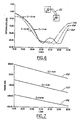
- FIGURE 6 is a graph of return loss versus frequency of three different unit cells in accordance with an embodiment of the present invention;
- FIGURE 7 is a graph of phase versus frequency of three unit cells in accordance with an embodiment of the present invention;
- FIGURE 8 is a graph of feed member length versus phase of three unit cells in accordance with an embodiment of the present invention; and
- FIGURE 9 is another embodiment of a unit cell.
-
- The present invention will be described in terms of its operation in a transmit mode. Due to the principle of reciprocity, the invention works the same in a reverse order for the receive mode. Referring to Figure 1, a
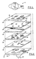
lens antenna structure 20 is preferred for use in asatellite 10 application as a result of its low profile and ease in which it can be configured to specialized geometries.Structure 20 is a horn-fed, multi-layered, printed circuit lens antenna particularly suited for shaped or pencil beams in the Ku and Ka bands. - Referring to Figure 2, one embodiment of the
lens antenna structure 20 is composed of a series of stacked layers. A firstdielectric layer 22 is positioned adjacent to afirst ground plane 24 which in turn is positioned adjacent to a seconddielectric layer 26. The seconddielectric layer 26 is positioned adjacent to a thirddielectric layer 28 which in turn is adjacent to asecond ground plane 30. Thesecond ground plane 30 is positioned adjacent to a fourthdielectric layer 32. - Interposed between the second
dielectric layer 26 and the thirddielectric layer 28 is afeed member plane 34. In addition, positioned on atop surface 36 of the firstdielectric layer 22 is afirst patch plane 38, and positioned on abottom surface 40 of the fourthdielectric layer 32 is asecond patch plane 42. In addition,slots second ground planes members 52 corresponding toslots dielectric layer 28. - In operation, the
feed members 52 capacitively and electromagnetically couple the first andsecond patch planes horn 44, remotely positioned below thesecond patch plane 42, emits electromagnetic energy in the direction of the antenna structure. This signal is received by thesecond patch plane 42, converted to TEM waves by theslots members 52 in theintermediate ground planes dielectric plane 28, and subsequently transmitted by thefirst patch plane 38. - Figure 3 is a top view of a
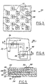
lens antenna structure 20 in accordance with one embodiment of the present invention. As shown in Figure 3, thelens antenna structure 20 comprises a plurality ofunit cells 46. Aunit cell 46 is shown in further detail in Figure 4. - As shown in Figure 4, each
unit cell 46 contains a portion of the layers and planes mentioned above. Eachunit cell 46 comprises afirst patch 48 from thefirst patch plane 38, atop slot 50 from thefirst ground plane 24, afeed member 52 from thefeed member plane 34, abottom slot 54 from thesecond ground plane 30, and asecond patch 56 from thesecond patch plane 42. Each of the elements comprising theunit cell 46 are separated by a dielectric substrate. - As shown in Figure 5,
patch 48 is separated fromslot 50 by thefirst dielectric layer 22;slot 50 is separated fromfeed member 52 by thesecond dielectric layer 26;feed member 52 is separated fromslot 54 by thethird dielectric layer 28; andslot 54 is separated from thesecond patch 56 by thefourth dielectric layer 32. - Referring again to Figure 4, the
first patch 48 is substantially centered over thetop slot 50, and thesecond patch 56 is centered beneath thebottom slot 54. Thefirst patch 48 is off-centered from thesecond patch 56. Thefeed member 52 has afirst end 58 positioned substantially perpendicular to thetop slot 50, and asecond end 60 positioned substantially perpendicular to thebottom slot 54. The feed member ends 58 and 60 extend to, and slightly beyond, theslots - In operation, the
second patch 56 receives electromagnetic energy from thehorn 44.Patch 56 radiates a frequency band centered at thesecond patch 56 resonance frequency. This radiation induces an electric field in thebottom slot 54 which extends transversely to the long dimension of theslot 54. This electric field creates a TEM wave which travels alongfeed member 52. This wave induces a second electric field in thetop slot 50 which, in turn, excitesfirst patch 48 at its resonating frequency.First patch 48 then transmits a frequency band centered about its resonating frequency. - The
feed member 52 can be configured in different shapes. For example, thefeed member 52 may be straight, so that the associatedtop slot 50 is parallel with the associatedbottom slot 54, or thefeed member 52 may be bent as shown in Figure 9. The preferred shape of thefeed member 52 is a shape which positions thefirst end 58 orthogonal to thesecond end 60. Such a feed member shape permits variations of feed member lengths from oneunit cell 46 to the next within the same array in a spacially efficient fashion. In addition, the orthogonal positioning of thefirst end 58 to thesecond end 60 simplifies manufacturing and reduces associated costs since the same patch plane pattern may be utilized for both thefirst patch plane 38 and thesecond patch plane 42. Likewise, the same ground plane pattern may be utilized for the first and second ground planes 24, 30. - Referring to Figure 6, "l" represents the distance from "s" to "s'" along the
feed member 52. The slot and patch dimensions are designed to provide good return loss. For example, with first and second patch dimensions of 0.5 cm x 0.5 cm, unit cell size of 0.88 cm x 0.88 cm, top and bottom slot size of 0.4 cm x 0.05 cm, first and fourth dielectric layer thicknesses of 0.1 cm with dielectric constant of 1.1, and second and third dielectric layer thicknesses of 0.038 cm with a dielectric constant of 2.53, the -15dB return loss bandwidth is approximately 10%. This is true whether l = 0.6 cm as shown inline 100, or l = 1.0 cm as shown inline 102, or l = 1.4 cm as shown in line 104. - As shown in Figure 7, the
feed member 52 propagates in the TEM mode, therefore the phase versus frequency characteristic of theunit cell 46 is linear (lines - The transmitted bandwidth can be increased by using thicker substrate for the first and fourth dielectric layers 22, 32 and/or using stacked
first patches 48. Preferably, the stacked patches are approximately equal in size so as to resonate at approximately the same frequencies, but differ enough so as to broaden the bandwidth. The dielectric substrate utilized between stacked patches will also cause broadening of the transmitted frequency bandwidth. The dielectric constant is higher for the second and thirddielectric layers first patch 48 and thesecond patch 56. Also, for a given off-set between thepatch 48 andpatch 56, a high dielectric substrate in the feed region provides a large dynamic range for the phase. - In order to generate shaped or pencil beams, the
lens antenna structure 20 must operate at appropriate phase differences. Phase differences are provided by varying the length of thefeed member 52 from oneunit cell 46 to the next. Figure 8 illustrates the phase shift versusfeed member 52 length for a representative frequency (line 110). - Figure 9 shows another embodiment of a unit cell. A dual polarization application can be configured when utilizing a
dual unit cell 62.Dual unit cell 62 is similar tounit cell 46 with anadditional feed member 52 coupled with additional top andbottom slots holes 64 plated with conductive metallic material connecting the respective ground planes in whichslots holes 64 is preferably less than 0.2 times the wavelength of the resonating frequency of the first andsecond patches - To sum up, the present invention relates to an antenna structure being formed of a first patch plane, a first ground plane, a feed member plane, a second ground plane, and a second patch plane all spaced apart by layers of laminated dielectric substrate. A horn transmits energy upon the second patch plane. The energy is controlled in terms of phase and frequency, and is further electromagnetically coupled to the first patch plane which transmits in the form of shaped or pencil beams. The coupling between patch planes is accomplished by an array of slots located through the ground planes and an array of feed members interposed between the ground planes. The phase differences are established by utilization of feed members with different lengths.
Claims (8)
- An antenna structure (20) comprising:a plurality of unit cells (46) each having:a first patch plane (38) having a first patch (48);a first ground plane (24) adjacent to said first patch plane (38), said first ground plane (24) having a top slot (50) in operative communication with said first patch (48); a first dielectric layer (22) interposed between said first patch plane (38) and said first ground plane (24);a feed member plane (34) adjacent to said first ground plane (24), said feed member plane (34) having a feed member (52) in operative communication with said top slot (50); a second dielectric layer (26) interposed between said first ground plane (24) and said feed member plane (34);a second ground plane (30) adjacent to said feed member plane (34); a third dielectric layer (28) interposed between said feed member plane (34) and said second ground plane (30); and characterised by: said second ground plane (30) having a bottom slot (54) in operative communication with said feed member (52);a second patch plane (42) adjacent to said second ground plane (30), said second patch plane (42) having a second patch (56) in operative communication with said bottom slot (54) and being adapted to receive electromagnetic energy from a horn (44); anda fourth dielectric layer (32) interposed between said second ground plane (30) and said second patch plane (42).
- The antenna structure (20) of Claim 1, characterized in that said feed member (52) has a first end (58) positioned perpendicular to and substantially under said top slot (50), and a second end (60) positioned perpendicular to and substantially over said bottom slot (54).
- The antenna structure (20) of Claim 1 or 2, characterized in that each unit cell of said plurality of unit cells (46) has said feed member (52) of varying lengths.
- The antenna structure (20) of Claim 2, characterized in that said first end (58) and said second end (60) are respectively positioned perpendicular to each other.
- The antenna structure (20) of any of Claims 1 to 4, characterized in that said first patch plane (38) and said second patch plane (42) are symmetrically identical, and said first ground plane (24) and said second ground plane (30) are symmetrically identical.
- The antenna structure (20) of any of claims 1 to 5, characterized in that said second dielectric layer (26) and said third dielectric layer (28) have a higher dielectric constant than said first dielectric layer (22) and said fourth dielectric layer (32).
- The satellite antenna structure (20) of any of claims 1 to 6, characterized in that each one of said plurality of unit cells (46) comprises a second feed member (52) and associated top and bottom slots (50, 54) wherein said feed members are separated by a plurality of holes (64) conductively plated and extending through said second dielectric layer (26) and said third dielectric layer (28) thereby connecting the first ground plane (24) with the second ground plane (30).
- The antenna structure (20) of any of Claims 1 to 7, characterized by a horn (44) for emitting energy upon said second patch plane (42).
Applications Claiming Priority (2)
| Application Number | Priority Date | Filing Date | Title |
|---|---|---|---|
| US220128 | 1980-12-24 | ||
| US09/220,128 US5990836A (en) | 1998-12-23 | 1998-12-23 | Multi-layered patch antenna |
Publications (2)
| Publication Number | Publication Date |
|---|---|
| EP1018778A1 EP1018778A1 (en) | 2000-07-12 |
| EP1018778B1 true EP1018778B1 (en) | 2003-04-02 |
Family
ID=22822189
Family Applications (1)
| Application Number | Title | Priority Date | Filing Date |
|---|---|---|---|
| EP99124675A Expired - Lifetime EP1018778B1 (en) | 1998-12-23 | 1999-12-10 | Multi-layered patch antenna |
Country Status (5)
| Country | Link |
|---|---|
| US (1) | US5990836A (en) |
| EP (1) | EP1018778B1 (en) |
| JP (1) | JP3314069B2 (en) |
| CA (1) | CA2292129C (en) |
| DE (1) | DE69906468T2 (en) |
Families Citing this family (16)
| Publication number | Priority date | Publication date | Assignee | Title |
|---|---|---|---|---|
| US6249439B1 (en) * | 1999-10-21 | 2001-06-19 | Hughes Electronics Corporation | Millimeter wave multilayer assembly |
| US6417806B1 (en) | 2001-01-31 | 2002-07-09 | Tantivy Communications, Inc. | Monopole antenna for array applications |
| US6369770B1 (en) | 2001-01-31 | 2002-04-09 | Tantivy Communications, Inc. | Closely spaced antenna array |
| US6396456B1 (en) | 2001-01-31 | 2002-05-28 | Tantivy Communications, Inc. | Stacked dipole antenna for use in wireless communications systems |
| US20030048226A1 (en) * | 2001-01-31 | 2003-03-13 | Tantivy Communications, Inc. | Antenna for array applications |
| US6369771B1 (en) | 2001-01-31 | 2002-04-09 | Tantivy Communications, Inc. | Low profile dipole antenna for use in wireless communications systems |
| GB2403069B8 (en) | 2003-06-16 | 2008-07-17 | Antenova Ltd | Hybrid antenna using parasiting excitation of conducting antennas by dielectric antennas |
| US7071879B2 (en) * | 2004-06-01 | 2006-07-04 | Ems Technologies Canada, Ltd. | Dielectric-resonator array antenna system |
| JP2006029834A (en) * | 2004-07-13 | 2006-02-02 | Hitachi Ltd | Vehicle-mounted radar |
| US7098854B2 (en) * | 2004-09-09 | 2006-08-29 | Raytheon Company | Reflect antenna |
| US7656345B2 (en) | 2006-06-13 | 2010-02-02 | Ball Aerospace & Technoloiges Corp. | Low-profile lens method and apparatus for mechanical steering of aperture antennas |
| US7595760B2 (en) * | 2006-08-04 | 2009-09-29 | Raytheon Company | Airship mounted array |
| US7605767B2 (en) * | 2006-08-04 | 2009-10-20 | Raytheon Company | Space-fed array operable in a reflective mode and in a feed-through mode |
| US7800542B2 (en) * | 2008-05-23 | 2010-09-21 | Agc Automotive Americas R&D, Inc. | Multi-layer offset patch antenna |
| KR101744605B1 (en) * | 2012-11-07 | 2017-06-08 | 가부시키가이샤 무라타 세이사쿠쇼 | Array antenna |
| KR20210138418A (en) * | 2020-05-12 | 2021-11-19 | 삼성전자주식회사 | Antenna module and electronic device including the same |
Family Cites Families (5)
| Publication number | Priority date | Publication date | Assignee | Title |
|---|---|---|---|---|
| JP2846081B2 (en) * | 1990-07-25 | 1999-01-13 | 日立化成工業株式会社 | Triplate type planar antenna |
| JPH0567912A (en) * | 1991-04-24 | 1993-03-19 | Matsushita Electric Works Ltd | Flat antenna |
| DE4239597C2 (en) * | 1991-11-26 | 1999-11-04 | Hitachi Chemical Co Ltd | Flat antenna with dual polarization |
| US5394163A (en) * | 1992-08-26 | 1995-02-28 | Hughes Missile Systems Company | Annular slot patch excited array |
| US5661494A (en) * | 1995-03-24 | 1997-08-26 | The United States Of America As Represented By The Administrator Of The National Aeronautics And Space Administration | High performance circularly polarized microstrip antenna |
-
1998
- 1998-12-23 US US09/220,128 patent/US5990836A/en not_active Expired - Lifetime
-
1999
- 1999-12-10 EP EP99124675A patent/EP1018778B1/en not_active Expired - Lifetime
- 1999-12-10 DE DE69906468T patent/DE69906468T2/en not_active Expired - Lifetime
- 1999-12-13 CA CA002292129A patent/CA2292129C/en not_active Expired - Lifetime
- 1999-12-22 JP JP36437199A patent/JP3314069B2/en not_active Expired - Lifetime
Also Published As
| Publication number | Publication date |
|---|---|
| US5990836A (en) | 1999-11-23 |
| CA2292129C (en) | 2002-04-23 |
| DE69906468D1 (en) | 2003-05-08 |
| JP2000196347A (en) | 2000-07-14 |
| DE69906468T2 (en) | 2003-10-30 |
| JP3314069B2 (en) | 2002-08-12 |
| EP1018778A1 (en) | 2000-07-12 |
| CA2292129A1 (en) | 2000-06-23 |
Similar Documents
| Publication | Publication Date | Title |
|---|---|---|
| EP0447218B1 (en) | Plural frequency patch antenna assembly | |
| US5070340A (en) | Broadband microstrip-fed antenna | |
| EP0972317B1 (en) | Microstrip array antenna | |
| EP0449492B1 (en) | Patch antenna with polarization uniformity control | |
| US5382959A (en) | Broadband circular polarization antenna | |
| US4812855A (en) | Dipole antenna with parasitic elements | |
| US6535169B2 (en) | Source antennas for transmitting/receiving electromagnetic waves for satellite telecommunications systems | |
| US4929959A (en) | Dual-polarized printed circuit antenna having its elements capacitively coupled to feedlines | |
| US6545647B1 (en) | Antenna system for communicating simultaneously with a satellite and a terrestrial system | |
| US4710775A (en) | Parasitically coupled, complementary slot-dipole antenna element | |
| EP1647072B1 (en) | Wideband phased array radiator | |
| US7705782B2 (en) | Microstrip array antenna | |
| EP1018778B1 (en) | Multi-layered patch antenna | |
| KR0184529B1 (en) | Slot-coupled fed dual circular polarization tem mode slot array antenna | |
| JPH09326631A (en) | Microwave planar array antenna | |
| KR20030091383A (en) | Planar antenna with circular and linear polarization. | |
| CN100365866C (en) | Patch dipole array antenna including feed line organizer body and related methods | |
| US5633646A (en) | Mini-cap radiating element | |
| US5233364A (en) | Dual-polarized microwave antenna element | |
| Baghel et al. | SICL fed Ka-band dual polarized dipole antenna array for 5G endfire application | |
| JPH0590826A (en) | Microstrip antenna | |
| Abd El-Rahman et al. | Dual-Band Cavity-Backed KA-band antenna for satellite communication | |
| CN1985406A (en) | Microstrip array antenna | |
| CN118315815B (en) | Cross-frequency-band double-circular polarization fusion antenna based on F-P resonant cavity |
Legal Events
| Date | Code | Title | Description |
|---|---|---|---|
| PUAI | Public reference made under article 153(3) epc to a published international application that has entered the european phase |
Free format text: ORIGINAL CODE: 0009012 |
|
| AK | Designated contracting states |
Kind code of ref document: A1 Designated state(s): DE FR GB IT |
|
| AX | Request for extension of the european patent |
Free format text: AL;LT;LV;MK;RO;SI |
|
| 17P | Request for examination filed |
Effective date: 20001214 |
|
| AKX | Designation fees paid |
Free format text: DE FR GB IT |
|
| 17Q | First examination report despatched |
Effective date: 20010907 |
|
| GRAG | Despatch of communication of intention to grant |
Free format text: ORIGINAL CODE: EPIDOS AGRA |
|
| GRAG | Despatch of communication of intention to grant |
Free format text: ORIGINAL CODE: EPIDOS AGRA |
|
| GRAH | Despatch of communication of intention to grant a patent |
Free format text: ORIGINAL CODE: EPIDOS IGRA |
|
| GRAH | Despatch of communication of intention to grant a patent |
Free format text: ORIGINAL CODE: EPIDOS IGRA |
|
| GRAA | (expected) grant |
Free format text: ORIGINAL CODE: 0009210 |
|
| AK | Designated contracting states |
Designated state(s): DE FR GB IT |
|
| REG | Reference to a national code |
Ref country code: GB Ref legal event code: FG4D |
|
| REF | Corresponds to: |
Ref document number: 69906468 Country of ref document: DE Date of ref document: 20030508 Kind code of ref document: P |
|
| ET | Fr: translation filed | ||
| PLBE | No opposition filed within time limit |
Free format text: ORIGINAL CODE: 0009261 |
|
| STAA | Information on the status of an ep patent application or granted ep patent |
Free format text: STATUS: NO OPPOSITION FILED WITHIN TIME LIMIT |
|
| 26N | No opposition filed |
Effective date: 20040105 |
|
| REG | Reference to a national code |
Ref country code: FR Ref legal event code: PLFP Year of fee payment: 17 |
|
| REG | Reference to a national code |
Ref country code: FR Ref legal event code: PLFP Year of fee payment: 18 |
|
| PG25 | Lapsed in a contracting state [announced via postgrant information from national office to epo] |
Ref country code: IT Free format text: LAPSE BECAUSE OF NON-PAYMENT OF DUE FEES Effective date: 20151210 |
|
| PG25 | Lapsed in a contracting state [announced via postgrant information from national office to epo] |
Ref country code: IT Free format text: LAPSE BECAUSE OF NON-PAYMENT OF DUE FEES Effective date: 20151210 |
|
| PGRI | Patent reinstated in contracting state [announced from national office to epo] |
Ref country code: IT Effective date: 20170710 |
|
| REG | Reference to a national code |
Ref country code: FR Ref legal event code: PLFP Year of fee payment: 19 |
|
| PGFP | Annual fee paid to national office [announced via postgrant information from national office to epo] |
Ref country code: FR Payment date: 20181226 Year of fee payment: 20 Ref country code: GB Payment date: 20181227 Year of fee payment: 20 |
|
| PGFP | Annual fee paid to national office [announced via postgrant information from national office to epo] |
Ref country code: DE Payment date: 20181231 Year of fee payment: 20 Ref country code: IT Payment date: 20181220 Year of fee payment: 20 |
|
| REG | Reference to a national code |
Ref country code: DE Ref legal event code: R071 Ref document number: 69906468 Country of ref document: DE |
|
| REG | Reference to a national code |
Ref country code: GB Ref legal event code: PE20 Expiry date: 20191209 |
|
| PG25 | Lapsed in a contracting state [announced via postgrant information from national office to epo] |
Ref country code: GB Free format text: LAPSE BECAUSE OF EXPIRATION OF PROTECTION Effective date: 20191209 |