EP1018164B1 - Silicon carbide static induction transistor structure - Google Patents
Silicon carbide static induction transistor structure Download PDFInfo
- Publication number
- EP1018164B1 EP1018164B1 EP98928829A EP98928829A EP1018164B1 EP 1018164 B1 EP1018164 B1 EP 1018164B1 EP 98928829 A EP98928829 A EP 98928829A EP 98928829 A EP98928829 A EP 98928829A EP 1018164 B1 EP1018164 B1 EP 1018164B1
- Authority
- EP
- European Patent Office
- Prior art keywords
- layer
- gate regions
- silicon carbide
- source
- regions
- Prior art date
- Legal status (The legal status is an assumption and is not a legal conclusion. Google has not performed a legal analysis and makes no representation as to the accuracy of the status listed.)
- Expired - Lifetime
Links
- HBMJWWWQQXIZIP-UHFFFAOYSA-N silicon carbide Chemical compound [Si+]#[C-] HBMJWWWQQXIZIP-UHFFFAOYSA-N 0.000 title claims abstract description 37
- 229910010271 silicon carbide Inorganic materials 0.000 title claims abstract description 37
- 230000006698 induction Effects 0.000 title claims abstract description 23
- 230000003068 static effect Effects 0.000 title claims abstract description 23
- 239000000758 substrate Substances 0.000 claims abstract description 30
- 150000002500 ions Chemical class 0.000 abstract description 7
- 230000009977 dual effect Effects 0.000 abstract 1
- XUIMIQQOPSSXEZ-UHFFFAOYSA-N Silicon Chemical compound [Si] XUIMIQQOPSSXEZ-UHFFFAOYSA-N 0.000 description 12
- 230000005684 electric field Effects 0.000 description 12
- 229910052710 silicon Inorganic materials 0.000 description 12
- 239000010703 silicon Substances 0.000 description 12
- 230000000903 blocking effect Effects 0.000 description 10
- 230000015556 catabolic process Effects 0.000 description 10
- 238000000034 method Methods 0.000 description 9
- 238000001465 metallisation Methods 0.000 description 8
- 239000002019 doping agent Substances 0.000 description 7
- 230000001681 protective effect Effects 0.000 description 5
- XKRFYHLGVUSROY-UHFFFAOYSA-N Argon Chemical compound [Ar] XKRFYHLGVUSROY-UHFFFAOYSA-N 0.000 description 4
- PXHVJJICTQNCMI-UHFFFAOYSA-N Nickel Chemical compound [Ni] PXHVJJICTQNCMI-UHFFFAOYSA-N 0.000 description 4
- 238000000151 deposition Methods 0.000 description 4
- 230000008021 deposition Effects 0.000 description 4
- 238000005468 ion implantation Methods 0.000 description 4
- 229910052751 metal Inorganic materials 0.000 description 3
- 239000002184 metal Substances 0.000 description 3
- 239000004065 semiconductor Substances 0.000 description 3
- IJGRMHOSHXDMSA-UHFFFAOYSA-N Atomic nitrogen Chemical compound N#N IJGRMHOSHXDMSA-UHFFFAOYSA-N 0.000 description 2
- VYPSYNLAJGMNEJ-UHFFFAOYSA-N Silicium dioxide Chemical compound O=[Si]=O VYPSYNLAJGMNEJ-UHFFFAOYSA-N 0.000 description 2
- 239000000956 alloy Substances 0.000 description 2
- 229910045601 alloy Inorganic materials 0.000 description 2
- 229910052782 aluminium Inorganic materials 0.000 description 2
- 229910052786 argon Inorganic materials 0.000 description 2
- 238000009792 diffusion process Methods 0.000 description 2
- 238000004519 manufacturing process Methods 0.000 description 2
- 229910052759 nickel Inorganic materials 0.000 description 2
- 229920006395 saturated elastomer Polymers 0.000 description 2
- ZOXJGFHDIHLPTG-UHFFFAOYSA-N Boron Chemical compound [B] ZOXJGFHDIHLPTG-UHFFFAOYSA-N 0.000 description 1
- RTAQQCXQSZGOHL-UHFFFAOYSA-N Titanium Chemical compound [Ti] RTAQQCXQSZGOHL-UHFFFAOYSA-N 0.000 description 1
- XAGFODPZIPBFFR-UHFFFAOYSA-N aluminium Chemical compound [Al] XAGFODPZIPBFFR-UHFFFAOYSA-N 0.000 description 1
- -1 aluminum ions Chemical class 0.000 description 1
- 230000004888 barrier function Effects 0.000 description 1
- 229910052796 boron Inorganic materials 0.000 description 1
- 239000000969 carrier Substances 0.000 description 1
- 238000010276 construction Methods 0.000 description 1
- 230000001419 dependent effect Effects 0.000 description 1
- 230000001627 detrimental effect Effects 0.000 description 1
- 238000009429 electrical wiring Methods 0.000 description 1
- 238000005421 electrostatic potential Methods 0.000 description 1
- 238000005530 etching Methods 0.000 description 1
- 230000005669 field effect Effects 0.000 description 1
- 239000001257 hydrogen Substances 0.000 description 1
- 229910052739 hydrogen Inorganic materials 0.000 description 1
- 238000002513 implantation Methods 0.000 description 1
- 239000012535 impurity Substances 0.000 description 1
- 239000012212 insulator Substances 0.000 description 1
- 230000000873 masking effect Effects 0.000 description 1
- 239000000463 material Substances 0.000 description 1
- 239000000203 mixture Substances 0.000 description 1
- 229910052757 nitrogen Inorganic materials 0.000 description 1
- 230000010355 oscillation Effects 0.000 description 1
- 238000004806 packaging method and process Methods 0.000 description 1
- 230000002028 premature Effects 0.000 description 1
- 230000001698 pyrogenic effect Effects 0.000 description 1
- 235000012239 silicon dioxide Nutrition 0.000 description 1
- 239000000377 silicon dioxide Substances 0.000 description 1
- 239000002470 thermal conductor Substances 0.000 description 1
- 239000010936 titanium Substances 0.000 description 1
- 229910052719 titanium Inorganic materials 0.000 description 1
- 230000007704 transition Effects 0.000 description 1
- 238000000927 vapour-phase epitaxy Methods 0.000 description 1
Images


Classifications
-
- H—ELECTRICITY
- H01—ELECTRIC ELEMENTS
- H01L—SEMICONDUCTOR DEVICES NOT COVERED BY CLASS H10
- H01L29/00—Semiconductor devices adapted for rectifying, amplifying, oscillating or switching, or capacitors or resistors with at least one potential-jump barrier or surface barrier, e.g. PN junction depletion layer or carrier concentration layer; Details of semiconductor bodies or of electrodes thereof ; Multistep manufacturing processes therefor
- H01L29/66—Types of semiconductor device ; Multistep manufacturing processes therefor
- H01L29/68—Types of semiconductor device ; Multistep manufacturing processes therefor controllable by only the electric current supplied, or only the electric potential applied, to an electrode which does not carry the current to be rectified, amplified or switched
- H01L29/76—Unipolar devices, e.g. field effect transistors
- H01L29/772—Field effect transistors
- H01L29/7722—Field effect transistors using static field induced regions, e.g. SIT, PBT
-
- H—ELECTRICITY
- H01—ELECTRIC ELEMENTS
- H01L—SEMICONDUCTOR DEVICES NOT COVERED BY CLASS H10
- H01L29/00—Semiconductor devices adapted for rectifying, amplifying, oscillating or switching, or capacitors or resistors with at least one potential-jump barrier or surface barrier, e.g. PN junction depletion layer or carrier concentration layer; Details of semiconductor bodies or of electrodes thereof ; Multistep manufacturing processes therefor
- H01L29/66—Types of semiconductor device ; Multistep manufacturing processes therefor
- H01L29/66007—Multistep manufacturing processes
- H01L29/66053—Multistep manufacturing processes of devices having a semiconductor body comprising crystalline silicon carbide
- H01L29/66068—Multistep manufacturing processes of devices having a semiconductor body comprising crystalline silicon carbide the devices being controllable only by the electric current supplied or the electric potential applied, to an electrode which does not carry the current to be rectified, amplified or switched, e.g. three-terminal devices
-
- H—ELECTRICITY
- H01—ELECTRIC ELEMENTS
- H01L—SEMICONDUCTOR DEVICES NOT COVERED BY CLASS H10
- H01L29/00—Semiconductor devices adapted for rectifying, amplifying, oscillating or switching, or capacitors or resistors with at least one potential-jump barrier or surface barrier, e.g. PN junction depletion layer or carrier concentration layer; Details of semiconductor bodies or of electrodes thereof ; Multistep manufacturing processes therefor
- H01L29/02—Semiconductor bodies ; Multistep manufacturing processes therefor
- H01L29/06—Semiconductor bodies ; Multistep manufacturing processes therefor characterised by their shape; characterised by the shapes, relative sizes, or dispositions of the semiconductor regions ; characterised by the concentration or distribution of impurities within semiconductor regions
- H01L29/0603—Semiconductor bodies ; Multistep manufacturing processes therefor characterised by their shape; characterised by the shapes, relative sizes, or dispositions of the semiconductor regions ; characterised by the concentration or distribution of impurities within semiconductor regions characterised by particular constructional design considerations, e.g. for preventing surface leakage, for controlling electric field concentration or for internal isolations regions
- H01L29/0607—Semiconductor bodies ; Multistep manufacturing processes therefor characterised by their shape; characterised by the shapes, relative sizes, or dispositions of the semiconductor regions ; characterised by the concentration or distribution of impurities within semiconductor regions characterised by particular constructional design considerations, e.g. for preventing surface leakage, for controlling electric field concentration or for internal isolations regions for preventing surface leakage or controlling electric field concentration
- H01L29/0611—Semiconductor bodies ; Multistep manufacturing processes therefor characterised by their shape; characterised by the shapes, relative sizes, or dispositions of the semiconductor regions ; characterised by the concentration or distribution of impurities within semiconductor regions characterised by particular constructional design considerations, e.g. for preventing surface leakage, for controlling electric field concentration or for internal isolations regions for preventing surface leakage or controlling electric field concentration for increasing or controlling the breakdown voltage of reverse biased devices
- H01L29/0615—Semiconductor bodies ; Multistep manufacturing processes therefor characterised by their shape; characterised by the shapes, relative sizes, or dispositions of the semiconductor regions ; characterised by the concentration or distribution of impurities within semiconductor regions characterised by particular constructional design considerations, e.g. for preventing surface leakage, for controlling electric field concentration or for internal isolations regions for preventing surface leakage or controlling electric field concentration for increasing or controlling the breakdown voltage of reverse biased devices by the doping profile or the shape or the arrangement of the PN junction, or with supplementary regions, e.g. junction termination extension [JTE]
- H01L29/0619—Semiconductor bodies ; Multistep manufacturing processes therefor characterised by their shape; characterised by the shapes, relative sizes, or dispositions of the semiconductor regions ; characterised by the concentration or distribution of impurities within semiconductor regions characterised by particular constructional design considerations, e.g. for preventing surface leakage, for controlling electric field concentration or for internal isolations regions for preventing surface leakage or controlling electric field concentration for increasing or controlling the breakdown voltage of reverse biased devices by the doping profile or the shape or the arrangement of the PN junction, or with supplementary regions, e.g. junction termination extension [JTE] with a supplementary region doped oppositely to or in rectifying contact with the semiconductor containing or contacting region, e.g. guard rings with PN or Schottky junction
-
- H—ELECTRICITY
- H01—ELECTRIC ELEMENTS
- H01L—SEMICONDUCTOR DEVICES NOT COVERED BY CLASS H10
- H01L29/00—Semiconductor devices adapted for rectifying, amplifying, oscillating or switching, or capacitors or resistors with at least one potential-jump barrier or surface barrier, e.g. PN junction depletion layer or carrier concentration layer; Details of semiconductor bodies or of electrodes thereof ; Multistep manufacturing processes therefor
- H01L29/02—Semiconductor bodies ; Multistep manufacturing processes therefor
- H01L29/06—Semiconductor bodies ; Multistep manufacturing processes therefor characterised by their shape; characterised by the shapes, relative sizes, or dispositions of the semiconductor regions ; characterised by the concentration or distribution of impurities within semiconductor regions
- H01L29/0684—Semiconductor bodies ; Multistep manufacturing processes therefor characterised by their shape; characterised by the shapes, relative sizes, or dispositions of the semiconductor regions ; characterised by the concentration or distribution of impurities within semiconductor regions characterised by the shape, relative sizes or dispositions of the semiconductor regions or junctions between the regions
- H01L29/0692—Surface layout
- H01L29/0696—Surface layout of cellular field-effect devices, e.g. multicellular DMOS transistors or IGBTs
-
- H—ELECTRICITY
- H01—ELECTRIC ELEMENTS
- H01L—SEMICONDUCTOR DEVICES NOT COVERED BY CLASS H10
- H01L29/00—Semiconductor devices adapted for rectifying, amplifying, oscillating or switching, or capacitors or resistors with at least one potential-jump barrier or surface barrier, e.g. PN junction depletion layer or carrier concentration layer; Details of semiconductor bodies or of electrodes thereof ; Multistep manufacturing processes therefor
- H01L29/02—Semiconductor bodies ; Multistep manufacturing processes therefor
- H01L29/12—Semiconductor bodies ; Multistep manufacturing processes therefor characterised by the materials of which they are formed
- H01L29/16—Semiconductor bodies ; Multistep manufacturing processes therefor characterised by the materials of which they are formed including, apart from doping materials or other impurities, only elements of Group IV of the Periodic System
- H01L29/1608—Silicon carbide
-
- H—ELECTRICITY
- H01—ELECTRIC ELEMENTS
- H01L—SEMICONDUCTOR DEVICES NOT COVERED BY CLASS H10
- H01L29/00—Semiconductor devices adapted for rectifying, amplifying, oscillating or switching, or capacitors or resistors with at least one potential-jump barrier or surface barrier, e.g. PN junction depletion layer or carrier concentration layer; Details of semiconductor bodies or of electrodes thereof ; Multistep manufacturing processes therefor
- H01L29/02—Semiconductor bodies ; Multistep manufacturing processes therefor
- H01L29/30—Semiconductor bodies ; Multistep manufacturing processes therefor characterised by physical imperfections; having polished or roughened surface
- H01L29/32—Semiconductor bodies ; Multistep manufacturing processes therefor characterised by physical imperfections; having polished or roughened surface the imperfections being within the semiconductor body
Definitions
- the invention in general relates to semiconductor structures, and more particularly to a silicon carbide static induction transistor capable of high frequency, high power operation.
- a typical static induction transistor is a vertical structure device wherein active carriers flow from a source region to a drain region on opposite sides of a substrate member. Current flowing from source to drain is controlled by an electrostatic potential barrier induced by gate regions positioned on either side of the source region.
- the static induction transistor has a d.c. current-voltage characteristic similar to a vacuum tube triode and is relatively linear over a wide range of drain current values.
- Static induction transistors are typically made of silicon and can operate at frequencies up to approximately 1 GHz and can handle maximum power densities of less than about 12 kW/cm 2 .
- a plurality of such static induction transistors are generally interconnected in an array to provide a desired function such as a radar transmitter.
- the present invention provides for such need with a device operable at the higher frequencies and power levels desired. This is accomplished with fewer transistors accommodated within a smaller package than comparable silicon static induction devices providing the same function.
- US-A-5612547 relates to static induction transistors in which a silicon carbide substrate is provided. A silicon carbide drift layer is provided on the substrate. However, the exact geometric dimensions defined by the present invention are not disclosed.
- WO 96/01500 describes silicon carbide field-effect transistors with source, gate and drain contacts, in which the source contacts are located on the surface of the semiconductor wafer.
- the geometry proposed and defined by the present invention, however, is not disclosed.
- JP-A2-1291462 discloses a method of producing silicon carbide transistor structures having a plurality of guard rings surrounding gate regions.
- a static induction transistor in accordance with the present invention is set out in claim 1. Specific embodiments are defined in the dependent claims.
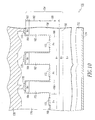
- Fig. 1 represents a portion of a conventional silicon static induction transistor having an n + substrate 12, defining a drain region for collecting electrons, and upon which is deposited an n - layer 14.
- n + substrate 12 Formed within the layer 14, by diffusion techniques are a plurality of n + source regions 16, extending perpendicular to the plane of the Fig., for supplying electrons, and being in an alternating relationship with a plurality of p + gate regions 18, also extending perpendicular to the plane of the Fig.
- a thick oxide layer 20 covering layer 14 has a series of windows formed therethrough for making electrical contact with the source and drain regions by means of commonly connected metal source contacts 22 and commonly connected metal gate contacts 24.
- a metal drain contact 26 is also provided and covers the surface of substrate 12 opposite layer 14.
- each pair of gate regions 18 on either side of a source region 16 modulate the flow of electrons through a vertical region 30, after which the electrons drift to the drain 12, through a drift layer 32, in a current profile roughly depicted by numeral 34.
- a typical silicon static induction transistor as illustrated in Fig. 1 has a drift layer thickness d of at least 10 ⁇ m (microns) or greater and a pitch p, or distance between gate regions, of at least 7 ⁇ m.
- Critical performance parameters as applied to static induction transistors include on-state current maximum, I max , blocking voltage, V block , cut-off frequency, f t , and maximum frequency of oscillation, f max .
- the first two parameters determine the output power of the device at the operating frequency and the last two parameters determine the useable frequency range.
- the current I max is inversely proportional to the thickness d of the drift layer, as is the cut-off frequency f t whereas the blocking voltage is directly proportional to the thickness of the drift layer and the breakdown critical field of the semiconductor material.
- A is the minimum cross-sectional area of the current flow
- q is the electron charge
- N d is the doping density in the drift layer 32
- ⁇ n is the electron mobility
- V D is the drain voltage bias
- d is the thickness of the drift layer 32
- E c is the critical electric field
- V sat is the saturated drift velocity.
- the blocking voltage is the maximum voltage that can be applied between source and drain before excessive current flows, due to breakdown phenomena.
- a relatively high blocking voltage is desired for greater output power at a given frequency, and from equation (2) this may be accomplished by increasing the thickness d of the drift layer. Increasing d, however, from equation (1), reduces the maximum current I max . From TABLE 1 and equation (2) it may be seen that for the same blocking voltage, the drift layer thickness d for silicon carbide may theoretically be 10 times thinner than for silicon due to the difference in critical breakdown fields (3.0 vs 0.3 MV/cm). A thinner drift layer in the silicon carbide will allow for a greater maximum current as well as a higher cut-off frequency, f t as set out in equation (3).
- the term in parenthesis in equation (5) is 5 times higher for silicon carbide than for silicon (2100 vs 420) so that the power per unit area is greater, thus allowing for smaller packaging requirements with fewer transistors.
- the thermal conductivity of the silicon carbide aids in removing excess heat generated at these higher powers.
- FIG. 2 A silicon carbide transistor structure, in accordance with one embodiment of the present invention, is illustrated in Figs 2 and 3 .
- Fig. 2 showing the transistor structure 40 in an early stage of fabrication, includes an n + substrate member 42 of silicon carbide.
- the silicon carbide substrate may be a 4H polytype as well as other polytypes including, but not limited to, the 3C, 2H, 6H and 15R polytypes.
- a silicon carbide layer arrangement 44 having one or more layers, is deposited upon the substrate 42 by epitaxial growth techniques such as vapor phase epitaxy during which process intentional impurity atoms of a dopant are added, as desired, to produce layers with predetermined dopant levels and conductivities.
- the substrate member 42 cut from a grown silicon carbide boule, generally will have slight imperfections in its surface which could lead to a breakdown during transistor operation. Accordingly, a silicon carbide n + buffer layer 46 may be deposited to provide a transition from a relatively high electric field in the drift layer to a relatively low electric field in the substrate 42.
- the next two layers are constituted by a silicon carbide n - layer 48, which will contain a drift layer, and a silicon carbide n + top layer 50 which has the highest dopant level of all the layers and from which will be formed the source regions of the transistor.
- buffer layer 46 grown to a thickness of about 0.5 ⁇ m, has a dopant level of 1x10 18 cm -3 (atoms per cubic centimeter).
- Layer 48 grown to a thickness of about 1.25 to 6.5 ⁇ m, has a dopant level of 1x10 15 to 2x10 16 cm -3
- top layer 50 grown to a thickness of about 0.5 ⁇ m, has a dopant level of 1x10 20 to 5x10 20 cm -3 .
- the dopant for these epitaxial layers may be nitrogen.
- portions 52 of layer 50 are removed, as is about 100 nm of layer 48, leaving a plurality of spaced apart portions 54 which extend as fingers perpendicular to the plane of the Fig. and which will form the source regions of the completed transistor structure.
- the completed transistor structure 40 includes a plurality of spaced apart p + gate regions 60 alternating laterally with source regions 54, and also extending as fingers perpendicular to the plane of the Fig.
- Gate regions 60 are not formed by diffusion, as is done in silicon, because the process would require detrimental temperatures in excess of 2000° C. Accordingly, gate regions 60, of width w, are formed within layer 48 by means of a series of ion implantation steps, with for example, boron or aluminum ions. The implantation is carried out at various energy levels and to a depth g of about 0.25 to 1.5 ⁇ m. With the source and gate regions as illustrated, the substrate 42 then functions as the drain for the transistor.
- a protective thermal oxide 62 such as high quality silicon dioxide is grown by a pyrogenic method over the exposed surface of the structure at a temperature of about 1150°C for 2 hours and annealed in argon for 30 minutes. Thereafter the protective oxide 62 is selectively removed to allow for the deposition of source contacts 64, gate contacts 66 and drain contact 68.
- source contacts 64, gate contacts 66 and drain contact 68 may be nickel, by way of example.
- the structure is then annealed in an argon-hydrogen mixture at 1150° C for a couple of minutes to form an alloy with nickel and elements in the silicon carbide regions 54.
- For the gate contacts multiple stacks of aluminum/titanium layers may be deposited and thereafter annealed to alloy the metalization.
- a relatively thick oxide layer for example 1 ⁇ m, is desired to act as a field insulator.
- the protective oxide 62 is grown to a thickness of about 50 nm in a 2 hour period. To continue such growth to a thickness of 1 ⁇ m would consume an excessive amount of time.
- a second, and low temperature oxide layer 70 is deposited, as opposed to grown, upon thermal oxide layer 62 to a thickness of about 950 nm. Windows are then formed in the thick oxide layer 70 to allow for common electrical connection to a metalization layer 72, for the source contacts 64, thereby forming a single source connection.
- a similar metalization layer is provided for the gate contacts 66, however it is located at the distal ends of the gate regions, out of the plane of the Fig.
- a region 76 of thickness h, wherein electrons supplied by the source region are modulated, is defined between the gate regions 60, and a drift layer 78 of thickness d is defined by the minimum distance between a gate region 60 and the drain 42. If a buffer layer such as 46 is provided, the drift layer would extend to the top of that layer, as illustrated.
- the drift layer has a thickness d of 1 to 5 ⁇ m resulting in a blocking voltage value, as defined in equation (2), equal to that of a silicon static induction transistor having an order of magnitude thicker drift layer of 10 to 50 ⁇ m.
- the thinner drift layer presents less resistance and allows for a greater maximum current to flow through the device.
- the distance between gate regions 60, from center to center is designated by the pitch p.
- the present invention allows for a smaller pitch than conventional static induction transistors and by way of example to understand the present invention p is in the range of about 1 to 5 ⁇ m.
- the gate regions 60 are illustrated in idealized form. In actuality, the ion implanted regions may curve or bulge at the lower end thereof.
- Width y defined as the minimum distance between gate regions 60, ranges, by way of example to understand the present invention, from about 0.5 to 3.0 ⁇ m and the thickness h of region 76, which is the maximum vertical distance between a source and gate region, ranges from 0.25 to 1.5 ⁇ m. Otherwise stated, the ratio of y/h ranges from 1 to 2.
- Fig. 3A The relationship between these values is illustrated in Fig. 3A wherein the thickness h of region 76 is plotted on the horizontal axis and the gap, or width y between gate regions 60, is plotted on the vertical axis.
- the transistor structure may be fabricated with dimensions as defined by the shaded area 84 between the curves 80 and 82. In general, with a smaller gap distance y the gate regions exert more control over the current than does the drain, and higher gain is achievable for the same bias conditions.
- the substrate 42 also acts as a support for the silicon carbide epitaxial layers deposited thereon.
- the thickness of a typical silicon carbide substrate 42 may range from about 250 to 350 ⁇ m.
- the electrical resistance of a relatively thick substrate tends to limit the power efficiency of the transistor and accordingly, it is desired to make the substrate as thin as practical, both from an electrical standpoint as well as a thermal standpoint.
- Fig. 4 illustrating an example of a transitor structure.
- a drain contact is positioned on the same side of a substrate member as the source and gate contacts. More particularly, a drain contact 86, formed through a window in thermal oxide layer 62 and deposited oxide layer 70, surrounds the source and gate finger arrangement and makes electrical contact with the substrate member 42'. A metalization layer 88 may then be applied over the oxide layer 70 for electrical connection to the drain contact 86. With this design, the substrate may be much thinner than the substrate 42 illustrated in Fig. 3 and can be bonded to a thermal conductor 90, whereby heat generated during operation may be efficiently extracted, resulting in better thermal management.
- the current which essentially flows vertically through layer 48 now only has to flow a short distance (tens of ⁇ m) transversely to the surrounding drain contact 86 instead of through the substrate (hundreds of ⁇ m).
- the total distance traveled by the electrons may be 10 times less with the arrangement of Fig. 4 , and as such, less heat is generated during operation.
- the vertical distance h of region 76 between the source and bottom of the gate region should be at least 0.25 to 1.5 ⁇ m to obtain reasonable voltage gain, for example, greater than 10.
- the pitch p is reduced to ⁇ 2 ⁇ m, whereby the width y may be reduced to the range of 0.3 to 1.5 ⁇ m, with the thickness h then having a corresponding range of 0.15 to 1.2 ⁇ m, in accordance with the curves of Fig. 3A .
- an implanted source region as illustrated in Fig. 5 may be employed.
- the transistor structure 100 includes an n + silicon carbide substrate 102 and a silicon carbide layer arrangement 103, which includes an n + buffer layer 104 and an n - layer 106, both deposited by techniques previously described.
- P + gate regions 108 are formed by ion implantation to a depth g and n + source regions 110, alternating laterally with gate regions 108, are also formed by ion implantation into layer 106.
- the ion implanted gate and source regions 108 and 110 define, in layer 106, a region 112 of thickness h, the maximum vertical distance between a source and gate region.
- the gap or width y should be no more than 0.5 ⁇ m and no less than 0.25 ⁇ m for satisfactory operation. If the device is fabricated with a thickness h of 0.5 ⁇ m for region 112, then the width y should be no more than 1.0 ⁇ m and no less than 0.5 ⁇ m.
- the drift layer 114 as before, ranges from 1 to 5 ⁇ m.
- the transistor structure 100 includes a grown thermal protective oxide 116 through which portions are selectively removed for deposition of respective source, gate and drain contacts 118, 120 and 122. Covering the thermal oxide 116 is a deposited oxide layer 124 having windows for making electrical connection of a metalization layer 126 with source contacts 118. A similar metalization layer is provided for the gate contacts, however it is located at the distal ends of the gate regions, out of the plane of the Figure.
- Fig. 6 duplicates the transistor structure of Fig. 3 and illustrates a plurality of equipotential field lines 130 which exist during operation. It is desired that the transistor device have as high a blocking voltage as possible since more power can then be output at a particular frequency.
- the blocking voltage is a function of drift layer distance d as well as critical breakdown field E c , listed in TABLE 1.
- the actual value for E c is reduced however by the excessive electric field concentration at the edge gate region 60' in area 132 which causes a premature breakdown at the gate-drift layer interface.
- Figs. 7 and 8 illustrate an arrangement for reducing electric field concentration at the edge gate region, thus allowing for a greater actual critical breakdown field E c and a greater blocking voltage for a given drift layer.
- the guard rings 134 of which two are illustrated, completely surround all of the source and gate regions of the transistor structure 40.
- the ion implanted guard rings 134 function to spread out the equipotential electric field lines 130, as illustrated, to reduce any undesired concentration at the edge gate region 60'.
- Fig. 8 illustrates another means as an example for reducing the electric field concentration at the edge gate region 60' so as to allow for a greater blocking voltage.
- an ion implantation 136 of, for example, argon into layer 48 and surrounding all of the source and gate regions, will also function to spread out the equipotential electric field lines 130, as illustrated, to reduce any undesired concentration at the edge gate region 60'.
- Fig. 9 is a plan view of different levels of the transistor structure 40 of Fig. 7 and illustrates the guard rings 134 surrounding all of the source and gate regions, which would be located below oxide layer 70.
- the gate regions are electrically connected together by means of a gate bus 140 connected to gate tab 142.
- the transistor structure 40 is formed along with a plurality of similar structures on a common wafer substrate 42 and is interconnected with a selected number of such structures by means of electrical wiring (not shown) bonded to respective metalization layers 72 and gate tabs 142 to operate as a unitary transistor for high power microwave applications.
- transistor structure 150 includes an n' substrate 152 upon which is deposited a silicon carbide layer arrangement 154 consisting of an n + buffer layer 156, an n - second layer 158 and an n + top layer 160.
- Layers 158 and 160 are etched, by known techniques, in a manner to define a plurality of mesa fingers 162 on top of which, formed from layer 160 (portions of which have been removed), are respective drain regions 164.
- Gate regions 166 of p + conductivity are ion implanted in layer 158 between mesas 162 to control the flow of electrons supplied by the substrate 152 which acts as the source in this embodiment.
- the transistor structure 150 is completed as before with the growing of a protective thermal oxide 168, through which windows are formed to allow for deposition of respective drain, gate and source contacts 170, 172 and 174.
- a low temperature oxide layer 176 is deposited as the next step and suitable windows are formed for connection of the drain contacts 170 with metalization layer 178.
- a region 180 of, having a thickness h of about 0.25 to 1.5 ⁇ m, is defined by the maximum vertical distance between a gate region 166 and the source buffer layer 156.
- a drift layer 182, ranging from about 1.0 to 5.0 ⁇ m is defined by the minimum vertical distance d between the gate region 166 and a drain region 164.
- a transistor structure as illustrated in Fig. 3 was fabricated in accordance with the teachings herein and parameters were measured at low S-band conditions (1.2GHz).
- the fabricated device exhibited a drain-to-source breakdown voltage in excess of 200V.
- the device showed a maximum transconductance of about 100mSiemens/cm, and a 2cm package generated 28 watts of output power with a drain efficiency of about 49% and a gain of 7.5dB. This demonstrates a power density of 75kW/cm 2 , which is about six times more than can be achieved from silicon devices.
Abstract
Description
- The invention in general relates to semiconductor structures, and more particularly to a silicon carbide static induction transistor capable of high frequency, high power operation.
- A typical static induction transistor is a vertical structure device wherein active carriers flow from a source region to a drain region on opposite sides of a substrate member. Current flowing from source to drain is controlled by an electrostatic potential barrier induced by gate regions positioned on either side of the source region. The static induction transistor has a d.c. current-voltage characteristic similar to a vacuum tube triode and is relatively linear over a wide range of drain current values.
- Static induction transistors are typically made of silicon and can operate at frequencies up to approximately 1 GHz and can handle maximum power densities of less than about 12 kW/cm2. A plurality of such static induction transistors are generally interconnected in an array to provide a desired function such as a radar transmitter. There is a need for static induction transistors which can operate at much higher frequencies and at significantly higher power densities than silicon static induction transistors. The present invention provides for such need with a device operable at the higher frequencies and power levels desired. This is accomplished with fewer transistors accommodated within a smaller package than comparable silicon static induction devices providing the same function.
-
US-A-5612547 relates to static induction transistors in which a silicon carbide substrate is provided. A silicon carbide drift layer is provided on the substrate. However, the exact geometric dimensions defined by the present invention are not disclosed. -
WO 96/01500 - Agarwal et al. (International Electron Devices Meeting, Technical Digest, San Fancisco, CA, US, 8-11 December 1996, pp. 225-230) discloses a further silicon carbide transistor structure. The exact geometrical dimensions of such a structure, as defined by the present invention, however, is not disclosed.
-
JP-A2-1291462 - A static induction transistor in accordance with the present invention is set out in
claim 1. Specific embodiments are defined in the dependent claims. -
-
Fig. 1 is a sectional view of a silicon static induction transistor structure of the prior art. -
Fig. 2 shows a silicon carbide static induction transistor structure in accordance with one embodiment of the invention, in the initial stages of fabrication. -
Fig.3 illustrates the completed structure. -
Fig. 3A are curves illustrating certain dimension restrictions for practicing the present invention. -
Fig. 4 illustrates an example of a silicon carbide static induction transistor structure. -
Fig. 5 illustrates an embodiment of the invention wherein both source and gate regions are ion implanted. -
Fig. 6 shows the device ofFig. 3 together with electric field equipotential lines occurring during operation. -
Figs. 7 and 8 illustrate arrangements for reducing objectionable concentration of electric field equipotential lines. -
Fig. 9 is a plan view of the structure ofFig. 7 . -
Fig. 10 illustrates another example of a silicon carbide static induction transistor structure. - In the following Figs., which are not necessarily to scale, like or corresponding parts are denoted by like or corresponding reference numerals throughout.
-
Fig. 1 represents a portion of a conventional silicon static induction transistor having an n+ substrate 12, defining a drain region for collecting electrons, and upon which is deposited an n- layer 14. Formed within thelayer 14, by diffusion techniques are a plurality of n+ source regions 16, extending perpendicular to the plane of the Fig., for supplying electrons, and being in an alternating relationship with a plurality of p+ gate regions 18, also extending perpendicular to the plane of the Fig. Athick oxide layer 20 coveringlayer 14 has a series of windows formed therethrough for making electrical contact with the source and drain regions by means of commonly connectedmetal source contacts 22 and commonly connectedmetal gate contacts 24. Ametal drain contact 26 is also provided and covers the surface ofsubstrate 12opposite layer 14. - In operation, each pair of
gate regions 18 on either side of asource region 16, modulate the flow of electrons through avertical region 30, after which the electrons drift to thedrain 12, through adrift layer 32, in a current profile roughly depicted bynumeral 34. - A typical silicon static induction transistor as illustrated in
Fig. 1 has a drift layer thickness d of at least 10µm (microns) or greater and a pitch p, or distance between gate regions, of at least 7µm. Critical performance parameters as applied to static induction transistors include on-state current maximum, Imax, blocking voltage, Vblock, cut-off frequency, ft, and maximum frequency of oscillation, fmax. The first two parameters determine the output power of the device at the operating frequency and the last two parameters determine the useable frequency range. - To a good approximation, the current Imax is inversely proportional to the thickness d of the drift layer, as is the cut-off frequency ft whereas the blocking voltage is directly proportional to the thickness of the drift layer and the breakdown critical field of the semiconductor material. This may be demonstrated by the following equations:


where A is the minimum cross-sectional area of the current flow, q is the electron charge, Nd is the doping density in thedrift layer 32, µn is the electron mobility, VD is the drain voltage bias, d is the thickness of thedrift layer 32, Ec is the critical electric field, and Vsat is the saturated drift velocity. - In class B operation of an amplifier, the output current is cut off at zero input signal and a half wave rectified output is produced. Two transistors are utilized to duplicate the input waveform, each one conducting for half of the input cycle. The power output for class B operation, utilizing the above parameters is given as:

rearranging to obtain power output per unit area:
- A comparison of silicon and silicon carbide electronic properties is given in the following table 1:
TABLE 1 Si 4-H SiC Critical breakdown field, Ec (MV/cm) 0.3 3.0 Electron mobility, µn (cm2/Vs) 1400 700 Saturated electron velocity, Vsat cm/sec 1x10⁷ 2x10⁷ Thermal conductivity (W/cm K) 1.0 4.9 - In general, the blocking voltage is the maximum voltage that can be applied between source and drain before excessive current flows, due to breakdown phenomena. A relatively high blocking voltage is desired for greater output power at a given frequency, and from equation (2) this may be accomplished by increasing the thickness d of the drift layer. Increasing d, however, from equation (1), reduces the maximum current Imax. From TABLE 1 and equation (2) it may be seen that for the same blocking voltage, the drift layer thickness d for silicon carbide may theoretically be 10 times thinner than for silicon due to the difference in critical breakdown fields (3.0 vs 0.3 MV/cm). A thinner drift layer in the silicon carbide will allow for a greater maximum current as well as a higher cut-off frequency, ft as set out in equation (3).
- From a power standpoint, the term in parenthesis in equation (5) is 5 times higher for silicon carbide than for silicon (2100 vs 420) so that the power per unit area is greater, thus allowing for smaller packaging requirements with fewer transistors. The thermal conductivity of the silicon carbide aids in removing excess heat generated at these higher powers.
- A silicon carbide transistor structure, in accordance with one embodiment of the present invention, is illustrated in
Figs 2 and3 .Fig. 2 , showing thetransistor structure 40 in an early stage of fabrication, includes an n+ substrate member 42 of silicon carbide. The silicon carbide substrate may be a 4H polytype as well as other polytypes including, but not limited to, the 3C, 2H, 6H and 15R polytypes. - A silicon
carbide layer arrangement 44, having one or more layers, is deposited upon thesubstrate 42 by epitaxial growth techniques such as vapor phase epitaxy during which process intentional impurity atoms of a dopant are added, as desired, to produce layers with predetermined dopant levels and conductivities. - The
substrate member 42, cut from a grown silicon carbide boule, generally will have slight imperfections in its surface which could lead to a breakdown during transistor operation. Accordingly, a silicon carbide n+ buffer layer 46 may be deposited to provide a transition from a relatively high electric field in the drift layer to a relatively low electric field in thesubstrate 42. - The next two layers are constituted by a silicon carbide n- layer 48, which will contain a drift layer, and a silicon carbide n+ top layer 50 which has the highest dopant level of all the layers and from which will be formed the source regions of the transistor. By way of example,
buffer layer 46, grown to a thickness of about 0.5 µm, has a dopant level of 1x1018 cm-3 (atoms per cubic centimeter).Layer 48, grown to a thickness of about 1.25 to 6.5 µm, has a dopant level of 1x10¹⁵ to 2x1016 cm-3, and top layer 50, grown to a thickness of about 0.5µm, has a dopant level of 1x10²⁰ to 5x1020 cm-3. The dopant for these epitaxial layers may be nitrogen. - By known masking, photolithographic, etching etc. techniques,
portions 52 of layer 50 are removed, as is about 100 nm oflayer 48, leaving a plurality of spaced apartportions 54 which extend as fingers perpendicular to the plane of the Fig. and which will form the source regions of the completed transistor structure. - As seen in
Fig. 3 the completedtransistor structure 40 includes a plurality of spaced apart p+ gate regions 60 alternating laterally withsource regions 54, and also extending as fingers perpendicular to the plane of the Fig.Gate regions 60 are not formed by diffusion, as is done in silicon, because the process would require detrimental temperatures in excess of 2000° C. Accordingly,gate regions 60, of width w, are formed withinlayer 48 by means of a series of ion implantation steps, with for example, boron or aluminum ions. The implantation is carried out at various energy levels and to a depth g of about 0.25 to 1.5 µm. With the source and gate regions as illustrated, thesubstrate 42 then functions as the drain for the transistor. - In order to reduce or eliminate undesired surface charges, a protective
thermal oxide 62 such as high quality silicon dioxide is grown by a pyrogenic method over the exposed surface of the structure at a temperature of about 1150°C for 2 hours and annealed in argon for 30 minutes. Thereafter theprotective oxide 62 is selectively removed to allow for the deposition ofsource contacts 64,gate contacts 66 anddrain contact 68. For the source and drain, such deposition may be nickel, by way of example. The structure is then annealed in an argon-hydrogen mixture at 1150° C for a couple of minutes to form an alloy with nickel and elements in thesilicon carbide regions 54. For the gate contacts, multiple stacks of aluminum/titanium layers may be deposited and thereafter annealed to alloy the metalization. - A relatively thick oxide layer, for example 1µm, is desired to act as a field insulator. The
protective oxide 62 is grown to a thickness of about 50 nm in a 2 hour period. To continue such growth to a thickness of 1µm would consume an excessive amount of time. Accordingly a second, and lowtemperature oxide layer 70 is deposited, as opposed to grown, uponthermal oxide layer 62 to a thickness of about 950 nm. Windows are then formed in thethick oxide layer 70 to allow for common electrical connection to ametalization layer 72, for thesource contacts 64, thereby forming a single source connection. A similar metalization layer is provided for thegate contacts 66, however it is located at the distal ends of the gate regions, out of the plane of the Fig. - A region 76 of thickness h, wherein electrons supplied by the source region are modulated, is defined between the
gate regions 60, and adrift layer 78 of thickness d is defined by the minimum distance between agate region 60 and thedrain 42. If a buffer layer such as 46 is provided, the drift layer would extend to the top of that layer, as illustrated. In the present invention the drift layer has a thickness d of 1 to 5 µm resulting in a blocking voltage value, as defined in equation (2), equal to that of a silicon static induction transistor having an order of magnitude thicker drift layer of 10 to 50 µm. In addition, the thinner drift layer presents less resistance and allows for a greater maximum current to flow through the device. - In
Fig. 3 the distance betweengate regions 60, from center to center, is designated by the pitch p. The present invention allows for a smaller pitch than conventional static induction transistors and by way of example to understand the present invention p is in the range of about 1 to 5 µm. Thegate regions 60 are illustrated in idealized form. In actuality, the ion implanted regions may curve or bulge at the lower end thereof. Width y, defined as the minimum distance betweengate regions 60, ranges, by way of example to understand the present invention, from about 0.5 to 3.0µm and the thickness h of region 76, which is the maximum vertical distance between a source and gate region, ranges from 0.25 to 1.5µm. Otherwise stated, the ratio of y/h ranges from 1 to 2. The relationship between these values is illustrated inFig. 3A wherein the thickness h of region 76 is plotted on the horizontal axis and the gap, or width y betweengate regions 60, is plotted on the vertical axis. The ratio of y/h=1 is plotted ascurve 80 and the ratio of y/h=2 is plotted ascurve 82. With the maximum and minimum values previously given, the transistor structure may be fabricated with dimensions as defined by the shadedarea 84 between thecurves - In addition to forming the drain region for the transistor, the
substrate 42 also acts as a support for the silicon carbide epitaxial layers deposited thereon. The thickness of a typicalsilicon carbide substrate 42 may range from about 250 to 350 µm. The electrical resistance of a relatively thick substrate tends to limit the power efficiency of the transistor and accordingly, it is desired to make the substrate as thin as practical, both from an electrical standpoint as well as a thermal standpoint. To this end reference is made toFig. 4 illustrating an example of a transitor structure. - In
Fig. 4 , a drain contact is positioned on the same side of a substrate member as the source and gate contacts. More particularly, adrain contact 86, formed through a window inthermal oxide layer 62 and depositedoxide layer 70, surrounds the source and gate finger arrangement and makes electrical contact with the substrate member 42'. Ametalization layer 88 may then be applied over theoxide layer 70 for electrical connection to thedrain contact 86. With this design, the substrate may be much thinner than thesubstrate 42 illustrated inFig. 3 and can be bonded to athermal conductor 90, whereby heat generated during operation may be efficiently extracted, resulting in better thermal management. In addition, the current, which essentially flows vertically throughlayer 48 now only has to flow a short distance (tens of µm) transversely to the surroundingdrain contact 86 instead of through the substrate (hundreds of µm). The total distance traveled by the electrons may be 10 times less with the arrangement ofFig. 4 , and as such, less heat is generated during operation. - In the transistor structure of
Fig. 3 , the vertical distance h of region 76 between the source and bottom of the gate region, should be at least 0.25 to 1.5µm to obtain reasonable voltage gain, for example, greater than 10. However, in accordance with the present invention, in the transistor structure ofFig.3 the pitch p is reduced to ≤ 2 µm, whereby the width y may be reduced to the range of 0.3 to 1.5 µm, with the thickness h then having a corresponding range of 0.15 to 1.2µm, in accordance with the curves ofFig. 3A . In such case an implanted source region, as illustrated inFig. 5 may be employed. - In
Fig. 5 thetransistor structure 100 includes an n+silicon carbide substrate 102 and a siliconcarbide layer arrangement 103, which includes an n+ buffer layer 104 and an n- layer 106, both deposited by techniques previously described. P+ gate regions 108 are formed by ion implantation to a depth g and n+ source regions 110, alternating laterally withgate regions 108, are also formed by ion implantation intolayer 106. The ion implanted gate andsource regions layer 106, aregion 112 of thickness h, the maximum vertical distance between a source and gate region. By way of example, if the device is fabricated with a minimum thickness h of 0.25µm forregion 112, then, fromFig. 3A , the gap or width y should be no more than 0.5µm and no less than 0.25µm for satisfactory operation. If the device is fabricated with a thickness h of 0.5µm forregion 112, then the width y should be no more than 1.0µm and no less than 0.5µm. Thedrift layer 114, as before, ranges from 1 to 5µm. - In a manner similar to the embodiment of
Fig. 3 , thetransistor structure 100 includes a grown thermalprotective oxide 116 through which portions are selectively removed for deposition of respective source, gate anddrain contacts thermal oxide 116 is a depositedoxide layer 124 having windows for making electrical connection of ametalization layer 126 withsource contacts 118. A similar metalization layer is provided for the gate contacts, however it is located at the distal ends of the gate regions, out of the plane of the Figure. -
Fig. 6 duplicates the transistor structure ofFig. 3 and illustrates a plurality ofequipotential field lines 130 which exist during operation. It is desired that the transistor device have as high a blocking voltage as possible since more power can then be output at a particular frequency. The blocking voltage is a function of drift layer distance d as well as critical breakdown field Ec, listed in TABLE 1. The actual value for Ec is reduced however by the excessive electric field concentration at the edge gate region 60' inarea 132 which causes a premature breakdown at the gate-drift layer interface. -
Figs. 7 and 8 illustrate an arrangement for reducing electric field concentration at the edge gate region, thus allowing for a greater actual critical breakdown field Ec and a greater blocking voltage for a given drift layer. This is accomplished inFig. 7 by the inclusion of a plurality guard rings of p+ conductivity, ion implanted intolayer 48, in a manner similar to the gate regions, however, without the electrical connections. The guard rings 134, of which two are illustrated, completely surround all of the source and gate regions of thetransistor structure 40. The ion implantedguard rings 134 function to spread out the equipotentialelectric field lines 130, as illustrated, to reduce any undesired concentration at the edge gate region 60'. -
Fig. 8 illustrates another means as an example for reducing the electric field concentration at the edge gate region 60' so as to allow for a greater blocking voltage. InFig. 8 anion implantation 136 of, for example, argon intolayer 48 and surrounding all of the source and gate regions, will also function to spread out the equipotentialelectric field lines 130, as illustrated, to reduce any undesired concentration at the edge gate region 60'. -
Fig. 9 is a plan view of different levels of thetransistor structure 40 ofFig. 7 and illustrates the guard rings 134 surrounding all of the source and gate regions, which would be located belowoxide layer 70. The gate regions are electrically connected together by means of agate bus 140 connected togate tab 142. Thetransistor structure 40 is formed along with a plurality of similar structures on acommon wafer substrate 42 and is interconnected with a selected number of such structures by means of electrical wiring (not shown) bonded to respective metalization layers 72 andgate tabs 142 to operate as a unitary transistor for high power microwave applications. - Another way in which the electric field concentration may be reduced is by the silicon carbide static induction transistor structure illustrated in
Fig. 10 . Basically in the structure ofFig. 10 the position of the source and drain regions are interchanged. More particularly,transistor structure 150 includes an n'substrate 152 upon which is deposited a siliconcarbide layer arrangement 154 consisting of an n+ buffer layer 156, an n-second layer 158 and an n+ top layer 160. -
Layers mesa fingers 162 on top of which, formed from layer 160 (portions of which have been removed), arerespective drain regions 164.Gate regions 166 of p+ conductivity are ion implanted inlayer 158 betweenmesas 162 to control the flow of electrons supplied by thesubstrate 152 which acts as the source in this embodiment. Thetransistor structure 150 is completed as before with the growing of a protectivethermal oxide 168, through which windows are formed to allow for deposition of respective drain, gate andsource contacts temperature oxide layer 176 is deposited as the next step and suitable windows are formed for connection of thedrain contacts 170 withmetalization layer 178. - With the construction of
Fig. 10 , aregion 180 of, having a thickness h of about 0.25 to 1.5µm, is defined by the maximum vertical distance between agate region 166 and thesource buffer layer 156. Adrift layer 182, ranging from about 1.0 to 5.0 µm is defined by the minimum vertical distance d between thegate region 166 and adrain region 164. When operating potential is applied, most of the electric field is confined in themesa structures 162, resulting in less field crowding thereby allowing the transistor to approach its theoretical critical breakdown field value, Ec. - A transistor structure as illustrated in
Fig. 3 was fabricated in accordance with the teachings herein and parameters were measured at low S-band conditions (1.2GHz). The fabricated device exhibited a drain-to-source breakdown voltage in excess of 200V. The device showed a maximum transconductance of about 100mSiemens/cm, and a 2cm package generated 28 watts of output power with a drain efficiency of about 49% and a gain of 7.5dB. This demonstrates a power density of 75kW/cm2, which is about six times more than can be achieved from silicon devices.
Claims (5)
- A silicon carbide static induction transistor structure (40; 100) comprising:(A) a silicon carbide substrate member (42, 42'; 102) having a silicon carbide layer arrangement formed thereon, said layer arrangement having one or more doped silicon carbide layers;(B) a plurality of laterally spaced doped gate regions (60, 60'; 108) defined in said layer arrangement;(C) (i) a plurality of source regions (54; 110) defined in said layer arrangement, each of said plurality of source regions being positioned alternately with respective ones of said gate regions, and (ii) a drain region (42, 42', 46; 102, 104) vertically spaced from said gate regions;(D) a drift layer (78; 114) constituted by the portion of said layer arrangement between said gate regions and said drain region, wherein the thickness d of said drift layer being defined by the minimum thickness of said layer arrangement between said gate regions and said drain region;(E) a pitch p being a lateral distance from center to center of said gate regions being 1 to 2 µm;(F) a width y being a lateral distance of said layer arrangement between said gate regions being 0.3 to 1.5 µm;(G) a maximum vertical distance h between said source regions and said drift layer being 0.15 to 1.2µm;(H) a y/h ratio in the range of 1 to 2;(I) said thickness d of said drift layer being 1 to 5 µm; and(J) respective electrical contacts (68, 86, 64, 66; 122, 118, 120) positioned on said drain, source and gate regions.
- A structure in accordance with claim 1 wherein:said substrate member constitutes said drain region.
- A structure according to claim 1 wherein:said substrate member and a buffer layer (46; 104) included in said layer arrangement and adjacent said substrate member constitute said drain region.
- A structure according to any preceding claim which includes:a doped guard region (134) defined in said layer arrangement and surrounding said plurality of gate regions.
- A structure according to claim 4 wherein:said doped guard region (134) is constituted by a plurality of concentric guard rings.
Applications Claiming Priority (3)
| Application Number | Priority Date | Filing Date | Title |
|---|---|---|---|
| US877847 | 1997-06-18 | ||
| US08/877,847 US5903020A (en) | 1997-06-18 | 1997-06-18 | Silicon carbide static induction transistor structure |
| PCT/US1998/010618 WO1998058412A1 (en) | 1997-06-18 | 1998-06-09 | Silicon carbide static induction transistor structures |
Publications (2)
| Publication Number | Publication Date |
|---|---|
| EP1018164A1 EP1018164A1 (en) | 2000-07-12 |
| EP1018164B1 true EP1018164B1 (en) | 2011-12-21 |
Family
ID=25370851
Family Applications (1)
| Application Number | Title | Priority Date | Filing Date |
|---|---|---|---|
| EP98928829A Expired - Lifetime EP1018164B1 (en) | 1997-06-18 | 1998-06-09 | Silicon carbide static induction transistor structure |
Country Status (4)
| Country | Link |
|---|---|
| US (1) | US5903020A (en) |
| EP (1) | EP1018164B1 (en) |
| AT (1) | ATE538498T1 (en) |
| WO (1) | WO1998058412A1 (en) |
Families Citing this family (20)
| Publication number | Priority date | Publication date | Assignee | Title |
|---|---|---|---|---|
| US6180959B1 (en) * | 1997-04-17 | 2001-01-30 | Hitachi, Ltd. | Static induction semiconductor device, and driving method and drive circuit thereof |
| US6750477B2 (en) * | 1998-09-30 | 2004-06-15 | Hitachi, Ltd. | Static induction transistor |
| DE60045497D1 (en) * | 1999-12-24 | 2011-02-17 | Sumitomo Electric Industries | Field effect transistor with PN junction |
| WO2003075319A2 (en) * | 2001-07-12 | 2003-09-12 | Mississippi State University | Self-aligned transistor and diode topologies |
| US20050067630A1 (en) * | 2003-09-25 | 2005-03-31 | Zhao Jian H. | Vertical junction field effect power transistor |
| US7187021B2 (en) * | 2003-12-10 | 2007-03-06 | General Electric Company | Static induction transistor |
| US7098093B2 (en) * | 2004-09-13 | 2006-08-29 | Northrop Grumman Corporation | HEMT device and method of making |
| US7119380B2 (en) * | 2004-12-01 | 2006-10-10 | Semisouth Laboratories, Inc. | Lateral trench field-effect transistors in wide bandgap semiconductor materials, methods of making, and integrated circuits incorporating the transistors |
| US7372087B2 (en) * | 2006-06-01 | 2008-05-13 | Northrop Grumman Corporation | Semiconductor structure for use in a static induction transistor having improved gate-to-drain breakdown voltage |
| US7982239B2 (en) * | 2007-06-13 | 2011-07-19 | Northrop Grumman Corporation | Power switching transistors |
| NZ592399A (en) | 2008-11-05 | 2013-12-20 | Power Integrations Inc | Vertical junction field effect transistors having sloped sidewalls and methods of making |
| US20110049532A1 (en) * | 2009-08-28 | 2011-03-03 | Microsemi Corporation | Silicon carbide dual-mesa static induction transistor |
| US8466017B2 (en) * | 2009-12-08 | 2013-06-18 | Power Integrations, Inc. | Methods of making semiconductor devices having implanted sidewalls and devices made thereby |
| US8659057B2 (en) | 2010-05-25 | 2014-02-25 | Power Integrations, Inc. | Self-aligned semiconductor devices with reduced gate-source leakage under reverse bias and methods of making |
| IT1401755B1 (en) | 2010-08-30 | 2013-08-02 | St Microelectronics Srl | INTEGRATED ELECTRONIC DEVICE WITH VERTICAL CONDUCTION AND ITS MANUFACTURING METHOD. |
| IT1401754B1 (en) * | 2010-08-30 | 2013-08-02 | St Microelectronics Srl | INTEGRATED ELECTRONIC DEVICE AND ITS MANUFACTURING METHOD. |
| IT1401756B1 (en) | 2010-08-30 | 2013-08-02 | St Microelectronics Srl | INTEGRATED ELECTRONIC DEVICE WITH ON-BOARD TERMINATION STRUCTURE AND ITS MANUFACTURING METHOD. |
| US8519410B1 (en) | 2010-12-20 | 2013-08-27 | Microsemi Corporation | Silicon carbide vertical-sidewall dual-mesa static induction transistor |
| EP2745326A1 (en) * | 2011-08-17 | 2014-06-25 | Ramgoss Inc. | Vertical field effect transistor on oxide semiconductor substrate and method of manufacturing the same |
| US11545585B2 (en) | 2020-08-21 | 2023-01-03 | Monolithic Power Systems, Inc. | Single sided channel mesa power junction field effect transistor |
Citations (1)
| Publication number | Priority date | Publication date | Assignee | Title |
|---|---|---|---|---|
| US4495511A (en) * | 1982-08-23 | 1985-01-22 | The United States Of America As Represented By The Secretary Of The Navy | Permeable base transistor structure |
Family Cites Families (11)
| Publication number | Priority date | Publication date | Assignee | Title |
|---|---|---|---|---|
| US3911473A (en) * | 1968-10-12 | 1975-10-07 | Philips Corp | Improved surface breakdown protection for semiconductor devices |
| JPS5598871A (en) * | 1979-01-22 | 1980-07-28 | Semiconductor Res Found | Static induction transistor |
| JPH01291462A (en) * | 1988-05-19 | 1989-11-24 | Sanyo Electric Co Ltd | Manufacture of static induction type semiconductor device |
| US5612260A (en) * | 1992-06-05 | 1997-03-18 | Cree Research, Inc. | Method of obtaining high quality silicon dioxide passivation on silicon carbide and resulting passivated structures |
| US5391895A (en) * | 1992-09-21 | 1995-02-21 | Kobe Steel Usa, Inc. | Double diamond mesa vertical field effect transistor |
| US5539217A (en) * | 1993-08-09 | 1996-07-23 | Cree Research, Inc. | Silicon carbide thyristor |
| US5612547A (en) * | 1993-10-18 | 1997-03-18 | Northrop Grumman Corporation | Silicon carbide static induction transistor |
| US5385855A (en) * | 1994-02-24 | 1995-01-31 | General Electric Company | Fabrication of silicon carbide integrated circuits |
| DE4423068C1 (en) * | 1994-07-01 | 1995-08-17 | Daimler Benz Ag | Silicon carbide FETs |
| TW295701B (en) * | 1995-05-22 | 1997-01-11 | Zh Handotai Kenkyu Shinkokai | |
| US5753938A (en) * | 1996-08-08 | 1998-05-19 | North Carolina State University | Static-induction transistors having heterojunction gates and methods of forming same |
-
1997
- 1997-06-18 US US08/877,847 patent/US5903020A/en not_active Expired - Lifetime
-
1998
- 1998-06-09 AT AT98928829T patent/ATE538498T1/en active
- 1998-06-09 EP EP98928829A patent/EP1018164B1/en not_active Expired - Lifetime
- 1998-06-09 WO PCT/US1998/010618 patent/WO1998058412A1/en active Application Filing
Patent Citations (1)
| Publication number | Priority date | Publication date | Assignee | Title |
|---|---|---|---|---|
| US4495511A (en) * | 1982-08-23 | 1985-01-22 | The United States Of America As Represented By The Secretary Of The Navy | Permeable base transistor structure |
Non-Patent Citations (1)
| Title |
|---|
| ALOK D. ET AL: "A simple edge termination for silicon carbide devices with nearly ideal breakdown voltage", IEEE ELECTRON DEVICE LETTERS, vol. 15, no. 10, October 1994 (1994-10-01), IEEE, NEW YORK, NY, USA, pages 394 - 395, XP000483215 * |
Also Published As
| Publication number | Publication date |
|---|---|
| US5903020A (en) | 1999-05-11 |
| WO1998058412A1 (en) | 1998-12-23 |
| ATE538498T1 (en) | 2012-01-15 |
| EP1018164A1 (en) | 2000-07-12 |
Similar Documents
| Publication | Publication Date | Title |
|---|---|---|
| EP1018164B1 (en) | Silicon carbide static induction transistor structure | |
| US6465807B1 (en) | Silicon carbide vertical MOSFET and method for manufacturing the same | |
| US6653659B2 (en) | Silicon carbide inversion channel mosfets | |
| US6238980B1 (en) | Method for manufacturing silicon carbide MOS semiconductor device including utilizing difference in mask edges in implanting | |
| EP0671056B1 (en) | Power mosfet in silicon carbide | |
| TWI390637B (en) | Silicon carbide devices with hybrid well regions and methods of fabricating silicon carbide devices with hybrid well regions | |
| US6103578A (en) | Method for forming high breakdown semiconductor device | |
| US6221700B1 (en) | Method of manufacturing silicon carbide semiconductor device with high activation rate of impurities | |
| US5514604A (en) | Vertical channel silicon carbide metal-oxide-semiconductor field effect transistor with self-aligned gate for microwave and power applications, and method of making | |
| EP0916160B1 (en) | Silicon carbide metal-insulator semiconductor field effect transistor | |
| EP1016142B1 (en) | SiC SEMICONDUCTOR DEVICE COMPRISING A PN JUNCTION | |
| US6075259A (en) | Power semiconductor devices that utilize buried insulating regions to achieve higher than parallel-plane breakdown voltages | |
| JP5054255B2 (en) | Structure for increasing the maximum voltage of silicon carbide power transistors | |
| JP3428459B2 (en) | Silicon carbide n-channel MOS semiconductor device and method of manufacturing the same | |
| EP1485940B1 (en) | Silicon carbide bipolar junction transistor with overgrown base region | |
| KR20040027352A (en) | Power semiconductor device | |
| US7105875B2 (en) | Lateral power diodes | |
| US11961904B2 (en) | Semiconductor device including trench gate structure and buried shielding region and method of manufacturing | |
| US6323506B1 (en) | Self-aligned silicon carbide LMOSFET | |
| KR950014279B1 (en) | Semiconductor device and its making method | |
| US5939752A (en) | Low voltage MOSFET with low on-resistance and high breakdown voltage | |
| US5578506A (en) | Method of fabricating improved lateral Silicon-On-Insulator (SOI) power device | |
| EP0436038A1 (en) | Semiconductor device and method of producing the same | |
| JP2000082810A (en) | Silicon carbide trench mos semiconductor device and manufacture thereof | |
| EP0931353A4 (en) |
Legal Events
| Date | Code | Title | Description |
|---|---|---|---|
| PUAI | Public reference made under article 153(3) epc to a published international application that has entered the european phase |
Free format text: ORIGINAL CODE: 0009012 |
|
| 17P | Request for examination filed |
Effective date: 19991201 |
|
| AK | Designated contracting states |
Kind code of ref document: A1 Designated state(s): AT BE CH CY DE DK ES FI FR GB GR IE IT LI LU MC NL PT SE |
|
| 17Q | First examination report despatched |
Effective date: 20070827 |
|
| RAP1 | Party data changed (applicant data changed or rights of an application transferred) |
Owner name: NORTHROP GRUMMAN SYSTEMS CORPORATION |
|
| GRAP | Despatch of communication of intention to grant a patent |
Free format text: ORIGINAL CODE: EPIDOSNIGR1 |
|
| RIC1 | Information provided on ipc code assigned before grant |
Ipc: H01L 21/04 20060101ALN20110601BHEP Ipc: H01L 29/32 20060101ALN20110601BHEP Ipc: H01L 29/06 20060101ALN20110601BHEP Ipc: H01L 29/24 20060101ALI20110601BHEP Ipc: H01L 29/808 20060101AFI20110601BHEP |
|
| RTI1 | Title (correction) |
Free format text: SILICON CARBIDE STATIC INDUCTION TRANSISTOR STRUCTURE |
|
| GRAS | Grant fee paid |
Free format text: ORIGINAL CODE: EPIDOSNIGR3 |
|
| GRAA | (expected) grant |
Free format text: ORIGINAL CODE: 0009210 |
|
| AK | Designated contracting states |
Kind code of ref document: B1 Designated state(s): AT BE CH CY DE DK ES FI FR GB GR IE IT LI LU MC NL PT SE |
|
| REG | Reference to a national code |
Ref country code: GB Ref legal event code: FG4D |
|
| REG | Reference to a national code |
Ref country code: CH Ref legal event code: EP |
|
| REG | Reference to a national code |
Ref country code: AT Ref legal event code: REF Ref document number: 538498 Country of ref document: AT Kind code of ref document: T Effective date: 20120115 |
|
| REG | Reference to a national code |
Ref country code: IE Ref legal event code: FG4D |
|
| REG | Reference to a national code |
Ref country code: DE Ref legal event code: R096 Ref document number: 69842542 Country of ref document: DE Effective date: 20120301 |
|
| REG | Reference to a national code |
Ref country code: NL Ref legal event code: VDEP Effective date: 20111221 |
|
| PG25 | Lapsed in a contracting state [announced via postgrant information from national office to epo] |
Ref country code: GR Free format text: LAPSE BECAUSE OF FAILURE TO SUBMIT A TRANSLATION OF THE DESCRIPTION OR TO PAY THE FEE WITHIN THE PRESCRIBED TIME-LIMIT Effective date: 20120322 Ref country code: SE Free format text: LAPSE BECAUSE OF FAILURE TO SUBMIT A TRANSLATION OF THE DESCRIPTION OR TO PAY THE FEE WITHIN THE PRESCRIBED TIME-LIMIT Effective date: 20111221 Ref country code: NL Free format text: LAPSE BECAUSE OF FAILURE TO SUBMIT A TRANSLATION OF THE DESCRIPTION OR TO PAY THE FEE WITHIN THE PRESCRIBED TIME-LIMIT Effective date: 20111221 |
|
| PG25 | Lapsed in a contracting state [announced via postgrant information from national office to epo] |
Ref country code: BE Free format text: LAPSE BECAUSE OF FAILURE TO SUBMIT A TRANSLATION OF THE DESCRIPTION OR TO PAY THE FEE WITHIN THE PRESCRIBED TIME-LIMIT Effective date: 20111221 Ref country code: CY Free format text: LAPSE BECAUSE OF FAILURE TO SUBMIT A TRANSLATION OF THE DESCRIPTION OR TO PAY THE FEE WITHIN THE PRESCRIBED TIME-LIMIT Effective date: 20111221 |
|
| PG25 | Lapsed in a contracting state [announced via postgrant information from national office to epo] |
Ref country code: PT Free format text: LAPSE BECAUSE OF FAILURE TO SUBMIT A TRANSLATION OF THE DESCRIPTION OR TO PAY THE FEE WITHIN THE PRESCRIBED TIME-LIMIT Effective date: 20120423 |
|
| REG | Reference to a national code |
Ref country code: AT Ref legal event code: MK05 Ref document number: 538498 Country of ref document: AT Kind code of ref document: T Effective date: 20111221 |
|
| PLBE | No opposition filed within time limit |
Free format text: ORIGINAL CODE: 0009261 |
|
| STAA | Information on the status of an ep patent application or granted ep patent |
Free format text: STATUS: NO OPPOSITION FILED WITHIN TIME LIMIT |
|
| PG25 | Lapsed in a contracting state [announced via postgrant information from national office to epo] |
Ref country code: DK Free format text: LAPSE BECAUSE OF FAILURE TO SUBMIT A TRANSLATION OF THE DESCRIPTION OR TO PAY THE FEE WITHIN THE PRESCRIBED TIME-LIMIT Effective date: 20111221 |
|
| 26N | No opposition filed |
Effective date: 20120924 |
|
| PG25 | Lapsed in a contracting state [announced via postgrant information from national office to epo] |
Ref country code: IT Free format text: LAPSE BECAUSE OF FAILURE TO SUBMIT A TRANSLATION OF THE DESCRIPTION OR TO PAY THE FEE WITHIN THE PRESCRIBED TIME-LIMIT Effective date: 20111221 |
|
| REG | Reference to a national code |
Ref country code: DE Ref legal event code: R097 Ref document number: 69842542 Country of ref document: DE Effective date: 20120924 |
|
| PG25 | Lapsed in a contracting state [announced via postgrant information from national office to epo] |
Ref country code: MC Free format text: LAPSE BECAUSE OF NON-PAYMENT OF DUE FEES Effective date: 20120630 Ref country code: AT Free format text: LAPSE BECAUSE OF FAILURE TO SUBMIT A TRANSLATION OF THE DESCRIPTION OR TO PAY THE FEE WITHIN THE PRESCRIBED TIME-LIMIT Effective date: 20111221 |
|
| REG | Reference to a national code |
Ref country code: CH Ref legal event code: PL |
|
| REG | Reference to a national code |
Ref country code: CH Ref legal event code: PL |
|
| REG | Reference to a national code |
Ref country code: IE Ref legal event code: MM4A |
|
| PG25 | Lapsed in a contracting state [announced via postgrant information from national office to epo] |
Ref country code: LI Free format text: LAPSE BECAUSE OF NON-PAYMENT OF DUE FEES Effective date: 20120630 Ref country code: CH Free format text: LAPSE BECAUSE OF NON-PAYMENT OF DUE FEES Effective date: 20120630 Ref country code: IE Free format text: LAPSE BECAUSE OF NON-PAYMENT OF DUE FEES Effective date: 20120609 |
|
| PG25 | Lapsed in a contracting state [announced via postgrant information from national office to epo] |
Ref country code: FI Free format text: LAPSE BECAUSE OF FAILURE TO SUBMIT A TRANSLATION OF THE DESCRIPTION OR TO PAY THE FEE WITHIN THE PRESCRIBED TIME-LIMIT Effective date: 20111221 |
|
| PG25 | Lapsed in a contracting state [announced via postgrant information from national office to epo] |
Ref country code: ES Free format text: LAPSE BECAUSE OF FAILURE TO SUBMIT A TRANSLATION OF THE DESCRIPTION OR TO PAY THE FEE WITHIN THE PRESCRIBED TIME-LIMIT Effective date: 20120401 |
|
| PG25 | Lapsed in a contracting state [announced via postgrant information from national office to epo] |
Ref country code: LU Free format text: LAPSE BECAUSE OF NON-PAYMENT OF DUE FEES Effective date: 20120609 |
|
| REG | Reference to a national code |
Ref country code: FR Ref legal event code: PLFP Year of fee payment: 19 |
|
| REG | Reference to a national code |
Ref country code: FR Ref legal event code: PLFP Year of fee payment: 20 |
|
| PGFP | Annual fee paid to national office [announced via postgrant information from national office to epo] |
Ref country code: GB Payment date: 20170620 Year of fee payment: 20 Ref country code: DE Payment date: 20170621 Year of fee payment: 20 Ref country code: FR Payment date: 20170621 Year of fee payment: 20 |
|
| REG | Reference to a national code |
Ref country code: DE Ref legal event code: R071 Ref document number: 69842542 Country of ref document: DE |
|
| REG | Reference to a national code |
Ref country code: GB Ref legal event code: PE20 Expiry date: 20180608 |
|
| PG25 | Lapsed in a contracting state [announced via postgrant information from national office to epo] |
Ref country code: GB Free format text: LAPSE BECAUSE OF EXPIRATION OF PROTECTION Effective date: 20180608 |