BACKGROUND OF THE INVENTION
Field of the Invention
The present invention relates to a liquid crystal
display device having a liquid crystal panel and,
particularly, to a liquid crystal projector which projects
an image of the liquid crystal panel. More specifically,
the present invention relates to an improvement in a cooling
structure for improving a heat resistant reliability.
Description of Related Art
A liquid crystal projector has been mainly used as
a so-called home theater system for enjoying various movies
at a home. In these days, a projection image quality has
been improved by a high definition of liquid crystal panel
and a high luminance brightness of lamp. Accordingly, the
liquid crystal projector has been also used as a
presentation system for projecting a display image of a
personal computer on a projection screen.
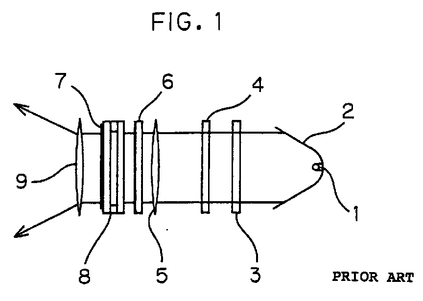
A construction of the liquid crystal projector is
shown in FIG. 1. Light generated from a light source 1
of a high luminance lamp such as a metal-halide lamp, a
xenon lamp or a UHP or the like, is reflected by a spherical
reflecting mirror 2. Then, light reflected by the
spherical reflecting mirror 2 transmits through a filter
3 so that unnecessary infrared ray and ultraviolet ray are
removed. Further, light transmitting through the filter
3 transmits through an integrator lens 4 and a condenser
lens 5 so as to be condensed, and thereafter, passes through
an incidence side polarizing plate 6, and thus, is incident
upon a liquid crystal panel 8. Light emitted from the liquid
crystal panel 8 transmits through an emission side
polarizing plate 7, and thereafter, is enlarged and
projected by means of a projection lens 9, and thus, an
image is projected onto a screen or the like located ahead
of the projector.
The aforesaid structure is of a single-panel type
using a sheet of liquid crystal panel including color
filters. In addition to the above single-panel type
structure, a three-panel type structure is also known such
that light from a light source is decomposed into
decomposition lights of three primary colors of RGB, and
these decomposition lights are incident upon three liquid
crystal panels.
A construction of the liquid crystal projector having
the above three-panel type structure is shown in FIG. 2.
In FIG. 2, like reference numerals used in the case of FIG.
1 are used to designate components having the same function
as components shown in FIG. 1. In the construction shown
in FIG. 2, the following components are used; more
specifically, dichroic mirrors 10 for transmitting or
reflecting an incident light in accordance with a wavelength,
a complex prism 11 for synthesizing light, and total
reflection mirrors 12. Light, which is generated from the
light source 1 and reflected by the spherical reflecting
mirror 2, transmits through the filter 3 and the integrator
lens 4, and thereafter, is guided to the dichroic mirrors
10 after its optical path is bent by one of the total
reflection mirrors 12. Then, light from the light source
1 is decomposed into three primary color lights of red (R),
green (G) and blue (B) by means of two dichroic mirrors
10 for reflecting or transmitting light having different
wavelength band. Then, these decomposition lights are
transmitted through the liquid crystal panel 8
corresponding to each of three primary colors, and
thereafter, are synthesized by the complex prism 11, and
thus, are projected.
In these liquid crystal projectors, there is a
tendency for a projected image to be short of a brightness.
The first factor is light absorption by polarizers 6 and
7 located front and rear the liquid crystal panel 8. The
second factor is that the liquid crystal panel 8 has an
area made snail up to a size of about 1 inch in order to
miniaturize the liquid crystal projector. More
specifically, in the case where an image of the liquid
crystal panel 8 having a small area is enlarged and projected
to several tens of inches to several hundreds of inches,
there is the case where the projected image is short of
a brightness.
In order to solve these problems as described above,
high output lamps such as high-luminance metal-halide lamp,
Ultra High Pressure Mercury lamp and xenon lamp are used
as the light source 1. However, in particular, in the
presentation system, demands for further miniaturization,
high definition and high luminance are made in the market
and a higher output lamp is selected.
For this reason, in the liquid crystal projector
system, a disadvantage by a heat is a significant problem.
For example, in general, an iodine-based polarizer
is used as the polarizer constituting a liquid crystal
display section. However, the iodine-based polarizer is
not sufficient in light resistance, heat resistance and
damp and heat resistance. For this reason, in particular,
in the liquid crystal projector, a dye-based polarizer is
used because of being excellent in light resistance, a heat
resistance and a damp and heat resistance (see Unexamined
Patent Publications (Kokai) No. 9-22008 and 9-22009)
However, in particular, the incidence side polarizer
6 has light transmittance of about 40%, and absorbs most
of lights. Further, the polarizer 6 can not maintain its
characteristic when becoming a temperature of 70°C or
higher.
Moreover, the liquid crystal panel 8 itself is weak
in a heat, and its characteristic is remarkably deteriorated
when becoming a temperature of 60°C or higher.
In order to solve the above problem, in the liquid
crystal projector, the following various cooling systems
have been proposed.
Before light from the light source 1 is incident upon
the polarizer 6, a polarizing direction is aligned with
a transmission polarization axis of the polarizer 6 so as
to reduce a quantity of light absorbed into the polarizer
6.
However, in this case, since about 20% of light
incident upon the polarizer 6 is absorbed by the polarizer
6, there is the case where a sufficient cooling effect is
not always obtained. More specifically, for example, the
liquid crystal panel 8 is made into a small size, and the
lamp intensity per unit area becomes higher, and thereby,
there is the case where a sufficient cooling effect is not
obtained.
As seen from the above description, even if the
aforesaid conventional cooling systems are employed, a
sufficient cooling effect can not be obtained with a simple
structure.
The problem of generating a heat raises in various
portions other than the polarizer 6.
For example, a pixel electrode and a switching element
are formed on an incidence side transparent substrate which
is a constituent element of the liquid crystal panel 8.
At present, the transparent substrate is constructed with
the use of a silica glass substrate having a low heat
conductivity of about 1 or 2 W/m·K. For this reason, it
is impossible to effectively release a heat accumulated
in the liquid crystal panel 8.
Recently, a panel size is made small, and thereby,
light quantity per unit area increases. In addition, in
order to improve an aperture ratio, a micro lens is used
so that an incident light is condensed and transmitted for
each pixel. Thus, as seen from the above explanation, a
thermal load acting on the liquid crystal panel itself
becomes greater.
In a driving circuit, its operating speed is slow
because in a liquid crystal display unit using a polysilicon
thin-film transistor as conventionally, a mobility of
polysilicon is slow. In addition, since a leakage current
is large due to a fault of polysilicon, there is a problem
that power consumption is much.
On the other hand, in the liquid crystal projector
having the construction as shown in FIG. 2, the dichroic
mirrors 10 are used. The dichroic mirrors 10 are
manufactured in a manner of coating a thin film, which
selects a wavelength of the light and carries out
transmission/reflection, on the surface of a blue sheet
glass or white sheet glass. The dichroic mirrors 10 also
cause a heat generation by light absorption and, therefore,
the temperature of apparatus rises up as a whole.
Moreover, there is the case where an infrared ray is
previously cut from light incident upon an optical system
from the light source 1 so as to restrict a heat generation.
The blue sheet glass or white sheet glass is used as the
filter 3 (see FIG. 2) for cutting an infrared ray. Since
these sheet glasses have low heat conductivity, a heat is
accumulated. As a result, this is a factor of a temperature
rise in the whole of apparatus.
Meanwhile, since the single light source 1 is used,
the integrator lens 4 is used in order to diffuse a light
source intensity and make uniform illuminance of an
irradiation surface. In general, the integrator lens 4
has the following structure; more specifically, an optical
glass such as Pyrex glass is subjected to mold pressing,
and many lenses thus manufactured are made into a single
plate. Further, in order to improve a characteristic,
there is the case where a material such as silica glass
is used, and a total reflection of the side plane of a prism
made of silica glass is utilized. In this case, the silica
glass has a low refractive index of about 1.46 and, therefore,
the total reflection angle becomes large. As a result,
a length of the prism rod must be set longer. Moreover,
there is a problem that the number of pseudo light sources
is small.
SUMMARY OF THE INVENTION
It is, therefore, an object of the present invention
to provide a liquid crystal display apparatus which includes
a simple and effective cooling structure.
Another object of the present invention is to provide
a projection type liquid crystal display apparatus (liquid
crystal projector) which includes a simple and effective
cooling structure.
Still another object of the present invention is to
provide a liquid crystal display apparatus which has a fast
operating speed, low power consumption and excellent
radiation property, and is adaptable to miniaturization
and high definition.
The present invention provides a liquid crystal
display device, which includes a liquid crystal panel as
one of optical components for transmitting, absorbing or
reflecting light, any one of the optical components being
comprised of a sapphire substrate.
According to one embodiment of the present invention,
the liquid crystal display device further includes a light
source, and the optical components transmits and projects
light from the light source, thereby constructing a
projection type display device.
More specifically, the optical components may further
include a lens, and a polarizer having a polarizer film
and a retaining plate for retaining the polarizer film,
and the liquid crystal panel includes a transparent
substrate, and further, any one of the lens, the retaining
plate and the transparent substrate is comprised of a
sapphire substrate, and thus, light from the light source
may be transmitted through the lens, the polarizer and the
liquid crystal panel so as to be projected.
Further, the optical components may further include
a wavelength selective optical component for transmitting
or reflecting light having a specific wavelength band, a
lens, and a polarizer having a polarizer film and a retaining
plate for retaining the polarizer film, and the liquid
crystal panel includes a transparent substrate. Any one
of the wavelength selective optical component, the lens,
the retaining plate and the transparent substrate may be
comprised of a sapphire substrate, and light from the light
source may be transmitted through the lens, the polarizer
and the liquid crystal panel so as to be projected.
In this case, the wavelength selective optical
component may be a filter (for example, an infrared cut
filter or an ultraviolet ray cut filter).
Moreover, the wavelength selective optical component
may be a dichroic mirror.
With the above construction, the sapphire substrate
having a high heat conductivity is used as a transparent
substrate in the liquid crystal projector, and thereby,
a heat radiating effect can be enhanced. More specifically,
sapphire, which is excellent in heat conductivity, is used
as various components of the liquid crystal display device,
and thereby, a heat radiating effect can be improved.
Therefore, it is possible to realize a high-luminance and
small-size liquid crystal projector without causing a
problem of characteristic deterioration by a heat
generation.
Further, a metallic radiation fin may be bonded to
the sapphire substrate, and thereby, a heat radiating effect
can be improved more.
The transparent substrate of the liquid crystal panel
may perform a function as the retaining plate of the
polarizer film. More specifically, the polarizer film may
be supported onto the surface of the transparent substrate
of the liquid crystal panel.
Preferably, the sapphire substrate is constructed in
a manner that an angle made by a C-axis direction or C-axis
projection line direction and a polarized light
transmission axis is set within a range of ±2°, or an angle
made by an axis perpendicular to the C-axis and a polarized
light transmission axis is set within a range of ±2°, or
an angle made by a C-plane and a plane vertical to a
transmission direction of a polarized light to be
transmitted is set within a range of ±2°.
Whereby it is possible to prevent an influence to
polarizing characteristic.
The lens may be an rod-type integrator lens for
diffusing light from the light source, and the integrator
lens may be formed of sapphire. More specifically, the
sapphire has a high refractive index, so that it is possible
to make small a total reflection angle, and to improve a
diffusion of light from the light source.
A transparent adhesive agent having a Shore hardness
of 30 or less may be applied onto the polarizer film or
the liquid crystal panel so as to form a thickness of 10
to 70 µm, and then, the sapphire substrate may be aligned
and banded thereto. Whereby it is possible to prevent a
deformation of the liquid crystal panel generated by a
difference of thermal expansion, and thereby, to reduce
an influence to an image while preventing a failure in a
heat conductivity
The sapphire substrate may be attached onto an outer
surface of the liquid crystal panel so as to be sealed with
a space of 0.1 mm or less interposed therebetween. Whereby
the sapphire has no influence to the liquid crystal panel,
and a generated heat is effectively conducted via a micro
space, and thus, a cooling effect can be enhanced.
Further, in the case of attaching the sapphire
substrate is attached onto an outer surface of the liquid
crystal panel, preferably, light shielding layer having
a window of a size larger by 0.1 mm or more than an effective
pixel area of the liquid crystal panel is applied to the
sapphire substrate. Whereby it is possible to prevent a
projected image from receiving an influence of scattering
light from the surroundings.
The liquid crystal panel may include a first
transparent substrate and a second transparent substrate
facing each other with a liquid crystal layer sandwiched
therebetween. In this case, it is preferable that at least
one of the first transparent substrate and the second
transparent substrate is comprised of a sapphire substrate.
Further, the liquid crystal panel may include a first
sapphire substrate and a second sapphire substrate used
as a pair of transparent substrates facing each other with
a liquid crystal layer sandwiched therebetween.
In this case, preferably, the first sapphire substrate
whose primary plane is any one of an R-plane, an A-plane,
an M-plane and a C-plane, and the second sapphire substrate
whose primary plane is any one of an R-plane, an A-plane,
an M-plane and a C-plane. Further, preferably, the first
sapphire substrate and the second sapphire substrate face
each other so that each specific crystal axis of them
substantially coincide with a polarization transmission
axis of polarized light to be transmitted.
In this case, preferably, the liquid crystal panel
further includes pixels which are arranged in a matrix on
the first sapphire substrate so as to be aligned with a
specific crystal axis direction of the first sapphire
substrate, a vertical scanning circuit and a horizontal
scanning circuit which are formed with the use of a thin
film transistor comprised of silicon made by epitaxial
growth on the first sapphire substrate, and send a video
signal to the pixels, and a transparent electrode formed
on the second sapphire substrate.
Preferably, the pixels are arranged in a matrix so
as to be substantially parallel with or perpendicular to
the specific crystal axis direction of the first sapphire
substrate.
Preferably, the first and second sapphire substrates
are constructed in a manner that an angle made by each
specific crystal axis of them and a polarization
transmission axis of a polarized light to be transmitted
is set within a range of ±2°.
Each specific crystal axis of the first and second
sapphire substrates may be an A-axis or C-axis projection
line direction in the case where its primary plane is an
R-plane, may be a C-axis or M-axis direction in the case
where its primary plane is an A-plane, may be C-axis or
A-axis direction in the case where its primary plane is
an M-plane, and may be an A-axis or M-axis direction in
the case where its primary plane is a C-plane.
The liquid crystal panel has a structure in which the
polarizers are arranged on both sides of the panel so that
their polarizing directions cross at right angle, and a
liquid crystal layer is interposed between the polarizers.
When an electric field is an on state, a liquid crystal
stands up. In the case where the electric field is an off
state, on the other hand, the liquid crystal is twisted.
By making use of this charcteristic, the liquid crystal
performs a function as a switch for shielding or
transmitting light. Therefore, an image can be formed by
carrying out an on/off control of electric field for each
pixel.
The specific axis orientation of the sapphire
substrate is made coincident with an arrangement direction
of the pixels and the polarizing direction of the polarized
light to be transmitted, whereby it is possible to prevent
the sapphire substrate from giving an influence to a
polarizing characteristic. Whereby it is possible to
realize a high-luminance and small-size liquid crystal
projector which is excellent in a heat radiating effect
without causing a problem of characteristic deterioration
by a heat generation.
Moreover, the specific axis and crystal orientation
of the sapphire substrate is controlled as described above,
and thereby, it is possible to faithfully maintain a
polarizing characteristic, and to realize a liquid crystal
projector which can project an image.
Moreover, the pixels arranging on the sapphire
substrate in a matrix, and the vertical and horizontal
scanning circuits are formed of SOS (silicon on sapphire)
thin film transistors, and thus, an active matrix type
liquid crystal display device is constructed, thereby
making it possible to increase an operating speed and to
reduce a power consumption. In addition, since an ordinary
semiconductor process can be employed, mass production is
possible and, therefore, it is possible to realize a liquid
crystal display device having various effects.
In the above embodiments, it is preferable that
antireflection coating is subjected onto a surface of the
sapphire substrate. Whereby it is possible to improve the
transmittance.
The above and further objects, features and effects
of the invention will becomes apparent from the following
detailed description with reference to the accompanying
drawings.
BRIEF DESCRIPTION OF THE DRAWINGS
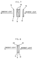
FIG. 1 is a view schematically showing a construction
of a transmission liquid crystal single-panel type
projector;
FIG. 2 is a view schematically showing a construction
of a transmission liquid crystal three-panel type
projector;
FIG. 3 is a view showing a construction of a polarizer
used in a liquid crystal projector according to one
embodiment of the present invention;
FIG. 4 is a view showing a construction of a polarizer
used in a liquid crystal projector according to another
embodiment of the present invention;
FIG. 5 is a view showing a liquid crystal panel
including the polarizer shown in FIG. 3 or FIG. 4;
FIG. 6 is a view shoving a liquid crystal panel
including the polarizer shown in FIG. 3 or FIG. 4;
FIG. 7 is a view showing a liquid crystal panel
according to still another embodiment of the present
invention;
FIG. 8 is a view showing a liquid crystal panel
according to still another embodiment of the present
invention;
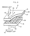
FIG. 9 is an exploded perspective view showing a
construction of a liquid crystal display device according
to still another embodiment of the present invention;
FIG. 10 is a view showing a circuit configuration of
the liquid crystal display device according to still another
embodiment of the present invention;
FIG. 11 is a cross sectional view schematically
showing a unit pixel and a SOSMOS transistor switching
section of the liquid crystal display device shown in FIG.
10;
FIG. 12 is a view showing a liquid crystal panel
according to still another embodiment of the present
invention;
FIG. 13 is a view showing a liquid crystal panel
according to still another embodiment of the present
invention;
FIG. 14 is a view showing still another embodiment
of the present invention; and
FIG. 15 is a view showing a crystal structure of
sapphire.
DESCRIPTION OF THE PREFERRRED EMBODIMENT
According to one embodiment of the present invention,
in the liquid crystal projector having the construction
shown in FIG. 1 or FIG. 2, at least one of the optical
components is formed of a sapphire substrate. The optical
components include: dichroic mirrors 10; a filter 3; a lens
4; a retaining plate of a polarizer film (material) in the
polarizer 6,7; and a transparent substrate constituting
the liquid crystal panel 8. A sapphire substrate has high
heat conductivity, so that a heat generated from the optical
components can be effectively radiated.
First, the following is a description on an embodiment
using a sapphire substrate as the retaining plate of the
polarizer 6,7.
As shown in FIG. 3, the polarizer 6,7 is manufactured
in a manner of bonding a polarizer film 13 to a surface
of a retaining plate 15 comprised of a sapphire substrate
by means of a sheet-like transparent bonding agent
interposed therebetween. In this case, the polarizer film
13 and the retaining plate 15 are bonded together so that
an angle made by a transmission polarizing axis 14 of the
polarizer film 13 and an axis 16 is set within a range of
±2°, preferably, ±0.5°. The axis 16 is a C-axis of the
sapphire substrate constituting the retaining plate 15 or
an axis indicating a C-axis projection line direction or
an axis (e.g., M-axis) perpendicular to the C-axis. This
serves to prevent a polarized light shaped by the polarizer
film 13 from generating an optical rotation resulting from
a birefringence or double refraction in a sapphire crystal.
In the case where the angle made by the two axes is set
more than the above angular range, any influence such as
disturbance appears in an image projected from the liquid
crystal projector.
Moreover, as shown in FIG. 4, a surface orientation
of a primary plane 15a of the retaining plate 15 comprised
of the sapphire substrate is set within a range of C-plane
±2°, preferably, ±0.5°. Whereby a stable image can be
obtained without receiving an influence by double
refraction.
FIG. 5 shows a state that the polarizers 6 and 7 aligned
as shown in FIG. 3 are set front and rear the liquid crystal
panel 8, and light is irradiated thereto. In this case,
the incidence side polarizer 6 is arranged separating from
the liquid crystal panel 8 with a distance of 1 to 5 mm.
On the other hand, the emission side polarizer 7 is directly
applied to the liquid crystal panel 8 by means of a sheet-like
transparent bonding agent in a state that the polarizer
film 13 faces the surface of the liquid crystal panel 8.
The polarizers 6 and 7 are constructed in a manner
of applying the polarizer films 13 to the retaining plates
15 comprised of sapphire substrates having a high heat
conductivity of 42 W/m·K. Thus, a heat accumulated by
absorption of light incapable of transmitting through the
polarizer film 13, is conducted to the sapphire substrate,
so that the heat can be effectively radiated. These
polarizers are used in combination with a cooling fan, and
thereby, a heat of the polarizers 6 and 7 can be effectively
radiated.
In order to obtain the best display contrast of the
liquid crystal panel 8, in the polarizer 6, it is preferable
that the polarizer film 13 applied onto the retaining plate
15 is arranged on the liquid crystal panel 8 side so as
to face the panel 8. Moreover, in the polarizer 7, it is
preferable that the polarizer film 13 applied onto the
retaining plate 15 is arranged on the liquid crystal panel
8 side so as to face the panel 8.
The reason is because it is significant that change
in a polarizing characteristic of light before and after
transmitting through the liquid crystal panel 8 is made
as little as possible. Even if the retaining plate 15 made
of sapphire is accurately set in its crystal axis
orientation and crystal orientation, light transmitting
through the retaining plate 15 receives some changes in
its polarizing characteristic. Therefore, the polarizer
film 13 is arranged on the liquid crystal 8 side, and thereby,
it is possible to realize a contrast characteristic of the
same level as the case of using no sapphire substrate (e.g.,
the case of using a glass substrate).
As shown in FIG. 6, the incidence side polarizer 6
may be applied directly onto the surface of the liquid
crystal panel 8. In this case, the sapphire substrate
having preferable heat conductivity is used as the retaining
plate 15, and thereby, a sufficient heat radiating effect
can be obtained. In this structure, a cooling air does
not reach the surface of the liquid crystal panel 8 and,
therefore, no dust adheres to the surface. A dust may adhere
to the surface of the retaining plate 15. However, the
surface of the retaining plate 15 diverges from a focal
plane of a projection optical system, so that an image of
the dust is not vividly imaged on a projection screen. As
a result, by the structure as shown in FIG. 6, it is possible
to prevent a deterioration of quality of the projected
image.
Preferably, the sapphire substrate used as the
retaining plate 15 is subjected to antireflection coat at
its one side or both sides so as to improve its transmitivity.
In this case, it is preferable that in the antireflection
coat, coating characteristic is made different between a
bonding surface with the polarizer film and a surface
contacting with an air, so as to meet a refractive index
of a contacting layer (polarizer film 13 or air). This
further improves the transmitivity.
For example, a surface of the sapphire substrate
(retaining plate 15) contacting with an air may be subjected
to antireflection coat with respect to the refractive index
of about 1.0. In this case, it is preferable that the
antireflection coating has a refractive index within a range
of 1.3 ± 0.15. To give an example, MgF2 having a refractive
index of 1.38 is applicable as the antireflection coat.
Moreover, preferably, a bonding surface with another member
(polarizer film 13) is subjected to antireflection coat
with respect to a refractive index of 1.38 to 1.55 so as
to meet a transparent adhesive agent which will be described
later.
It is preferable to provide a frame-like light
shielding film on a sapphire substrate used as the polarizer
7 arranged on the emission side of the liquid crystal panel
8. The light shielding film has a window. Preferably, the
window has a size which is 0.1 mm or more larger than an
effective pixel area of the liquid crystal panel 8, and
has a transmittance of 1% or less. Whereby it has been
confirmed that it is possible to solve the problem that
a contrast of a projected image lowers due to an influence
of a scattering light from the surrounding. The light
shielding film may be formed by silk screen printing, or
may be formed of a chrome-based deposition film.
In fact, in the case where the polarizers 6 and 7 are
constructed with the use of the sapphire substrate as the
retaining plate 15, these polarizers 6 and 7 individually
have an improvement of 10 to 15°C or more in their cooling
effect as compared with the conventional case of using the
blue sheet glass or white sheet glass as the retaining plate.
Next, the following is a description on an embodiment
of using a sapphire substrate as a transparent substrate
constituting the liquid crystal panel 8.
The liquid crystal panel 8 has a structure in which
a liquid crystal is held between an incidence side
transparent substrate and an emission side transparent
substrate. Pixel electrodes and switching elements are
formed on the incidence side transparent substrate. Facing
electrodes are formed on the emission side transparent
substrate. Thus, the incidence side and/or emission side
substrate is composed of a sapphire substrate. Or, apart
from the transparent substrate of the liquid crystal panel
8, a transparent substrate comprised of the sapphire
substrate may be provided on the incidence side and/or
emission side substrate of the liquid crystal panel 8.
FIG. 7 shows an embodiment of providing transparent
substrates 18 comprised of sapphire substrates on the
incidence side and emission side of the liquid crystal panel
8 apart from the liquid crystal panel 8. The transparent
substrate 18 is bonded to the liquid crystal panel 8 in
a state of forming a space of 0.1 mm or less between the
outer surface of the transparent substrate of the liquid
crystal panel 8 and the transparent substrate 18, and
closing the formed space.
In the liquid crystal panel 8 used in the liquid crystal
projector, no beads is encapsulated in a liquid crystal
layer in order to keep the space constant. Because, if
the beads were encapsulated in the space, a quality of an
enlarged and projected image would be lost. Therefore,
in a pair of transparent substrates constituting the liquid
crystal panel 8, a mutual interval is kept by only seal
layer of an outer peripheral portion surrounding the liquid
crystal layer. In the case where the sapphire transparent
substrate is mounted to the outer surface of the liquid
crystal panel 8 in a state of contacting therewith, the
surface of the liquid crystal panel 8 is deformed by a thermal
expansion due to a temperature change. For this reason,
ununiformity is generated in the liquid crystal layer. As
a result, a quality of a projected image is worsened.
So, in this embodiment, the transparent substrate 18
are arranged with spaces from the surfaces of the liquid
crystal panel 8. On the other hand, in order to effectively
conduct an accumulated heat of the liquid crystal panel
8 to the transparent substrates 18, it is preferable to
make narrow spaces between the liquid crystal panel 8 and
the transparent substrates 18 as much as possible. The
space may be set to 0.1 mm or less, and thereby, it is possible
to prevent a surface deformation of the liquid crystal panel
8, while securing a heat radiating effect.
Moreover, in this embodiment, the
transparent
substrates 18 have been bonded to the
liquid crystal panel
8 with the closed spaces sandwiched therebetween. In place
of the spaces, the
transparent substrates 18 may be stuck
onto the surfaces of the
liquid crystal panel 8 with a
sheet-like transparent adhesive agent or bonding agent
interposed therebetween that has a flexibility. In this
case, as shown in the Table 1, the transparent adhesive
agent having a Shore hardness of 30 or less may be used,
and thereby, it is possible to preferably secure an image
quality. Moreover, in the case of taking an influence to
the image quality into consideration, if a thickness of
the transparent adhesive agent is set to 10 µm or more,
there is no problem. An experiment was conducted in order
to confirm a cooling performance by heat conduction. As
a result, as shown in the Table 2, it can be seen that a
preferable cooling effect is obtained if the thickness of
the transparent adhesive agent is set to 70 µm or less.
| Adhesive agent hardness (Shore hardness) | Image quality (including bond quality) |
| 10 | ○ |
| 20 | ○ |
| 30 | ▵ |
| 40 | X |
| 50 | X |
| 60 | X |
| Thickness of adhesive layer (mm) | Image quality (including bond quality) | Cooling effect |
| 5 | X | ○ |
| 10 | ▵ | ○ |
| 15 | ○ | ○ |
| 20 | ○ | ○ |
| 30 | ○ | ○ |
| 40 | ○ | ○ |
| 50 | ○ | ○ |
| 60 | ○ | ○ |
| 70 | ○ | ▵ |
| 80 | ○ | ▵ |
| 90 | ○ | ▵ |
| 100 | ○ | ▵ |
| 110 | ○ | X |
| 120 | ○ | X |
In Table 1 and Table 2, a symbolic mark "○" is given
in the case where a preferable result is obtained, a symbolic
mark "▵" is given in the case where the result within a
allowable limit range is obtained, and a symbolic mark "X"
is given in the case where the result not being allowable
is obtained.
The transparent substrates 18 are arranged on both
incidence side and emission side of the liquid crystal panel
8, and thereby, a higher heat radiating effect can be
realized. It is possible to obtain a high heat radiating
effect even if the transparent substrate is arranged on
only one side. Moreover, an antireflection coat may be
subjected to one surface or both surfaces of the sapphire
substrates constituting the transparent substrates 18, and
thereby, it is possible to improve a transmission
characteristic.
In the sapphire substrates constituting the
transparent substrates 18, an angle made by a C-axis of
the sapphire substrate or a C-axis projection line or an
axis perpendicular to the C-axis is set within a range of
±2°, preferably ±0.5°, with respect to a polarization axis
of a polarized light to be transmitted. Whereby it is
possible to prevent a deterioration of a projected image
quality due to light rotation. In addition, a surface
orientation of the sapphire substrate may be set within
a range of ±2°, preferably ±0.5°, with respect to the
C-surface, and thereby, it is possible to prevent from
giving an influence to the projected image quality.
Further, in this embodiment, the surface of the liquid
crystal panel 8 is covered with heat radiating plates
comprised of the sapphire transparent substrates 18. Even
if a dust adheres to the transparent substrates 18, no
hindrance is generated in an image quality. Because a focal
plane of a projection optical system is aligned with the
liquid crystal panel 8, and the surface of the transparent
substrate 18 diverges from the focal plane. According to
the experiment, a distance of 1 mm or more was required
between the liquid crystal panel 8 and the surface of the
transparent substrate 18 (the surface opposite to the liquid
crystal panel 8).
In addition, with the use of the retaining plates 15
constituting the polarizers 6 and 7 composed of the sapphire
substrate, the following effect was obtained; more
specifically, a liquid crystal panel surface temperature
lowered about 5°C or more.
FIG. 8 shows an embodiment in which an incidence side
transparent substrate 19 and an emission side transparent
substrate 20 constituting a transmission type liquid
crystal panel 8 are composed of sapphire substrates.
In first and second sapphire substrates 19 and 20,
the following construction is required; more specifically,
an angle made by a polarization axis of a polarized light
to be transmitted and an axis is set within a range of ±2°,
preferably ±0.5°. The axis is a C-axis of a crystal axis
of sapphire substrate or a C-axis projection line or an
axis perpendicular to the C-axis. Alternatively, a surface
orientation of the sapphire substrate may be set within
a range of ±2°, preferably ±0.5°.
In this construction, the transparent substrates 19
and 20 constituting a transmission type liquid crystal panel
8 are composed of sapphire substrates having a sufficient
heat radiating effect. Thus, there is no need of
specifically providing the polarizing plate, because the
polarizer film 13 may be bonded directly to each outer
surface side of the transparent substrates 19 and 20. By
doing so, the transparent substrates 19 and 20 also
functions as a retaining plate of the polarizer film 13.
Therefore, it is possible to provide a compact structure
at a low cost.
In this case, an antireflection coat may be subjected
to one surface or both surfaces of the sapphire substrate,
and thereby, it is possible to further improve a
transmission characteristic. However, in general, the
transparent adhesive agent for bonding the polarizer film
13 has a refractive index of 1.4 to 1.5, and also, performs
a function of partially antireflection. Thus, even if no
antireflection coating is subjected in particular, it is
possible to realize a preferable transmission
characteristic. Of course, antireflection coating may be
subjected to the sapphire substrates according to a
refractive index of the transparent adhesive agent, and
thereby, the transmission characteristic can be further
improved.
In the structure shown in FIG. 8, in the case where
a cooling structure combining a cooling fan is employed,
it is possible to realize a temperature reduction effect
of about 15 to 20°C and a temperature distribution uniformity
as compared with the case of forming the same structure
as above with the use of quartz substrates. Further, an
optical path of an optical system can be shortened about
5%.
FIG. 9 shows a structure of a liquid crystal panel
8 according to another embodiment. In FIG. 9, like
reference numerals are used to designate portions
corresponding to the components shown in FIG. 8.
The first sapphire substrate 19 is formed with pixels
36, in a anatrix pattern on its inside surface, each
including a pixel electrode and switching element, and the
polarizer film 13 is stuck on to the outer side of the sapphire
substrate 19 so as to be aligned with the matrix pattern.
Moreover, the second sapphire substrate 20 facing the first
sapphire substrate 19 is formed with a transparent facing
electrode 37, and another polarizer film 13 is stuck onto
the outer side of the sapphire substrate 20. The
polarization axis directions of the two polarizer films
13 are parpendicular to each other. A liquid crystal is
encapsulated between the first and second sapphire
substrates 19 and 20 faced in the aforesaid manner, and
thus, the liquid crystal panel is formed.
It is assumed that a polarized light 40 shaped into
a polarization direction 38 is incident from the outside
of first sapphire substrate 19. A liquid crystal
vertically stands in a pixel whose electric field is in
an on state and, therefore, the polarized light 40 straight
advances through the pixel with the polarization direction
remain unchanged. The polarized light 40 is therefore
absorbed by the emission side polarizer film 13, and then,
the pixel becomes a black indication. In a pixel whose
electric field is in an off state, since the liquid crystal
becomes in a twisted state, the polarized light 40 is rotated
by an angle of 90° in its polarization direction, and then,
has a polarization direction 39. Thus, the polarized light
40 passes through the emission side polarizer film 13, so
that the pixel becomes an operating or lighting state.
In the first and second sapphire substrates 19 and
20, one of R-plane, A-plane, M-plane and C-plane is used
as a primary plane. A specific crystal axis direction of
each of sapphire substrates 19 and 20, is substantially
coincident with an arrangement direction of the pixels 36
and a polarization axis direction of polarized light to
be transmitted. In this case, the above specific crystal
axis direction is an A axis or C axis projection line
direction in the case where the primary plane is the R-plane,
is a C-axis or M-axis direction in the case where the primary
plane is the A-plane, is a C-axis or A-axis direction in
the case where the primary plane is the M-plane, and is
an A-axis or M-axis direction in the case where the primary
plane is an M-plane.
More specifically, the specific crystal axis
direction of the first sapphire substrate 19 and the
arrangement direction of the pixels 36 are set substantially
parallel or perpendicular, and an angle made by the specific
crystal axis direction of the first sapphire substrates
19 and 20 and the polarization axis direction of polarized
light to be transmitted is set within a range of ±2°,
preferably ±0.5°. In the first and second sapphire
substrates 19 and 20, since a direction of the polarized
light to be transmitted is different, these sapphire
substrates 19 and 20 are arranged, accordingly.
This arrangement ensures that a polarized light shaped
by the polarizer film 13 does not generate light rotation
resulting from a birefringence in sapphire crystal. For
example, in the case where an angle exceeds the aforesaid
angular range, an influence such as disturbance is caused
in an image projected from the projector.
Moreover, in the case where the primary plane of the
sapphire substrates 19 and 20 is the R-plane, a silicon
film can be formed on the surface by epitaxial growth, and
thereby, the silicon film becomes a single crystal (SOS
= Si ON SAPPHIRE). Therefore, it is possible to obtain
an effect such that a thin-film transistor characteristic
using the silicon film is greatly improved. Whereby a
display speed can be greatly improved, and also, a power
consumption can be reduced.
The first and second sapphire substrates 19 and 20
constituting the liquid crystal panel 8 has a sufficient
heat radiating property or effect. Thus, there is no need
of specially providing a polarizing plate, and the polarizer
films 13 may be bonded directly to the outer surfaces of
the first and second sapphire substrates 19 and 20. By
doing so, these first and second sapphire substrates 19
and 20 can be also used as the retaining plates of the
polarizer films 13, thereby making it possible to make
compact an optical path, and to provide a low cost structure.
In addition, by employing a structure in which the
polarizer film 13 is separated from the liquid crystal panel,
a more sufficiently cooling effect can be obtained. The
first and second sapphire substrates 19 and 20 may be set
to a thickness of 2 mm or more, and thereby, it is possible
to improve a deterioration of image quality due to a dust
adhered to the panel surface by means of a defocus effect.
Next, FIG. 10 shows a circuit configuration of a liquid
crystal panel in the case of using the first sapphire
substrate 19 whose primary plane is an R-plane. As shown
in FIG. 10, pixels 41 are arranged like a matrix on the
first sapphire substrate 19. Each pixel 41 is provided
with a SOSMOS transistor switch 42 which is formed of a
single crystal silicon by epitaxial growth on the sapphire
substrate 19. Further, the first sapphire substrate 19
is formed with a vertical scanning circuit 43 for driving
a gate of the SOSMOS transistor switches 42, and a horizontal
scanning circuit 44 for transferring a video signal to each
signal line 45 in order. Also, MOS transistors required
for these vertical scanning circuit 43 and horizontal
scanning circuit 44 are formed of SOSMOS transistors.
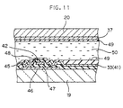
FIG. 11 shows a schematically cross section of the
unit pixel 41 and the SOSMOS transistor switch 42 in the
liquid crystal display device.
A single crystal silicon layer 46 is formed on the
primary plane of the first sapphire substrate 1 by epitaxial
growth so that a crystal orientation of the primary plane
becomes an R-plane, and then, impurities are doped in the
formed single crystal silicon layer so as to form a thin
film transistor. Further, a gate 48 insulated by a SiO2
layer 47 is formed on the thin film transistor, and thus,
a SOSMOS transistor 42 is formed as a whole.
One end of the SOSMOS transistor switch 42 is connected
to the signal line 45 to which the video signal from the
horizontal scanning circuit 44 is transferred. Another
end of the SOSMOS transistor switch 42 is connected to a
transparent electrode 33 (pixel 41) formed of an ITO and
the like, and thus, a pixel 41 is constituted. Further,
a transparent electrode 37 is formed on the sapphire
substrate 20 facing the sapphire substrate 19 on which the
pixels 41 and SOSMOS transistor switches 42 are formed,
and liquid crystal alignment layers 49 are interposed so
that a liquid crystal 50 is held between these alignment
layers.
Then, when the gate of each SOSMOS transistor switch
42 is driven by means of the vertical scanning circuit 43,
a video signal flows through the transparent electrode 33
(pixel 41) from the signal line 45, and thus, the pixel
41 is operated.
Although not illustrated, MOS transistors used in the
horizontal scanning circuit 44 and the vertical scanning
circuit 43 are also comprised of SOSMOS transistor switches.
More specifically, in the same manner as described above,
the MOS transistors are comprised of thin film transistors
which are formed of a single crystal silicon formed by
epitaxial growth on the sapphire substrate 19.
In the liquid crystal display device of this
embodiment, the single
crystal silicon layer 46 is used
for forming thin film transistors. The single
crystal
silicon layer 46 has almost no defect and, therefore, a
leakage current is small, and a power consumption can be
reduced. Further, since the single
crystal silicon layer
46 has a high current response, it is possible to make high
an operating speed, and to prevent a pixel shift in a
displayed image. For example, in comparison with a
mobility of electron, as shown in Table 3, a single crystal
silicon shows a mobility of about three times as much as
polysilicon.
| | | Electron mobility (cm2/V.sec) |
| Present Invention | SOS single crystal silicon film | 300∼400 |
| Comparative Example | Polysilicon | | 40∼150 |
In addition, the liquid crystal display device of this
embodiment can be readily manufactured by a conventional
C-MOS process technology of single crystal silicon because
the sapphire substrate 19 is used. Further, because the
sapphire substrate is usable in a high temperature process
of 1000°C or more, production line of a semiconductor may
be employed.
The above embodiment has described the process and
structure in which a single crystal silicon film is formed,
and thus, a liquid crystal panel is manufactured. The
sapphire substrate is applicable to a high temperature
process of a polycrystal silicon (p-Si) TFT manufacturing
process without problems, and therefore, a liquid crystal
panel can be manufactured without problems.
FIG. 12 shows an embodiment in the case where the
present invention is applied to a reflection type liquid
crystal panel 8. In this case, the liquid crystal panel
8 is constructed in a manner that a liquid crystal is
encapsulated between a transparent substrate 21 on which
reflective electrodes and switching elements are formed,
and an incidence/emission side transparent substrate 22
on which a facing electrode is formed. Sapphire substrates
are used as these transparent substrates 21 and 22. This
construction can also improve a heat radiating effect.
Since the sapphire substrate used as the transparent
substrate 21 has no influence to a polarized light
characteristic, its axis and crystal orientation may be
arbitrary. Only reflective surface side of the transparent
substrate may be subjected to mirror polishing. A
radiation heat sink 23 may be attached directly to the back
side of the transparent substrate 21. On the other hand,
in the sapphire substrate used as the incidence/emission
side transparent substrate 22, since an incident light and
a reflected emissive light are different in a polarizing
direction, the primary plane is set within C-plane ±2°,
preferably, ±0.5° so that no light rotation is generated
with respect to a polarized light.
Another embodiment of the present invention will be
described below.
In the case where a high definition image display is
required, the projector for enlarging and projecting an
image employs the following system regardless of being any
of a transmission liquid crystal type, a reflective liquid
crystal type and a DLP type. More specifically, as shown
in FIG. 2, the light source color is separated into three
color lights of RGB, and an image corresponding to each
color of RGB is displayed, and further, is synthesized by
using a prism or the like.
In this case, the dichroic mirrors 10, which perform
a function separating a color of the light source 1, are
formed of sapphire substrates, and then, the surface of
each of the sapphire substrate is formed with a film which
selects a wavelength of the light source 1, and carries
out transmission/reflection.
Whereby it is possible to effectively radiate a heat
accumulated in dichroic mirrors 10, and thus, to reduce
a temperature of the whole system. In the sapphire
substrates used as described above, a C axis or the C-axis
projection line direction or an axis perpendicular to the
C axis is set within ±2°, preferably, ±0.5° with respect
to a polarizing transmission axis adjusted after or before
transmission. Or the primary plane of the sapphire
substrate is set within a C-plane ±2°, preferably, ±0.5°.
In still another embodiment, a sapphire substrate is
used in an infrared ray cut filter 3 for preventing an
infrared ray from the light source 1 of unnecessary heating
factor from being incident upon an optical system, and an
infrared cut film may be formed on the surface of the sapphire
substrate. In this case, since the filter 3 is arranged
just after the light source 1 which is cooled by using a
cooling fan, it is possible to effectively improve a heat
radiating effect by cooling the filter 3 by means of the
cooling fan. As a result, a temperature reduction effect
of the whole system can be greatly improved.
In the sapphire substrate used as described above,
a C axis or the C axis projection line direction or a direction
perpendicular to the C axis is set within ±2°, preferably,
±0.5° with respect to a polarizing transmission axis
adjusted after or before transmission. Or the primary
plane of the sapphire substrate is set within a C-plane
±2°, preferably, ±0.5°.
A metallic radiation fin may be bonded to the above
sapphire substrate. For example, as shown in FIG. 13,
metallized layers 24 such as of Mo-Mn is formed on outer
peripheries of the sapphire substrates used as the retaining
plates of the polarizers 6 and 7, and then, metallic
radiation fins 25 are brazed thereto.
In this case, a heat accumulated in the polarizer film
13 is conducted to the retaining plate 15 made of sapphire,
and further, is effectively conducted to the metallic
radiation fin 25 having a high heat conductivity. Then,
a surface area of the metallic radiation fin 25 is made
large so as to improve a heat radiating effect, and the
radiation fin 25 may be cooled by a cooling fan, and thereby,
a cooling effect can be further improved.
According to an experiment, a temperature reduction
effect of 5 to 10°C was improved as compared with the case
that only sapphire substrates were used. Whereby it is
possible to satisfy a stable operating condition further
lower than 70°C which is a characteristic guarantee
temperature of the polarizer film 13.
In this embodiment, Mo-Mn metallization method has
been employed. In the case of manufacturing the metallic
radiation fin by employing an active metalizing method,
the same effect can be also obtained.
A general resin frame (mold) used for positioning an
optical system may be replaced by one formed of a material
such as aluminum having high heat conductivity, and thereby,
a heat is effectively conducted and, as a result, the whole
system can have a heat radiating structure.
Still another embodiment of the present invention ill
be described below.
In the projector for enlarging and projecting an image,
as shown in FIG. 14, a rod type integrator lens 26 for
diffusing light from the light source 1 of high luminance
lamp is formed of sapphire.
The sapphire is a transparent material having a high
refractive index of No = 1.768. Thus, in the case where
a quadrangular prism integrator lens 26 is manufactured
with the use of sapphire, it is possible to set a total
reflection angle smaller. Therefore, it is possible to
greatly improve diffusion as compared with the case where
the integrator lens is manufactured with the use of an
optical glass such as quartz or the like. Further, it is
possible to make a design such that a dimension of the
integrator lens is made compact.
Whereby it is possible to improve a uniformity of image
luminance by the liquid crystal projector, and also, to
improve a heat radiating effect. An antireflection coat
may be applied to end faces of the quadrangular prism, which
are an incident face and an emissive face of the integrator
lens 26, and thereby, it is possible to improve a
transmission efficiency.
Next, the following is a description on a
manufacturing process of sapphire used in the present
invention.
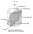
A single crystal sapphire is a single crystal of
alumina (Al2O3), and an aluminum atom and an oxygen atom
are arranged so as to form a crystal. As shown in FIG.
15, sapphire has a hexagonal system, and its center axis
is a C-axis, and a plane vertical to the C-axis is a C-plane
(0001). A plane vertical to an A-axis (a1, a2, a3) radially
extending from the C-axis is an A-plane (1120). An R-plane
exists in a state of having a predetermined angle (about
32.382°) with respect to the C-axis. These axes and planes
can be analyzed by an X-ray diffraction.
The single crystal sapphire used in the present
invention is manufactured by an EFG (Edge-defined Film-fed
Growth) method, for example. More specifically, high
purity alumina is melt in an inert atmosphere, and then,
a molybdenum die for a single crystal growth of ribbon-like
sapphire including a slit in its interior is positioned
so as to contact with the alumina molten solution. Then,
the alumina molten solution is guided to an upper end portion
of the molybdenum die by a capillary action so as to contact
with a seed crystal. Subsequently, the seed crystal is
upwardly pulled up, and then, sapphire which is a single
crystal alumina is grown. When pulling up and growing a
substrate raw material, a primary plane of the seed crystal
is set as a growth crystal orientation, and its growth axis
is set as a pull-up axis, and thus, the seed crystal is
pulled up. By pulling up the seed crystal in this manner,
it is possible to readily obtain a desired plane and crystal
axis orientation of the primary plane, and thus, to
accurately grow a single crystal sapphire.
The single crystal sapphire growth method is not
limited to the EFG method, and other methods such as a
Czochralski method may be employed. In the case of obtain
an angular-shaped crystal, the EFG method of accurately
obtaining a plate-shaped crystal is adaptable because a
cylindrical-shaped crystal has a worse efficiency.
The single crystal sapphire thus obtained is subjected
to grinding by a diamond wheel or the like so as to obtain
a desired shape, and thereafter, is subjected lapping with
the use of diamond abrasives.
Next, the single crystal sapphire and an abrasive
cloth are relatively slid while supplying a liquid in which
SiO2 colloidal ball particles having a grain size of 50
nm or less are scattered, as an abrasive slurry, and then,
CMP (Chemical Mechanical Polishing) is carried out. This
polishing process advantageously removes a fracture layer
generated by the aforesaid grinding and lapping without
newly causing a strain, so as to obtain a preferable smooth
surface which is excellent in a transmission property even
in the case of using the single crystal sapphire as a
substrate.
Next, the following Table 4 shows characteristic
values of the result of comparing the sapphire with a silica
glass, BK-7 (trade name: made of Hoya glass Co., Ltd.) and
a blue sheet glass (float glass), which are a currently
used transparent material.
| Characteristic data |
| | Sapphire | Silica glass (synthesis) | BK7 | Blue sheet glass |
| Melting point (°C) | 2053 | 1600 | 870 | 720 |
| Bending strength (MPa) | 690 | 670 | 590 | 643 |
| Young's modulus (MPa) | 4.7 × 10⁵ | 7.3 × 10⁴ | 7.2 × 10⁴ | 7.2 × 10⁴ |
| Thermal conductivity (W/m.K) | 42.0 | 1.2 | 1.0 | 0.8 |
| Vickers hardness | 2300 | 900 | 570 | 548 |
| Refractive index at 589 nm | No = 1.768 | Nd = 1.459 | Nd = 1.517 | Nd = 1.52 |
| Ne = 1.760 |
| Thermal expansion coefficient | C-axis parallel: 5.3 × 10⁻⁶/K | 0.51 × 10⁻⁶/K (0 - 100°C) | 9.8 × 10⁻⁶/K (25 - 350°C) | 8.5 × 10⁻⁶/K (25 - 350°C) |
| C-axis vertical: (25°C) 4.5 × 10⁻⁶/K |
As is apparent from the above Table 4, the sapphire
is superior in heat conductivity and is also superior in
heat radiating effect. It is also apparent that the
sapphire has a high refractive index and, therefore, a high
characteristic value can be obtained in the case where the
sapphire is used as an integrator lens.
Moreover, the sapphire has a high strength and,
therefore, it is possible to make a design of making the
sapphire thin as compared with other materials, and to make
a design of a compact optical system as a whole. In addition,
the sapphire is excellent in a heat resistance and,
therefore, the sapphire is applicable to a high temperature
process of a manufacturing process of a polycrystal silicon
(p-Si) TFT constituting a liquid crystal panel without
problem.
As this invention may be embodied in several forms
without departing from the sprit of essential
characteristics thereof, the aforesaid embodiments are
therefore illustrative and not restrictive. Since the
scope of the invention is defined by the appended claims
rather than by the description preceding them, and all
changes that fall within metes and bounds of the claims,
or equivalence of such metes and bounds thereof are
therefore intended to be embraced by the claims.
This application claims the convention priority on
the basis of Patent Application No. 11-52061 filed on March
1, 1999 with the Japanese Patent Office, and Patent
Application No. 10-371720 filed on December 28, 1998 with
the Japanese Patent Office, and the disclosure of these
applications is fully incorporated herein by reference.