EP1016107B1 - Method for producing a double layer capacitor - Google Patents
Method for producing a double layer capacitor Download PDFInfo
- Publication number
- EP1016107B1 EP1016107B1 EP98923924A EP98923924A EP1016107B1 EP 1016107 B1 EP1016107 B1 EP 1016107B1 EP 98923924 A EP98923924 A EP 98923924A EP 98923924 A EP98923924 A EP 98923924A EP 1016107 B1 EP1016107 B1 EP 1016107B1
- Authority
- EP
- European Patent Office
- Prior art keywords
- members
- flanges
- particles
- connection layer
- electrode
- Prior art date
- Legal status (The legal status is an assumption and is not a legal conclusion. Google has not performed a legal analysis and makes no representation as to the accuracy of the status listed.)
- Expired - Lifetime
Links
Images


Classifications
-
- H—ELECTRICITY
- H01—ELECTRIC ELEMENTS
- H01G—CAPACITORS; CAPACITORS, RECTIFIERS, DETECTORS, SWITCHING DEVICES, LIGHT-SENSITIVE OR TEMPERATURE-SENSITIVE DEVICES OF THE ELECTROLYTIC TYPE
- H01G4/00—Fixed capacitors; Processes of their manufacture
- H01G4/002—Details
- H01G4/228—Terminals
- H01G4/232—Terminals electrically connecting two or more layers of a stacked or rolled capacitor
-
- H—ELECTRICITY
- H01—ELECTRIC ELEMENTS
- H01G—CAPACITORS; CAPACITORS, RECTIFIERS, DETECTORS, SWITCHING DEVICES, LIGHT-SENSITIVE OR TEMPERATURE-SENSITIVE DEVICES OF THE ELECTROLYTIC TYPE
- H01G11/00—Hybrid capacitors, i.e. capacitors having different positive and negative electrodes; Electric double-layer [EDL] capacitors; Processes for the manufacture thereof or of parts thereof
- H01G11/10—Multiple hybrid or EDL capacitors, e.g. arrays or modules
- H01G11/12—Stacked hybrid or EDL capacitors
-
- H—ELECTRICITY
- H01—ELECTRIC ELEMENTS
- H01G—CAPACITORS; CAPACITORS, RECTIFIERS, DETECTORS, SWITCHING DEVICES, LIGHT-SENSITIVE OR TEMPERATURE-SENSITIVE DEVICES OF THE ELECTROLYTIC TYPE
- H01G11/00—Hybrid capacitors, i.e. capacitors having different positive and negative electrodes; Electric double-layer [EDL] capacitors; Processes for the manufacture thereof or of parts thereof
- H01G11/74—Terminals, e.g. extensions of current collectors
-
- Y—GENERAL TAGGING OF NEW TECHNOLOGICAL DEVELOPMENTS; GENERAL TAGGING OF CROSS-SECTIONAL TECHNOLOGIES SPANNING OVER SEVERAL SECTIONS OF THE IPC; TECHNICAL SUBJECTS COVERED BY FORMER USPC CROSS-REFERENCE ART COLLECTIONS [XRACs] AND DIGESTS
- Y02—TECHNOLOGIES OR APPLICATIONS FOR MITIGATION OR ADAPTATION AGAINST CLIMATE CHANGE
- Y02E—REDUCTION OF GREENHOUSE GAS [GHG] EMISSIONS, RELATED TO ENERGY GENERATION, TRANSMISSION OR DISTRIBUTION
- Y02E60/00—Enabling technologies; Technologies with a potential or indirect contribution to GHG emissions mitigation
- Y02E60/13—Energy storage using capacitors
Definitions
- the invention relates to a method for producing a double layer capacitor.
- the terminals are usually connected to the respective electrodes by "staking" or spot welding. While these operations have the advantage of simplicity and low cost they are also known to distort the shape of the electrodes and thereby compromise the quality and longevity of the capacitor. Additionally, the resultant electrical connection between the terminals and electrodes often have a high electrical resistance, thereby increasing the overall series resistance of the capacitor.
- the prior art also suffers from the limitations of forming a metallisation layer. More particularly, during metallisation it is known that some of the particles being applied will enter between the spaced apart portions of the electrode. If the number of such particles is sufficient they short circuit the two electrodes and either reduce the overall capacitance or render the capacitor defective. A partial solution to this problem is to reducing the overlap of the sheets so that the particles will have to travel further before contacting the other electrode. This, however, reduces the capacitance and increases the bulk of the resultant capacitor.
- a method for producing a double layer capacitor including a plurality of first electrode members each extending between a first end and a second end and a plurality of second electrode members each extending between a third end and a fourth end, the method including the steps of: coating first and second electrode sheets on each side with activated carbon; winding the first and second electrode sheets into a spiral thereby forming a plurality of integrally connected first electrode members and a plurality of integrally connected second electrode members whereby the second members are interleaved with the first members such that the third ends of the second members are located intermediate the first and second ends of the adjacent first members, and such that the second ends of the first members are located intermediate the third and fourth ends of the adjacent second members, and whereby a permeable separator is disposed between the adjacent first and second members to prevent electrical contact therebetween; deforming the first ends to form flanges for defining first contact means having a site for metallisation of particles thereupon, and deforming the fourth ends to form flange
- the first connection layer is porous and said method includes the further step of passing an electrolyte through said metallisation and between said interleaved members.
- the method includes the step of providing at least a portion of the first connection layer with a substantially planar exterior surface. More preferably, the method also includes the step of attaching the terminals to the connection layers. Most preferably the step of attaching includes welding. For example, in some embodiments the welding is by way of laser radiation.
- a cylindrical double layer capacitor 1 includes a plurality of integrally formed first electrode members 2 which each extend between a first end 3 and a second end 4.
- a plurality of integrally formed second electrode members 5 each extend between a third end 7 and a fourth end 6.
- members 5 are interleaved with members 2 such that ends 7 are located intermediate ends 3 and 4 of the adjacent members 2.
- An insulator in the form of permeable separators or membranes 8 are disposed between adjacent members 2 and 5 to prevent electrical contact therebetween.
- First contact means in the form of flanges 11 extend from respective ends 3 of each member 2 and electrically connect all the first members.
- Flanges 11 provide a site for the metallisation of particles thereupon. Those particles form a porous connection layer 12 for an electrical terminal 13 for members 2.
- Flanges 11 also form a barrier against the ingress of the particles beyond ends 3.
- capacitor 1 includes second contact means in the form of flanges 14 which extend from respective ends 6 and are electrically connected to all the second members. Flanges 14 provide a site for the metallisation of particles thereupon. These particles form a porous connection layer 15 for an electrical terminal 16 for the members 5. Similar to layer 12, layer 15 provides a barrier against the ingress of the particles beyond ends 6 and into the capacitor.
- Members 2 are integrally connected and formed from a first continuous conductive sheet.
- members 5 are integrally connected and formed from a second continuous conductive sheet.
- These sheets are initially coated on each side with layers 18 of activated carbon.
- the activated carbon provides a large effective surface area and, as such, is a preferred material for optimising capacitance.
- the sheets are overlapped with membrane 8 disposed therebetween.
- This combination is then wound onto a hollow cylindrical former 17 to form a spiral.
- Flanges 11 and 14 are continuous and defined by an extension of the ends 3 and 6. Further, both flanges initially protrude directly outwardly from the respective ends. However, during the winding operation, flanges 11 and 14 are progressively deformed such that they overlie at least the adjacent inner end 3 or 6 respectively. More preferably, the flanges contact the adjacent inner end. After the winding operation the sheets and separator are wrapped in paper to protect the longitudinal sides, although leaving the now down turned flanges 11 and 14 exposed.
- the deforming of the flanges occurs as a separate step following the winding.
- Layers 12 and 15 are then sequentially formed on respective exposed flanges 11 and 14.
- the metallisation is achieved by directing a flow of molten particles in the directions generally indicated by arrows 21 and 22 toward flanges 11 and 14 respectively.
- the configuration of flanges 11 and 14 poses a barrier to the ingress of the metal spray particles beyond ends 3 and 6 respectively and therefore greatly reduces the risk of shorting between the electrodes. Additionally, and as will be further enunciated below, flanges 11 and 14 still allow the passage of electrolyte into capacitor 1.
- the metal spray is produced using a "Metco" oxy-acetylene spray gun.
- This equipment uses a 3 mm aluminium wire feed and standard oxygen and acetylene bottles.
- the wire is fed between 1.4 and 1.8 cm per second, and no more than about 1 to 2 seconds dwell time is permitted on the element at a distance of 20 cm from the tip of the gun.
- the flow of metal spray is directed toward the flanges from a position radially outwardly from the capacitor to minimise the risk of any ingress of particles.
- the gun is moved circumferentially with respect to the cylindrical capacitor 1 to provide all the particles with a substantially uniform angle of approach to all portions of the flanges. In other embodiments, however, flanges 11 and 14 are folded into sufficiently secure engagement with the adjacent ends 3 and 6 respectively that the particles are applied in a flow with no radial component.
- Movement of the spray gun is repeated three times for each of flanges 11 and 14, followed by a period of cooling then repetition until a substantially flat aluminium surface 23 is produced.
- Cooling periods are necessary since the separators may soften at temperatures of about 100 °C and may shrink in the cross direction above that temperature.
- either or both of layers 12 and 15 are ground on a rotary sander to provide a substantially planar surface 24.
- grinding or other machining is also applied between coats of the spray. This grinding or machining is carried out to ensure that surface 24 is sufficiently configured for an electrical terminal 13 and 16 to be attached.
- surface 24 does not extend over the entirety of the exterior surface 25 of layer 12 although in other embodiments this is the case.
- layer 15 will include a similar substantially planar surface 24, it need not be of the same size as the surface 24 located on layer 12.
- Terminals 13 and 16 will typically have at one end a 10 mm wide flat tab 26 to facilitate attachment to respective surfaces 24. Tabs 26 will be pressed to a thickness of approximately 0.35 mm.
- terminal 16 is welded radially on layer 15 and then extends axially up the centre of former 17.
- Terminal 13 is welded tangentially across layer 12.
- the layers 12 and 15 are continuous in the region of the attachment of terminals 13 and 16 respectively.
- Both terminals 13 and 16 are welded to the associated layers using laser welding equipment such as a pulsed YAG laser.
- laser welding equipment such as a pulsed YAG laser.
- Two 8 mm rows of welds 3 mm apart on each tab can be used as a minimum.
- the laser is moved at 140 mm/min while being pulsed at 10 Hz with an energy of 29.5 joules/pulse to provide sufficient energy to weld the tabs to the sprayed aluminium surface. Insufficient energy will fail to weld the tab while excess energy may cause the beam to penetrate the spray and ignite the carbon.
- terminals 13 and 16 are welded ultrasonically to respective layers 12 and 15.
- the construction is completed by placing the capacitor into a canister from which the terminals protrude. Electrolyte is then introduced into the capacitor through one or both of porous layers 12 and 15. After permeating through these layers, the electrolyte moves between the overlapping portions of respective flanges 11 and 14 and into the cavities between the electrodes. Thereafter, the canister is sealed to entrap the electrolyte therein.
- layer 12 is substantially annular and extends over less than all of the flanges 11. Accordingly, in this embodiment use is made of a non-porous layer 12 as the electrolyte is able to ingress into the capacitor between the exposed flanges.
- porous layer 12 that covers less than all of the flanges 11. That is, although a porous layer provides microscopic discontinuities, a similar effect can be achieved through provision of macroscopic discontinuities in a non-porous layer.
- layer 12 includes a plurality of spaced apart apertures to facilitate passage of the electrolyte into the capacitor.
- Metals other than aluminium are used in other embodiments if the electrolyte and operation voltage permit.
- the entire surfaces of the top and bottom of the capacitor are metallised, for instance with a solid former. Terminals are then spot welded to the metallised ends, or caps are welded to the ends. These capacitors are connected in series by butting the metallised ends together.
Landscapes
- Engineering & Computer Science (AREA)
- Power Engineering (AREA)
- Microelectronics & Electronic Packaging (AREA)
- Manufacturing & Machinery (AREA)
- Electric Double-Layer Capacitors Or The Like (AREA)
- Fixed Capacitors And Capacitor Manufacturing Machines (AREA)
Abstract
Description
- The invention relates to a method for producing a double layer capacitor.
- It is known to construct both dielectric and double layer capacitors in accordance with the following general steps. Initially, a pair of foil electrodes, with an appropriate intermediate dielectric or separator, as the case may be, are overlapped and wound together into a spiral configuration to define a cylindrical body. The nature of the overlap is such that the electrodes protrude from respective opposed axial ends of the body. Such a double layer capacitor with carbon-coated foil electrodes is disclosed in
US-A-5,150,283 . For dielectric capacitors it is known from United States Patent No.1,479,315 to form a metallised layer on the two ends of the body and from United States Patent No.3,256,472 to subsequently solder lead wires, or terminals, to those layers. Insofar as double layer capacitors and other electrochemical cells are concerned the use of metallisation layers and soldering has not been effective due to corrosion problems arising from the use of an electrolyte within such cells. - Accordingly, for double layer capacitors the terminals are usually connected to the respective electrodes by "staking" or spot welding. While these operations have the advantage of simplicity and low cost they are also known to distort the shape of the electrodes and thereby compromise the quality and longevity of the capacitor. Additionally, the resultant electrical connection between the terminals and electrodes often have a high electrical resistance, thereby increasing the overall series resistance of the capacitor.
- An alternative approach for double layer capacitors is to utilise a non-porous metallisation layer. In practical terms, however, this is unworkable, as the ingress of the electrolyte into the capacitor is slowed prohibitively.
- The prior art also suffers from the limitations of forming a metallisation layer. More particularly, during metallisation it is known that some of the particles being applied will enter between the spaced apart portions of the electrode. If the number of such particles is sufficient they short circuit the two electrodes and either reduce the overall capacitance or render the capacitor defective. A partial solution to this problem is to reducing the overlap of the sheets so that the particles will have to travel further before contacting the other electrode. This, however, reduces the capacitance and increases the bulk of the resultant capacitor.
- According to the present invention, there is provided a method for producing a double layer capacitor including a plurality of first electrode members each extending between a first end and a second end and a plurality of second electrode members each extending between a third end and a fourth end, the method including the steps of: coating first and second electrode sheets on each side with activated carbon; winding the first and second electrode sheets into a spiral thereby forming a plurality of integrally connected first electrode members and a plurality of integrally connected second electrode members whereby the second members are interleaved with the first members such that the third ends of the second members are located intermediate the first and second ends of the adjacent first members, and such that the second ends of the first members are located intermediate the third and fourth ends of the adjacent second members, and whereby a permeable separator is disposed between the adjacent first and second members to prevent electrical contact therebetween; deforming the first ends to form flanges for defining first contact means having a site for metallisation of particles thereupon, and deforming the fourth ends to form flanges for defining second contact means having a site for metallisation of particles thereupon, the flanges overlying adjacent flanges to form a barrier against the ingress of said particles beyond said first and fourth ends, while allowing an electrolyte to move between the flanges and into cavities between the members; and directing a stream of said particles toward said sites such that said particles metallise to form first and second connection layers for respective electrical terminals for the first and second members.
- Preferably, the first connection layer is porous and said method includes the further step of passing an electrolyte through said metallisation and between said interleaved members.
- Preferably also, the method includes the step of providing at least a portion of the first connection layer with a substantially planar exterior surface. More preferably, the method also includes the step of attaching the terminals to the connection layers. Most preferably the step of attaching includes welding. For example, in some embodiments the welding is by way of laser radiation.
- Preferred embodiments of the invention will now be described, by way of example only, with reference to the accompanying drawings in which:
-
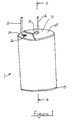
Figure 1 is a schematic perspective view of a cylindrical double layer capacitor embodying the present invention; -
Figure 2 is a cross sectional view taken along line 2-2 ofFigure 1 ; -
Figure 3 is a top perspective view of an alternative embodiment of the invention; and -
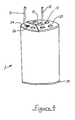
Figure 4 is a view similar toFigure 3 of another alternative embodiment of the invention. - Referring to
Figure 1 andFigure 2 , a cylindricaldouble layer capacitor 1 includes a plurality of integrally formedfirst electrode members 2 which each extend between afirst end 3 and asecond end 4. A plurality of integrally formedsecond electrode members 5 each extend between a third end 7 and afourth end 6. As shown,members 5 are interleaved withmembers 2 such that ends 7 are locatedintermediate ends adjacent members 2. An insulator in the form of permeable separators ormembranes 8 are disposed betweenadjacent members flanges 11 extend fromrespective ends 3 of eachmember 2 and electrically connect all the first members.Flanges 11 provide a site for the metallisation of particles thereupon. Those particles form aporous connection layer 12 for anelectrical terminal 13 formembers 2.Flanges 11 also form a barrier against the ingress of the particles beyondends 3. - Ends 4 of
members 2 are locatedintermediate ends 6 and 7 of theadjacent members 5. Moreover,capacitor 1 includes second contact means in the form offlanges 14 which extend fromrespective ends 6 and are electrically connected to all the second members.Flanges 14 provide a site for the metallisation of particles thereupon. These particles form aporous connection layer 15 for an electrical terminal 16 for themembers 5. Similar tolayer 12,layer 15 provides a barrier against the ingress of the particles beyondends 6 and into the capacitor. -
Members 2 are integrally connected and formed from a first continuous conductive sheet. Similarly,members 5 are integrally connected and formed from a second continuous conductive sheet. These sheets are initially coated on each side withlayers 18 of activated carbon. As will be appreciated by those skilled in the art, the activated carbon provides a large effective surface area and, as such, is a preferred material for optimising capacitance. - Once so coated, the sheets are overlapped with
membrane 8 disposed therebetween. This combination is then wound onto a hollow cylindrical former 17 to form a spiral.Flanges ends flanges inner end flanges - In a less preferred embodiment the deforming of the flanges occurs as a separate step following the winding.
-
Layers flanges arrows flanges flanges ends flanges capacitor 1. - The metal spray is produced using a "Metco" oxy-acetylene spray gun. This equipment uses a 3 mm aluminium wire feed and standard oxygen and acetylene bottles. The wire is fed between 1.4 and 1.8 cm per second, and no more than about 1 to 2 seconds dwell time is permitted on the element at a distance of 20 cm from the tip of the gun. As stated above, it is preferred that the flow of metal spray is directed toward the flanges from a position radially outwardly from the capacitor to minimise the risk of any ingress of particles. Preferably also, the gun is moved circumferentially with respect to the
cylindrical capacitor 1 to provide all the particles with a substantially uniform angle of approach to all portions of the flanges. In other embodiments, however,flanges - Movement of the spray gun is repeated three times for each of
flanges - Cooling periods are necessary since the separators may soften at temperatures of about 100 °C and may shrink in the cross direction above that temperature.
- If necessary, after spraying, either or both of
layers planar surface 24. In some embodiments, grinding or other machining is also applied between coats of the spray. This grinding or machining is carried out to ensure thatsurface 24 is sufficiently configured for anelectrical terminal 13 and 16 to be attached. In thisembodiment surface 24 does not extend over the entirety of theexterior surface 25 oflayer 12 although in other embodiments this is the case. Moreover, althoughlayer 15 will include a similar substantiallyplanar surface 24, it need not be of the same size as thesurface 24 located onlayer 12. -
Terminals 13 and 16 will typically have at one end a 10 mm wideflat tab 26 to facilitate attachment torespective surfaces 24.Tabs 26 will be pressed to a thickness of approximately 0.35 mm. - Although hidden in
Figure 1 , terminal 16 is welded radially onlayer 15 and then extends axially up the centre of former 17.Terminal 13, on the other hand, is welded tangentially acrosslayer 12. Preferably, thelayers terminals 13 and 16 respectively. - Both
terminals 13 and 16 are welded to the associated layers using laser welding equipment such as a pulsed YAG laser. Two 8 mm rows ofwelds 3 mm apart on each tab can be used as a minimum. The laser is moved at 140 mm/min while being pulsed at 10 Hz with an energy of 29.5 joules/pulse to provide sufficient energy to weld the tabs to the sprayed aluminium surface. Insufficient energy will fail to weld the tab while excess energy may cause the beam to penetrate the spray and ignite the carbon. - In
other embodiments terminals 13 and 16 are welded ultrasonically torespective layers - The construction is completed by placing the capacitor into a canister from which the terminals protrude. Electrolyte is then introduced into the capacitor through one or both of
porous layers respective flanges - Reference is now made to the alternative embodiment of the invention illustrated in
Figure 3 , where corresponding features are denoted by corresponding reference numerals. More particularly,layer 12 is substantially annular and extends over less than all of theflanges 11. Accordingly, in this embodiment use is made of anon-porous layer 12 as the electrolyte is able to ingress into the capacitor between the exposed flanges. - In other embodiments use is made of a
porous layer 12 that covers less than all of theflanges 11. That is, although a porous layer provides microscopic discontinuities, a similar effect can be achieved through provision of macroscopic discontinuities in a non-porous layer. - Another example of macroscopic discontinuities are shown in the
Figure 4 embodiment. In thisembodiment layer 12 includes a plurality of spaced apart apertures to facilitate passage of the electrolyte into the capacitor. - Metals other than aluminium are used in other embodiments if the electrolyte and operation voltage permit.
- In another alternative the entire surfaces of the top and bottom of the capacitor are metallised, for instance with a solid former. Terminals are then spot welded to the metallised ends, or caps are welded to the ends. These capacitors are connected in series by butting the metallised ends together.
- Although the invention has been described with reference to specific examples it will be appreciated by these skilled in the art that it may be embodied in many other forms within the scope of the claims.
Claims (10)
- A method for producing a double layer capacitor (1) including a plurality of first electrode members (2) each extending between a first end (3) and a second end (4) and a plurality of second electrode members (5) each extending between a third end (7) and a fourth end (6), the method including the steps of:coating first and second electrode sheets on each side with activated carbon (18);winding the first and second electrode sheets into a spiral thereby forming a plurality of integrally connected first electrode members (2) and a plurality of integrally connected second electrode members (5) whereby the second members (5) are interleaved with the first members (2) such that the third ends (7) of the second members (5) are located intermediate the first and second ends (3, 4) of the adjacent first members (2), and such that the second ends (4) of the first members (2) are located intermediate the third and fourth ends (7, 6) of the adjacent second members (5), and whereby a permeable separator (8) is disposed between the adjacent first and second members (2, 5) to prevent electrical contact therebetween;deforming the first ends (3) to form flanges for defining first contact means (11) having a site for metallisation of particles thereupon, and deforming the fourth ends (6) to form flanges for defining second contact means (14) having a site for metallisation of particles thereupon, the flanges overlying adjacent flanges to form a barrier against the ingress of said particles beyond said first and fourth ends (3, 6), while allowing an electrolyte to move between the flanges and into cavities between the members (2, 5); anddirecting a stream (21, 22) of said particles toward said sites such that said particles metallise to form first and second connection layers (12, 15) for respective electrical terminals (13, 16) for the first and second members (2, 5).
- A method according to claim 1 wherein said first connection layer (12) is porous and said method includes the further step of passing an electrolyte through said metallisation and between said interleaved members (2, 5).
- A method according to claim 2 wherein said porosity is provided by macroscopic discontinuities in said first connection layer (12).
- A method according to claim 3 wherein the first connection layer (12) includes a plurality of spaced apart discontinuities.
- A method according to claim 2 wherein said porosity is provided by microscopic discontinuities in said first connection layer (12).
- A method according to any of the preceding claims wherein said first connection layer (12) extends over less than all of the first contact means (11).
- A method according to any of the preceding claims including the step of providing at least a portion of said first connection layer (12) with a substantially planar exterior surface (24).
- A method according to any of the preceding claims including the step of attaching said terminals (13, 16) to said connection layers (12, 15).
- A method according to claim 8 wherein said step of attaching includes welding.
- A method according to claim 9 wherein said welding is by way of laser radiation.
Applications Claiming Priority (3)
| Application Number | Priority Date | Filing Date | Title |
|---|---|---|---|
| AUPO709497 | 1997-05-30 | ||
| AUPO7094A AUPO709497A0 (en) | 1997-05-30 | 1997-05-30 | Terminal connection to double layer capacitors |
| PCT/AU1998/000406 WO1998054739A1 (en) | 1997-05-30 | 1998-06-01 | An energy storage device |
Publications (3)
| Publication Number | Publication Date |
|---|---|
| EP1016107A1 EP1016107A1 (en) | 2000-07-05 |
| EP1016107A4 EP1016107A4 (en) | 2007-01-17 |
| EP1016107B1 true EP1016107B1 (en) | 2011-03-30 |
Family
ID=3801385
Family Applications (1)
| Application Number | Title | Priority Date | Filing Date |
|---|---|---|---|
| EP98923924A Expired - Lifetime EP1016107B1 (en) | 1997-05-30 | 1998-06-01 | Method for producing a double layer capacitor |
Country Status (6)
| Country | Link |
|---|---|
| US (1) | US6275372B1 (en) |
| EP (1) | EP1016107B1 (en) |
| JP (1) | JP2002500824A (en) |
| AU (1) | AUPO709497A0 (en) |
| DE (1) | DE69842205D1 (en) |
| WO (1) | WO1998054739A1 (en) |
Families Citing this family (43)
| Publication number | Priority date | Publication date | Assignee | Title |
|---|---|---|---|---|
| AR030154A1 (en) * | 1999-07-05 | 2003-08-13 | Nihon Nohyaku Co Ltd | DERIVED FROM FTALAMIDE, DERIVED FROM HETEROCICLIC AMINE USEFUL AS INTERMEDIARY FOR THE PRODUCTION OF THE SAME, AGROHORTICALLY INSECTICIDE AND METHOD TO USE SUCH INSECTICIDE |
| US7456077B2 (en) | 2000-11-03 | 2008-11-25 | Cardiac Pacemakers, Inc. | Method for interconnecting anodes and cathodes in a flat capacitor |
| US6509588B1 (en) | 2000-11-03 | 2003-01-21 | Cardiac Pacemakers, Inc. | Method for interconnecting anodes and cathodes in a flat capacitor |
| US6687118B1 (en) | 2000-11-03 | 2004-02-03 | Cardiac Pacemakers, Inc. | Flat capacitor having staked foils and edge-connected connection members |
| US7107099B1 (en) * | 2000-11-03 | 2006-09-12 | Cardiac Pacemakers, Inc. | Capacitor having a feedthrough assembly with a coupling member |
| US7355841B1 (en) | 2000-11-03 | 2008-04-08 | Cardiac Pacemakers, Inc. | Configurations and methods for making capacitor connections |
| US6699265B1 (en) | 2000-11-03 | 2004-03-02 | Cardiac Pacemakers, Inc. | Flat capacitor for an implantable medical device |
| US6684102B1 (en) * | 2000-11-03 | 2004-01-27 | Cardiac Pacemakers, Inc. | Implantable heart monitors having capacitors with endcap headers |
| AUPR194400A0 (en) * | 2000-12-06 | 2001-01-04 | Energy Storage Systems Pty Ltd | An energy storage device |
| US6643119B2 (en) * | 2001-11-02 | 2003-11-04 | Maxwell Technologies, Inc. | Electrochemical double layer capacitor having carbon powder electrodes |
| AUPS119502A0 (en) | 2002-03-19 | 2002-04-18 | Energy Storage Systems Pty Ltd | An electrolyte for an energy storage device |
| US7477941B2 (en) * | 2003-06-30 | 2009-01-13 | Johnson & Johnson Consumer Companies, Inc. | Methods of exfoliating the skin with electricity |
| US20040265395A1 (en) * | 2003-06-30 | 2004-12-30 | Ying Sun | Device for delivery of reducing agents to barrier membranes |
| US7477940B2 (en) * | 2003-06-30 | 2009-01-13 | J&J Consumer Companies, Inc. | Methods of administering an active agent to a human barrier membrane with galvanic generated electricity |
| US7479133B2 (en) * | 2003-06-30 | 2009-01-20 | Johnson & Johnson Consumer Companies, Inc. | Methods of treating acne and rosacea with galvanic generated electricity |
| US7507228B2 (en) * | 2003-06-30 | 2009-03-24 | Johnson & Johnson Consumer Companies, Inc. | Device containing a light emitting diode for treatment of barrier membranes |
| US7486989B2 (en) * | 2003-06-30 | 2009-02-03 | Johnson & Johnson Consumer Companies, Inc. | Device for delivery of oxidizing agents to barrier membranes |
| US7477938B2 (en) * | 2003-06-30 | 2009-01-13 | Johnson & Johnson Cosumer Companies, Inc. | Device for delivery of active agents to barrier membranes |
| US7477939B2 (en) * | 2003-06-30 | 2009-01-13 | Johnson & Johnson Consumer Companies, Inc. | Methods of treating a wound with galvanic generated electricity |
| US8734421B2 (en) | 2003-06-30 | 2014-05-27 | Johnson & Johnson Consumer Companies, Inc. | Methods of treating pores on the skin with electricity |
| US7476222B2 (en) * | 2003-06-30 | 2009-01-13 | Johnson & Johnson Consumer Companies, Inc. | Methods of reducing the appearance of pigmentation with galvanic generated electricity |
| US7480530B2 (en) * | 2003-06-30 | 2009-01-20 | Johnson & Johnson Consumer Companies, Inc. | Device for treatment of barrier membranes |
| US7352558B2 (en) * | 2003-07-09 | 2008-04-01 | Maxwell Technologies, Inc. | Dry particle based capacitor and methods of making same |
| US7791860B2 (en) | 2003-07-09 | 2010-09-07 | Maxwell Technologies, Inc. | Particle based electrodes and methods of making same |
| US7090946B2 (en) | 2004-02-19 | 2006-08-15 | Maxwell Technologies, Inc. | Composite electrode and method for fabricating same |
| US7224575B2 (en) * | 2004-07-16 | 2007-05-29 | Cardiac Pacemakers, Inc. | Method and apparatus for high voltage aluminum capacitor design |
| US7120008B2 (en) | 2004-07-16 | 2006-10-10 | Cardiac Pacemakers, Inc. | Method and apparatus for capacitor interconnection using a metal spray |
| DE102004034769A1 (en) * | 2004-07-19 | 2006-02-16 | Epcos Ag | Double layer capacitor, has end portions of capacitor winding layers connected via end face contact |
| US7564677B2 (en) | 2005-04-22 | 2009-07-21 | Cardiac Pacemakers, Inc. | Method and apparatus for a spacer for an electrode layer gap in a power source |
| US7327552B2 (en) | 2005-05-09 | 2008-02-05 | Cardiac Pacemakers, Inc. | Method and apparatus for electrically connecting capacitor electrodes using a spray |
| US7511941B1 (en) | 2005-06-08 | 2009-03-31 | Maxwell Technologies, Inc. | Ultrasonic sealed fill hole |
| US20060279902A1 (en) * | 2005-06-08 | 2006-12-14 | Maxwell Technologies, Inc. | Capacitor lid and housing coating design |
| US7586736B2 (en) * | 2005-07-11 | 2009-09-08 | Micro Power Electronics Inc. | Electrical insulation system and method for electrical power storage component separation |
| US20080259525A1 (en) * | 2005-11-09 | 2008-10-23 | Maxwell Technologies, Inc. | Energy storage apparatus and article of manufacture |
| JP2009529227A (en) | 2006-03-08 | 2009-08-13 | キャップ−エックス・エックス・リミテッド | Electrolytes |
| US8717740B2 (en) * | 2007-03-30 | 2014-05-06 | Nippon Chemi-Con Corporation | Electrolytic capacitor |
| US8252441B2 (en) * | 2007-08-31 | 2012-08-28 | Micro Power Electronics, Inc. | Spacers for fixing battery cells within a battery package casing and associated systems and methods |
| US8290581B2 (en) * | 2007-10-30 | 2012-10-16 | Mcneil-Ppc, Inc. | Microcurrent device with a sensory cue |
| US8150525B2 (en) * | 2008-08-27 | 2012-04-03 | Johnson & Johnson Consumer Companies, Inc. | Treatment of hyperhydrosis |
| RU2011140505A (en) | 2009-03-06 | 2013-04-20 | МакНЕЙЛ-ППС, ИНК. | ELECTRICAL STIMULATION MEANS WITH ADDITIONAL TYPES OF TOUCH IMPACT |
| US20120089232A1 (en) | 2009-03-27 | 2012-04-12 | Jennifer Hagyoung Kang Choi | Medical devices with galvanic particulates |
| CN102711905B (en) * | 2009-11-13 | 2015-06-17 | 强生消费者公司 | Galvanic skin treatment device |
| JP7645463B2 (en) | 2019-06-28 | 2025-03-14 | パナソニックIpマネジメント株式会社 | Electrolytic capacitor and its manufacturing method |
Family Cites Families (13)
| Publication number | Priority date | Publication date | Assignee | Title |
|---|---|---|---|---|
| US774115A (en) * | 1903-06-13 | 1904-11-01 | John Splitdorf | Condenser. |
| US1890312A (en) * | 1931-03-30 | 1932-12-06 | Tung Sol Condensers Inc | Condenser |
| US2107423A (en) * | 1933-03-09 | 1938-02-08 | Products Prot Corp | Electric condenser construction |
| GB619364A (en) * | 1946-12-04 | 1949-03-08 | Hunt A H Ltd | Improvements in or relating to the manufacture of metallised paper electrical capacitors |
| US2704880A (en) * | 1948-01-13 | 1955-03-29 | Joseph B Brennan | Method of making a condenser |
| US2926109A (en) * | 1954-07-07 | 1960-02-23 | Samuel E Warren | Electrode for electrolytic capacitor and methods of insulating the same |
| US3256472A (en) * | 1962-12-10 | 1966-06-14 | Gen Electric | Electrical connecting structure for rolled capacitors |
| US3891901A (en) * | 1970-02-24 | 1975-06-24 | Mallory & Co Inc P R | Capacitors with sprayed electrode terminals |
| US3665260A (en) * | 1970-06-01 | 1972-05-23 | Trw Inc | Alloy capacitor porous anodes |
| CH544992A (en) * | 1971-11-10 | 1974-01-15 | Standard Telephon & Radio Ag | Electrolytic aluminium capacitor - with one foil protruding at one roll face and metal coated by spraying |
| JPH03266407A (en) * | 1990-03-15 | 1991-11-27 | Murata Mfg Co Ltd | Film capacitor |
| US5369547A (en) * | 1993-03-22 | 1994-11-29 | The Evans Findings Co., Ltd. | Capacitor |
| JPH06349682A (en) * | 1993-06-10 | 1994-12-22 | Elna Co Ltd | Electronic components and their manufacture |
-
1997
- 1997-05-30 AU AUPO7094A patent/AUPO709497A0/en not_active Abandoned
-
1998
- 1998-06-01 DE DE69842205T patent/DE69842205D1/en not_active Expired - Lifetime
- 1998-06-01 WO PCT/AU1998/000406 patent/WO1998054739A1/en not_active Ceased
- 1998-06-01 JP JP50002199A patent/JP2002500824A/en not_active Ceased
- 1998-06-01 US US09/424,669 patent/US6275372B1/en not_active Expired - Lifetime
- 1998-06-01 EP EP98923924A patent/EP1016107B1/en not_active Expired - Lifetime
Also Published As
| Publication number | Publication date |
|---|---|
| WO1998054739A1 (en) | 1998-12-03 |
| DE69842205D1 (en) | 2011-05-12 |
| JP2002500824A (en) | 2002-01-08 |
| EP1016107A4 (en) | 2007-01-17 |
| AUPO709497A0 (en) | 1997-06-26 |
| US6275372B1 (en) | 2001-08-14 |
| EP1016107A1 (en) | 2000-07-05 |
Similar Documents
| Publication | Publication Date | Title |
|---|---|---|
| US6275372B1 (en) | Energy storage device | |
| CN110800131B (en) | Battery and method for manufacturing same | |
| KR102262668B1 (en) | Cylindrical electrochemical cells and method of manufacture | |
| EP1076371B1 (en) | Nonaqueous electrolyte secondary cells and process for fabricating same | |
| US6451473B1 (en) | Non-aqueous electrolyte secondary battery and method of manufacturing the same | |
| JP7680537B2 (en) | Subcell and manufacturing method thereof, and cylindrical secondary battery, battery pack, and automobile including the subcell | |
| EP1983595B1 (en) | Connection system for an electrochemical cell | |
| JP5590391B2 (en) | Secondary battery | |
| JP2000030731A (en) | Manufacture of electrochemical cell | |
| JP7656055B2 (en) | How the battery is manufactured | |
| US20090139082A1 (en) | Electric coupling of a connection to an electrochemical bundle | |
| KR20090132494A (en) | Electrode tab and lithium secondary battery comprising same | |
| JP3252846B2 (en) | Non-aqueous electrolyte secondary battery and method of manufacturing the same | |
| JP2000340210A (en) | Electric energy storage device | |
| KR101222284B1 (en) | Battery and method for producing the same | |
| CN112652865A (en) | Battery and battery manufacturing method | |
| CN103563153A (en) | Electrode plate group unit for secondary battery and method for manufacturing same | |
| US20150047180A1 (en) | Battery manufacturing | |
| JP2001155711A (en) | Electric energy storage device | |
| US4819115A (en) | End connections for wound capacitors and methods of making the same | |
| US20230361357A1 (en) | Power storage device | |
| US9812698B2 (en) | Method for manufacturing a connecting contact for an electrode of an electrochemical store, method for manufacturing an electrochemical store, and electrochemical store | |
| JP4428965B2 (en) | Battery unit | |
| JPS6326532B2 (en) | ||
| CN111354913A (en) | Button battery pole shell and electrode lug traceless welding method, welding structure and product |
Legal Events
| Date | Code | Title | Description |
|---|---|---|---|
| PUAI | Public reference made under article 153(3) epc to a published international application that has entered the european phase |
Free format text: ORIGINAL CODE: 0009012 |
|
| 17P | Request for examination filed |
Effective date: 19991213 |
|
| AK | Designated contracting states |
Kind code of ref document: A1 Designated state(s): DE DK FI FR GB IT SE |
|
| RAP1 | Party data changed (applicant data changed or rights of an application transferred) |
Owner name: COMMONWEALTH SCIENTIFIC AND INDUSTRIAL RESEARCH OR Owner name: ENERGY STORAGE SYSTEMS PTY, LTD |
|
| RAP1 | Party data changed (applicant data changed or rights of an application transferred) |
Owner name: ENERGY STORAGE SYSTEMS PTY, LTD |
|
| RAP1 | Party data changed (applicant data changed or rights of an application transferred) |
Owner name: ENERGY STORAGE SYSTEMS LIMITED |
|
| RAP1 | Party data changed (applicant data changed or rights of an application transferred) |
Owner name: CAP-XX LIMITED |
|
| RAP1 | Party data changed (applicant data changed or rights of an application transferred) |
Owner name: CAP-XX LIMITED |
|
| A4 | Supplementary search report drawn up and despatched |
Effective date: 20061214 |
|
| 17Q | First examination report despatched |
Effective date: 20080411 |
|
| RTI1 | Title (correction) |
Free format text: METHOD FOR PRODUCING A DOUBLE LAYER CAPACITOR |
|
| GRAP | Despatch of communication of intention to grant a patent |
Free format text: ORIGINAL CODE: EPIDOSNIGR1 |
|
| GRAS | Grant fee paid |
Free format text: ORIGINAL CODE: EPIDOSNIGR3 |
|
| GRAA | (expected) grant |
Free format text: ORIGINAL CODE: 0009210 |
|
| AK | Designated contracting states |
Kind code of ref document: B1 Designated state(s): DE DK FI FR GB IT SE |
|
| REG | Reference to a national code |
Ref country code: GB Ref legal event code: FG4D |
|
| REF | Corresponds to: |
Ref document number: 69842205 Country of ref document: DE Date of ref document: 20110512 Kind code of ref document: P |
|
| REG | Reference to a national code |
Ref country code: DE Ref legal event code: R096 Ref document number: 69842205 Country of ref document: DE Effective date: 20110512 |
|
| PG25 | Lapsed in a contracting state [announced via postgrant information from national office to epo] |
Ref country code: SE Free format text: LAPSE BECAUSE OF FAILURE TO SUBMIT A TRANSLATION OF THE DESCRIPTION OR TO PAY THE FEE WITHIN THE PRESCRIBED TIME-LIMIT Effective date: 20110330 |
|
| PG25 | Lapsed in a contracting state [announced via postgrant information from national office to epo] |
Ref country code: FI Free format text: LAPSE BECAUSE OF FAILURE TO SUBMIT A TRANSLATION OF THE DESCRIPTION OR TO PAY THE FEE WITHIN THE PRESCRIBED TIME-LIMIT Effective date: 20110330 |
|
| PLBE | No opposition filed within time limit |
Free format text: ORIGINAL CODE: 0009261 |
|
| STAA | Information on the status of an ep patent application or granted ep patent |
Free format text: STATUS: NO OPPOSITION FILED WITHIN TIME LIMIT |
|
| PG25 | Lapsed in a contracting state [announced via postgrant information from national office to epo] |
Ref country code: DK Free format text: LAPSE BECAUSE OF FAILURE TO SUBMIT A TRANSLATION OF THE DESCRIPTION OR TO PAY THE FEE WITHIN THE PRESCRIBED TIME-LIMIT Effective date: 20110330 |
|
| 26N | No opposition filed |
Effective date: 20120102 |
|
| REG | Reference to a national code |
Ref country code: DE Ref legal event code: R097 Ref document number: 69842205 Country of ref document: DE Effective date: 20120102 |
|
| PG25 | Lapsed in a contracting state [announced via postgrant information from national office to epo] |
Ref country code: IT Free format text: LAPSE BECAUSE OF FAILURE TO SUBMIT A TRANSLATION OF THE DESCRIPTION OR TO PAY THE FEE WITHIN THE PRESCRIBED TIME-LIMIT Effective date: 20110330 |
|
| PGFP | Annual fee paid to national office [announced via postgrant information from national office to epo] |
Ref country code: GB Payment date: 20140528 Year of fee payment: 17 |
|
| PGFP | Annual fee paid to national office [announced via postgrant information from national office to epo] |
Ref country code: DE Payment date: 20140528 Year of fee payment: 17 |
|
| PGFP | Annual fee paid to national office [announced via postgrant information from national office to epo] |
Ref country code: FR Payment date: 20140609 Year of fee payment: 17 |
|
| REG | Reference to a national code |
Ref country code: DE Ref legal event code: R119 Ref document number: 69842205 Country of ref document: DE |
|
| GBPC | Gb: european patent ceased through non-payment of renewal fee |
Effective date: 20150601 |
|
| REG | Reference to a national code |
Ref country code: FR Ref legal event code: ST Effective date: 20160229 |
|
| PG25 | Lapsed in a contracting state [announced via postgrant information from national office to epo] |
Ref country code: GB Free format text: LAPSE BECAUSE OF NON-PAYMENT OF DUE FEES Effective date: 20150601 Ref country code: DE Free format text: LAPSE BECAUSE OF NON-PAYMENT OF DUE FEES Effective date: 20160101 |
|
| PG25 | Lapsed in a contracting state [announced via postgrant information from national office to epo] |
Ref country code: FR Free format text: LAPSE BECAUSE OF NON-PAYMENT OF DUE FEES Effective date: 20150630 |