EP1012879B1 - Fabrication method for reduced-dimension integrated circuits - Google Patents
Fabrication method for reduced-dimension integrated circuits Download PDFInfo
- Publication number
- EP1012879B1 EP1012879B1 EP98909985A EP98909985A EP1012879B1 EP 1012879 B1 EP1012879 B1 EP 1012879B1 EP 98909985 A EP98909985 A EP 98909985A EP 98909985 A EP98909985 A EP 98909985A EP 1012879 B1 EP1012879 B1 EP 1012879B1
- Authority
- EP
- European Patent Office
- Prior art keywords
- silicon
- given
- amorphized
- successive pulses
- surface layer
- Prior art date
- Legal status (The legal status is an assumption and is not a legal conclusion. Google has not performed a legal analysis and makes no representation as to the accuracy of the status listed.)
- Expired - Lifetime
Links
Images


Classifications
-
- H—ELECTRICITY
- H10—SEMICONDUCTOR DEVICES; ELECTRIC SOLID-STATE DEVICES NOT OTHERWISE PROVIDED FOR
- H10D—INORGANIC ELECTRIC SEMICONDUCTOR DEVICES
- H10D84/00—Integrated devices formed in or on semiconductor substrates that comprise only semiconducting layers, e.g. on Si wafers or on GaAs-on-Si wafers
- H10D84/01—Manufacture or treatment
- H10D84/0123—Integrating together multiple components covered by H10D12/00 or H10D30/00, e.g. integrating multiple IGBTs
- H10D84/0126—Integrating together multiple components covered by H10D12/00 or H10D30/00, e.g. integrating multiple IGBTs the components including insulated gates, e.g. IGFETs
- H10D84/0165—Integrating together multiple components covered by H10D12/00 or H10D30/00, e.g. integrating multiple IGBTs the components including insulated gates, e.g. IGFETs the components including complementary IGFETs, e.g. CMOS devices
-
- H—ELECTRICITY
- H10—SEMICONDUCTOR DEVICES; ELECTRIC SOLID-STATE DEVICES NOT OTHERWISE PROVIDED FOR
- H10P—GENERIC PROCESSES OR APPARATUS FOR THE MANUFACTURE OR TREATMENT OF DEVICES COVERED BY CLASS H10
- H10P30/00—Ion implantation into wafers, substrates or parts of devices
- H10P30/20—Ion implantation into wafers, substrates or parts of devices into semiconductor materials, e.g. for doping
- H10P30/202—Ion implantation into wafers, substrates or parts of devices into semiconductor materials, e.g. for doping characterised by the semiconductor materials
- H10P30/204—Ion implantation into wafers, substrates or parts of devices into semiconductor materials, e.g. for doping characterised by the semiconductor materials into Group IV semiconductors
-
- H—ELECTRICITY
- H10—SEMICONDUCTOR DEVICES; ELECTRIC SOLID-STATE DEVICES NOT OTHERWISE PROVIDED FOR
- H10D—INORGANIC ELECTRIC SEMICONDUCTOR DEVICES
- H10D30/00—Field-effect transistors [FET]
- H10D30/01—Manufacture or treatment
- H10D30/021—Manufacture or treatment of FETs having insulated gates [IGFET]
- H10D30/0223—Manufacture or treatment of FETs having insulated gates [IGFET] having source and drain regions or source and drain extensions self-aligned to sides of the gate
-
- H—ELECTRICITY
- H10—SEMICONDUCTOR DEVICES; ELECTRIC SOLID-STATE DEVICES NOT OTHERWISE PROVIDED FOR
- H10D—INORGANIC ELECTRIC SEMICONDUCTOR DEVICES
- H10D62/00—Semiconductor bodies, or regions thereof, of devices having potential barriers
- H10D62/10—Shapes, relative sizes or dispositions of the regions of the semiconductor bodies; Shapes of the semiconductor bodies
- H10D62/13—Semiconductor regions connected to electrodes carrying current to be rectified, amplified or switched, e.g. source or drain regions
- H10D62/149—Source or drain regions of field-effect devices
- H10D62/151—Source or drain regions of field-effect devices of IGFETs
-
- H—ELECTRICITY
- H10—SEMICONDUCTOR DEVICES; ELECTRIC SOLID-STATE DEVICES NOT OTHERWISE PROVIDED FOR
- H10D—INORGANIC ELECTRIC SEMICONDUCTOR DEVICES
- H10D84/00—Integrated devices formed in or on semiconductor substrates that comprise only semiconducting layers, e.g. on Si wafers or on GaAs-on-Si wafers
- H10D84/01—Manufacture or treatment
- H10D84/0123—Integrating together multiple components covered by H10D12/00 or H10D30/00, e.g. integrating multiple IGBTs
- H10D84/0126—Integrating together multiple components covered by H10D12/00 or H10D30/00, e.g. integrating multiple IGBTs the components including insulated gates, e.g. IGFETs
- H10D84/0165—Integrating together multiple components covered by H10D12/00 or H10D30/00, e.g. integrating multiple IGBTs the components including insulated gates, e.g. IGFETs the components including complementary IGFETs, e.g. CMOS devices
- H10D84/017—Manufacturing their source or drain regions, e.g. silicided source or drain regions
-
- H—ELECTRICITY
- H10—SEMICONDUCTOR DEVICES; ELECTRIC SOLID-STATE DEVICES NOT OTHERWISE PROVIDED FOR
- H10D—INORGANIC ELECTRIC SEMICONDUCTOR DEVICES
- H10D84/00—Integrated devices formed in or on semiconductor substrates that comprise only semiconducting layers, e.g. on Si wafers or on GaAs-on-Si wafers
- H10D84/01—Manufacture or treatment
- H10D84/02—Manufacture or treatment characterised by using material-based technologies
- H10D84/03—Manufacture or treatment characterised by using material-based technologies using Group IV technology, e.g. silicon technology or silicon-carbide [SiC] technology
- H10D84/038—Manufacture or treatment characterised by using material-based technologies using Group IV technology, e.g. silicon technology or silicon-carbide [SiC] technology using silicon technology, e.g. SiGe
-
- H—ELECTRICITY
- H10—SEMICONDUCTOR DEVICES; ELECTRIC SOLID-STATE DEVICES NOT OTHERWISE PROVIDED FOR
- H10P—GENERIC PROCESSES OR APPARATUS FOR THE MANUFACTURE OR TREATMENT OF DEVICES COVERED BY CLASS H10
- H10P30/00—Ion implantation into wafers, substrates or parts of devices
- H10P30/20—Ion implantation into wafers, substrates or parts of devices into semiconductor materials, e.g. for doping
- H10P30/208—Ion implantation into wafers, substrates or parts of devices into semiconductor materials, e.g. for doping of electrically inactive species
-
- H—ELECTRICITY
- H10—SEMICONDUCTOR DEVICES; ELECTRIC SOLID-STATE DEVICES NOT OTHERWISE PROVIDED FOR
- H10P—GENERIC PROCESSES OR APPARATUS FOR THE MANUFACTURE OR TREATMENT OF DEVICES COVERED BY CLASS H10
- H10P32/00—Diffusion of dopants within, into or out of wafers, substrates or parts of devices
- H10P32/10—Diffusion of dopants within, into or out of semiconductor bodies or layers
- H10P32/14—Diffusion of dopants within, into or out of semiconductor bodies or layers within a single semiconductor body or layer in a solid phase; between different semiconductor bodies or layers, both in a solid phase
- H10P32/1408—Diffusion of dopants within, into or out of semiconductor bodies or layers within a single semiconductor body or layer in a solid phase; between different semiconductor bodies or layers, both in a solid phase from or through or into an external applied layer, e.g. photoresist or nitride layers
-
- H—ELECTRICITY
- H10—SEMICONDUCTOR DEVICES; ELECTRIC SOLID-STATE DEVICES NOT OTHERWISE PROVIDED FOR
- H10P—GENERIC PROCESSES OR APPARATUS FOR THE MANUFACTURE OR TREATMENT OF DEVICES COVERED BY CLASS H10
- H10P32/00—Diffusion of dopants within, into or out of wafers, substrates or parts of devices
- H10P32/10—Diffusion of dopants within, into or out of semiconductor bodies or layers
- H10P32/17—Diffusion of dopants within, into or out of semiconductor bodies or layers characterised by the semiconductor material
- H10P32/171—Diffusion of dopants within, into or out of semiconductor bodies or layers characterised by the semiconductor material being group IV material
-
- Y—GENERAL TAGGING OF NEW TECHNOLOGICAL DEVELOPMENTS; GENERAL TAGGING OF CROSS-SECTIONAL TECHNOLOGIES SPANNING OVER SEVERAL SECTIONS OF THE IPC; TECHNICAL SUBJECTS COVERED BY FORMER USPC CROSS-REFERENCE ART COLLECTIONS [XRACs] AND DIGESTS
- Y10—TECHNICAL SUBJECTS COVERED BY FORMER USPC
- Y10S—TECHNICAL SUBJECTS COVERED BY FORMER USPC CROSS-REFERENCE ART COLLECTIONS [XRACs] AND DIGESTS
- Y10S148/00—Metal treatment
- Y10S148/061—Gettering-armorphous layers
Definitions
- This invention relates to the fabrication of source drain 2 junctions of a metal oxide semiconductor field-effect transistor (MOSFET), and to the fabrication of MOSFETS on a silicon substrate, in the fabrication of integrated circuits (IC) and, more particularly, to the fabrication of IC comprising metal oxide semiconductor field-effect transistors (MOSFET) employing 100 nm and shallower junctions.
- MOSFET metal oxide semiconductor field-effect transistor
- CMOS field-effect transistors employing 0.25 ⁇ m gate length dimensions will- soon be commercially available. Fabrication of such 0.25 ⁇ m dimension FETs typically employs ion implantation for silicon doping. However, MOSFETs having reduced gate-length dimensions of only 0.18 ⁇ m and lower are currently being developed. Reduction of gate lengths necessitates source-drain junction depth scaling. For the 0.18 ⁇ m CMOS technology, these junctions depths are projected, by the Semiconductor Industry Association's "The National Technical Roadmap for Semiconductors" (1995), to be at less than 80 nm. Such junctions are difficult to form using ion implantation due to ion-channeling and transient enhanced diffusion.
- Prussin et al. J. ElectroChem. Soc., Vol. 137, No. 6 (June. 1990), pages 1912-1914; "Damage Removal/Dopant Diffusion Tradeoffs in Ultra-Shallow Implanted p + -n Junctions," by R. B. Fair, IEEE Transactions on Electron Devices, Vol. 17, No. 10 (Oct. 1990), pages 2237-2241, and "Avoiding End-of-Range Dislocations in Ion-Implanted Silicon,” by S. Acco et al., Materials Science and Engineering, B34, (1995) pages 168-174, all of which are directed to ion implantation to effect silicon amorphization.
- the present invention provides a method for fabricating source drain junctions of a MOSFET on a substrate comprising a given crystalline silicon surface layer, wherein said method comprises the steps of: (a) amorphizing silicon of said given crystalline silicon surface layer of said substrate to a given amorphization depth; and (b) thereafter depositing a given amount of doping material as a film on the surface of said given amorphized silicon surface layer; characterised by:- (c) then temporarily heating at least a portion of said given amorphized surface layer of said silicon for a certain time to a temperature which is sufficient to melt amorphized silicon but is insufficient to melt crystalline silicon to thereby result in said deposited dopant diffusing into said given melted amorphized silicon surface layer; whereby the melted silicon of said portion cools after said certain time to thereby effect a recrystallization of the silicon of said portion of said given surface layer.
- the amorphized silicon is melted at a temperature insufficient to melt crystalline silicon since the melting temperature of amorphized silicon is substantially below that of crystalline silicon.
- the fabrication method of the present invention can provide a solution to the aforesaid problem of thermal diffusion, thereby permitting P-GILD to be used for achieving ultra-shallow (e.g. less than 80nm) junction formation.
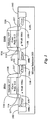
- CMOS structure comprising silicon substrate 100, isolation elements 102 and complimentary FETs 104a and 104b.
- the structure of complimentary FETs 104a and 104b differ only in that FET 104a comprises n well 106a, p + source 108a and p + drain 110a, while FET 104b comprises p well 106b, n + source 108b and n + drain 110b. In all other respects, the structure of complimentary FETs 104a and 104b is similar.
- both of complimentary FETs 104a and 104b comprise (1) gate poly 112 insulated from the well of that FET by a thin layer 114 of SiO 2 , (2) side wall spacers 116, (3) silicide electrical contacts 117 situated on top of the respective gate poly, source and drain of each of complimentary FETs 104a and 104b, and (4) shallow doped extensions 118 coupling the source and drain of each of complimentary FETs 104a and 104b to the channel region under the gate poly.
- extensions 118 which connect the deep sources and drains to the channel. Extensions 118 are needed to prevent drain induced barrier lowering (DIBL) and punchthrough.
- DIBL drain induced barrier lowering
- the extensions are currently formed by a shallow low energy implant and anneal, after which side wall spacers are formed and deep source/drains implanted.
- extensions 118 are currently formed by a relatively shallow low energy implant and, thereafter, the p + and n + sources 108a and 108b and drains 110a and 110b are formed by a relatively deep high energy ion implant.
- the already shallow junction depth of extensions 118 is reduced to less than 80 nm.
- Such a small junction depth for extensions 118 is difficult to form using ion implantation due to ion-channeling and transient enhanced diffusion.
- FIGURE 2a demonstrates only the heat diffusion pattern in that portion of the silicon of the MOSFET being fabricated that is relatively nearer to gate 202 than to the IC isolation elements.
- Prior-art P-GILD if used during the fabrication of an IC MOSFET device, would heat the entire single crystalline silicon upper surface layer 200 between adjacent IC isolation elements. Far from gate 202, the heating can be modeled using one-dimensional heat diffusion (as indicated in FIGURE 2 by solid-line arrows 204). However, the region under gate 202, which is shadowed from the laser light, remains cooler than regions far from gate 202. Hence, in the vicinity of gate 202, both vertical and lateral, thermal gradient exists.
- FIGURE 2b schematically depicts both the shadowing effect 208 and the diffraction-interference effect 210 caused by the presence of the gate 202. More particularly, within the area of the top silicon surface defined by each oblique dashed line 212 and a vertical sidewall of gate 202, the shadowing effect is schematically indicated by boxes 214 and the diffraction-interference effect is schematically indicated by boxes 216.
- FIGURE 2b demonstrates illumination effects near the gate edge. Due to the large numerical aperture of a P-GILD projection system, the angle of incidence varies from 90 to 50 degrees. As a result of angular spread of the illuminating laser light, shadowing by the gate can reduce up to 50% of the light in the region next to it. Some of the fluence loss may be compensated for by additional light reflected off of the silicon sidewall of gate 202. However, it can be shown that silicon exhibits low reflectivity of TM polarized light at near grazing angles. It can be seen that due to this low reflectivity of TM polarized light, a large amount of the light incident on the gate sidewall is in fact absorbed. Hence, reflection off gate 202 cannot completely compensate for the fluence loss due to shadowing. Further, diffraction from the edge of gate 202 and interference between the reflection off of gate 202 and the incident light reduces the incident intensity next to the edge of gate 202. This results in the near gate region being colder than the rest of the source and drain regions.
- the combination of enhanced cooling and shadowing at the gate edge can prevent the melt from extending up to the edge of gate 202.
- the melt may reach gate 202 at sufficiently high laser energies, the use of such high laser energies is undesirable.
- the negative overlap between gate 202 and the melt increases with increasing gate length due to larger thermal gradients under gate 202.
- a modern circuit may be comprised of devices with varying gate lengths. As a result, the negative overlap will vary for the different devices.
- a negative overlap results in high series resistances and large leakage to the substrate. Such junctions are unacceptable for modern CMOS technology and methods for ensuring that junctions extend to the gate for all gate lengths needs to be devised.
- two-dimensional cooling can also prevent melting near the edge of an isolation element, thereby causing a short to be created between the junction and the well when silicidation is performed. As a result, the drain cannot be biased with respect to the well. Hence, melting up to the isolation element 102 is extremely important.
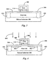
- FIGURE 3 shows a stage in the fabrication of one of the MOSFETs of FIGURE 1 just prior to the execution of fabrication steps which include the fabrication steps of the present invention shown in FIGURES 4 and 5.
- well 106, and gate poly 112 situated over a thin layer 114 of SiO 2 have already been fabricated.
- the first of the fabrication steps of the present invention comprises the step of amorphizing, to a desired ultra-shallow depth, regions of the FIGURE 1 MOSFET being fabricated which include the upper polycrystalline silicon layer 400 of gate poly 112 and the upper single crystalline silicon layers 402 of well 106.
- Amorphization may be achieved by ion implantation of a heavy atom, such as argon, silicon, and germanium (as indicated in FIGURE 4 by arrows 404).
- germanium is to be preferred because it is a heavy atom which requires low doses to amorphize silicon, produces abrupt amorphous-crystalline interfaces, and is isoelectronic in the silicon lattice.
- layer 402 on each side of gate poly 112, which is to be amorphized extends all the way to an isolation element 102.
- the desired ultra-shallow depth of the layers 400 and 402 to be amorphized is substantially 30 nm (which is less than 80 nm)
- a dose of 2 x 10 14 atoms/cm 2 is required to achieve this desired 30 nm amorphization depth.
- a 20 KeV germanium implant at a dose of 2 x 10 14 atoms/cm 2 achieves this desired 30 nm amorphization depth of the layers 400 and 402. This implant condition is easily obtainable using existing implanters.
- the amorphous depth is a function of implant dose and implant energy.
- the range of implant dose is between 1 x 10 13 atoms/cm 2 and 1 x 10 16 atoms/cm 2
- the range of implant energy is between 5 KeV atoms/cm 2 and 400 KeV.
- the amount of the dose to be incorporated in amorphized layers 400 and 402 during the second step of the known P-GILD operation depends on the amount of the given dopant compound that has been predeposited during the first step of the known P-GILD operation.
- FIGURE 5 there is shown the second step of the P-GILD operation, which takes place at the completion of the aforesaid two unshown fabrication steps.
- excimer laser radiation 502. this excimer laser radiation may be derived from an ArF excimer laser producing radiation at a wavelength of 193 nm (as taught in the T. Akane et al. article), it also may be derived from other types of lasers (e.g., a 248 nm KrF laser, a 351 nm XeF laser, or a 308 nm XeCl laser).
- Applicant has employed a pulsed XeCl excimer laser producing radiation at a wavelength of 308 nm for performing the aforesaid second step of the P-GILD operation.
- amorphous silicon has a factor of 10 lower thermal conductivity, a 300 °C lower melt temperature, and a 30 percent lower reflectivity than crystalline silicon. The combination of these effects lowers the melt threshold of amorphous silicon compared to crystalline silicon.
- the depth of the amorphized layers is limited to that needed for the regions to be occupied by each of these extensions.
- the second step of the P-GILD operation used in lightly doping the regions of extensions 118, results in the amorphized layers of silicon melting right up to the edge of gate poly 112, due to the significant reduction in the thermal conductivity and melt temperature of these amorphized layers.
- the second step of the P-GILD operation comprises each of successive pulses of laser radiation. The irradiating energy of each of the successive pulses is sufficient to cause melting of an amorphized silicon spot, but is insufficient to cause melting of a crystalline silicon spot.
- the now-doped melted silicon thereof immediately cools and recrystallizes. Therefore, the irradiation by a first pulse of a given amorphized silicon spot that overlaps the recrystallized silicon of an already irradiated spot will not cause any remelting of the recrystallized silicon, but will result only in the melting of the given amorphized silicon spot. Further, a large energy window exists where melting will not extend beyond the amorphous regions, since the liquid silicon is highly undercooled and cannot produce further silicon melting. Hence, amorphization can be used to define the melt depth.
- layer 400 of gate poly 112 is both amorphized and doped.
- a masking layer over gate poly 112 may be employed during the amorphization implanting step of FIGURE 4, thereby preventing gate melting of gate poly 112 to take place during the second step of the P-GILD operation.
- P-GILD P-GILD
- higher energy e.g. 40 KeV
- higher dose e.g. 6 x 10 14 atoms/cm 2 germanium implants.
- the two steps of P-GILD are used to provide (1) appropriate deposited concentrations of films of doping material during the first of these two steps, and (2) appropriate pulsed laser energy to effect melting of only the amorphised source and drain regions during the second of these two steps.
- the fabrication of the deep source and drain involve the reamorphization of the already-fabricated ultra-shallow (i.e., less than 100 nm depth) junctions, since these already-fabricated ultra-shallow junctions extend all the way to side wall spacers 116.
- the extent of the ultra-shallow junctions may be limited to solely the locations of the extensions and, therefore, not include the locations of the deep source and drain.
- the amorphization for the source and drain locations is independent of the amorphization for the extension locations, so that the amorphization for the source and drain locations may occur either before or after the amorphization for the extension locations.
- the present invention may be employed for fabricating only the extensions of an MOSFET or, alternatively, only the deep source and drain of an MOSFET, rather than both of these.
- amorphization implants produce supersaturation of point defects.
- point defect injection results in nucleation of extended defects.
- a critical annealing temperature ordinarily is required to anneal out the extended defects.
- This ordinarily required anneal for the first amorphization implant, shown in FIGURE 4 and described above, is at 1050 °C for 10 sec.
- the laser melting of the amorphized silicon by the second step of the P-GILD operation inherently provides a certain amount of annealing.
- the junctions are not likely to move much as a result of this thermal cycle. Therefore, in this case, no additional anneal for laser annealed junctions may be necessary.
- the exact extent of the diffusion after laser annealing needs to be determined experimentally in order to determine if any additional annealing is necessary.
Landscapes
- Insulated Gate Type Field-Effect Transistor (AREA)
- Metal-Oxide And Bipolar Metal-Oxide Semiconductor Integrated Circuits (AREA)
Abstract
Description
- This invention relates to the fabrication of source drain 2 junctions of a metal oxide semiconductor field-effect transistor (MOSFET), and to the fabrication of MOSFETS on a silicon substrate, in the fabrication of integrated circuits (IC) and, more particularly, to the fabrication of IC comprising metal oxide semiconductor field-effect transistors (MOSFET) employing 100 nm and shallower junctions.
- CMOS field-effect transistors (FET) employing 0.25 µm gate length dimensions will- soon be commercially available. Fabrication of such 0.25 µm dimension FETs typically employs ion implantation for silicon doping. However, MOSFETs having reduced gate-length dimensions of only 0.18 µm and lower are currently being developed. Reduction of gate lengths necessitates source-drain junction depth scaling. For the 0.18 µm CMOS technology, these junctions depths are projected, by the Semiconductor Industry Association's "The National Technical Roadmap for Semiconductors" (1995), to be at less than 80 nm. Such junctions are difficult to form using ion implantation due to ion-channeling and transient enhanced diffusion.
- The article "Two-Step Doping Using Excimer Laser in Boron Doping of Silicon," by T. Akane et al., Jpn. J. Appl. Phys. Vol. 31 (Dec. 1992) Pt. 1, No. 12B, pages 4437-4440 discloses an alternative means for silicon doping. In this regard, one is further referred to the articles "A Shallow Junction Submicrometer PMOS Process Without High-Temperature Anneals," by P. G. Carey et al., IEEE Electron Device Letters, Vol. 9, No. 10, (Oct. 1988), pages 542-544, "Role of Ion Mass, Implant Dose, and Wafer Temperature on End-of-Range Defects," by S. Prussin et al., J. ElectroChem. Soc., Vol. 137, No. 6 (June. 1990), pages 1912-1914; "Damage Removal/Dopant Diffusion Tradeoffs in Ultra-Shallow Implanted p+-n Junctions," by R. B. Fair, IEEE Transactions on Electron Devices, Vol. 17, No. 10 (Oct. 1990), pages 2237-2241, and "Avoiding End-of-Range Dislocations in Ion-Implanted Silicon," by S. Acco et al., Materials Science and Engineering, B34, (1995) pages 168-174, all of which are directed to ion implantation to effect silicon amorphization.
- Were it not for the high thermal conduction in crystalline silicon, ultra-shallow (e.g., less than 100 nm) junction formation would be possible using prior-art projection gas immersion laser doping (P-GILD), due to near surface absorption of the laser light and short laser pulse widths. In this regard, the geometry of an MOSFET device being fabricated results in shadowing and diffraction of the laser light illuminating the device's surface which has a large effect on thermal loading. Unfortunately, the high thermal conduction in crystalline silicon acts to reduce the junction depth at the edges. These thermal conduction effects become apparent as the dimensions of the doped regions approach the thermal diffusion lengths. As a result, the attributes of the doped region are a function of their.dimensions and the surrounding geometry. In the case of source/drain doping in a CMOS device, this results in the doped regions not extending up to the gate (negative gate overlap) or the isolation. This presents an unacceptable problem, since device performance suffers due to high parasitic resistances and shorts between the junctions and the wells.
- DE-A-19505818 discloses the features of the precharacterising portion of claim 1.
- The present invention provides a method for fabricating source drain junctions of a MOSFET on a substrate comprising a given crystalline silicon surface layer, wherein said method comprises the steps of: (a) amorphizing silicon of said given crystalline silicon surface layer of said substrate to a given amorphization depth; and (b) thereafter depositing a given amount of doping material as a film on the surface of said given amorphized silicon surface layer; characterised by:- (c) then temporarily heating at least a portion of said given amorphized surface layer of said silicon for a certain time to a temperature which is sufficient to melt amorphized silicon but is insufficient to melt crystalline silicon to thereby result in said deposited dopant diffusing into said given melted amorphized silicon surface layer; whereby the melted silicon of said portion cools after said certain time to thereby effect a recrystallization of the silicon of said portion of said given surface layer.
- During the heating step the amorphized silicon is melted at a temperature insufficient to melt crystalline silicon since the melting temperature of amorphized silicon is substantially below that of crystalline silicon.
- The fabrication method of the present invention can provide a solution to the aforesaid problem of thermal diffusion, thereby permitting P-GILD to be used for achieving ultra-shallow (e.g. less than 80nm) junction formation.
- An embodiment of the present invention will now be described, by way of example only, with reference to the accompanying drawings, in which:-
- FIGURE 1 diagrammatically shows the structure of two FETs that have been fabricated in accordance with modern silicon CMOS technology;
- FIGURE 2a diagrammatically shows the pattern of heat diffusion from the heated upper region of an MOSFET that occurs when P-GILD is used in its fabrication;
- FIGURE 2b diagrammatically shows the shadowing and diffraction-interference effects caused by the gate polycrystalline (poly) structure of an MOSFET that occurs when P-GILD is used in its fabrication;
- FIGURE 3 diagrammatically shows the structure of one of the two FIGURE 1 MOSFETs that is to be fabricated in accordance with the method steps of the present invention at a stage in the fabrication of that FET which occurs prior to either the doping of its extensions or the doping of its source or drain, but subsequent to the doping of its well;
- FIGURE 4 diagrammatically shows a fabrication step of the present invention comprising surface amorphizing by ion implantating the silicon forming the upper region of the MOSFET of FIGURE 3; and
- FIGURE 5 diagrammatically shows a fabrication doping step of the present invention (which occurs subsequent to both the FIGURE 4 fabrication step of surface amorphization and other intervening fabrication steps that include radiation from a first laser operation having been used to photolytically predeposit a film of doping material) which uses the radiation from a second laser to effect a doping which includes both the extensions and the gate poly of that FET with the predeposited film of doping material.
-
- Referring to FIGURE 1, there is shown CMOS structure comprising
silicon substrate 100,isolation elements 102 andcomplimentary FETs complimentary FETs p well 106b, n+ source 108b and n+ drain 110b. In all other respects, the structure ofcomplimentary FETs complimentary FETs gate poly 112 insulated from the well of that FET by athin layer 114 of SiO2, (2)side wall spacers 116, (3) silicideelectrical contacts 117 situated on top of the respective gate poly, source and drain of each ofcomplimentary FETs extensions 118 coupling the source and drain of each ofcomplimentary FETs - It is apparent from FIGURE 1 that the shallowest junctions are
extensions 118, which connect the deep sources and drains to the channel.Extensions 118 are needed to prevent drain induced barrier lowering (DIBL) and punchthrough. The extensions are currently formed by a shallow low energy implant and anneal, after which side wall spacers are formed and deep source/drains implanted. - At this time, the smallest gate dimensions soon to be employed in the commercial fabrication of MOSFET structures is 0.25 µm In this case,
extensions 118 are currently formed by a relatively shallow low energy implant and, thereafter, the p+ and n+ sources 108a and 108b anddrains extensions 118 is reduced to less than 80 nm. Such a small junction depth forextensions 118 is difficult to form using ion implantation due to ion-channeling and transient enhanced diffusion. - As discussed above in the Background of the Invention section, problems that result from the high thermal conduction in crystalline silicon have prevented the prior-art P-GILD doping technique from being used in place of ion implantation to form less than a 80 nm deep junction for each of
extensions 118. - FIGURE 2a demonstrates only the heat diffusion pattern in that portion of the silicon of the MOSFET being fabricated that is relatively nearer to
gate 202 than to the IC isolation elements. Prior-art P-GILD, if used during the fabrication of an IC MOSFET device, would heat the entire single crystalline siliconupper surface layer 200 between adjacent IC isolation elements. Far fromgate 202, the heating can be modeled using one-dimensional heat diffusion (as indicated in FIGURE 2 by solid-line arrows 204). However, the region undergate 202, which is shadowed from the laser light, remains cooler than regions far fromgate 202. Hence, in the vicinity ofgate 202, both vertical and lateral, thermal gradient exists. This results in 2-D thermal diffusion in the vicinity of gate 202 (as indicated in FIGURE 2a by dashed-line arrows 206). Therefore, cooling is enhanced in this vicinity, leading to shallower or no melting, should prior-art P-GILD laser radiation be employed in the fabrication of the FET. - Further, although not shown in FIGURE 2a, it is apparent that a two-dimensional heat diffusion pattern would also exist during the fabrication of each of the CMOS FETs of FIGURE 1 at the junction of that FET's source and drain regions with an isolation element, if prior-art P-GILD laser radiation were employed in its fabrication.
- FIGURE 2b schematically depicts both the shadowing
effect 208 and the diffraction-interference effect 210 caused by the presence of thegate 202. More particularly, within the area of the top silicon surface defined by each obliquedashed line 212 and a vertical sidewall ofgate 202, the shadowing effect is schematically indicated byboxes 214 and the diffraction-interference effect is schematically indicated byboxes 216. - FIGURE 2b demonstrates illumination effects near the gate edge. Due to the large numerical aperture of a P-GILD projection system, the angle of incidence varies from 90 to 50 degrees. As a result of angular spread of the illuminating laser light, shadowing by the gate can reduce up to 50% of the light in the region next to it. Some of the fluence loss may be compensated for by additional light reflected off of the silicon sidewall of
gate 202. However, it can be shown that silicon exhibits low reflectivity of TM polarized light at near grazing angles. It can be seen that due to this low reflectivity of TM polarized light, a large amount of the light incident on the gate sidewall is in fact absorbed. Hence, reflection offgate 202 cannot completely compensate for the fluence loss due to shadowing. Further, diffraction from the edge ofgate 202 and interference between the reflection off ofgate 202 and the incident light reduces the incident intensity next to the edge ofgate 202. This results in the near gate region being colder than the rest of the source and drain regions. - Thus, the combination of enhanced cooling and shadowing at the gate edge can prevent the melt from extending up to the edge of
gate 202. Although it is possible for the melt to reachgate 202 at sufficiently high laser energies, the use of such high laser energies is undesirable. Further, the negative overlap betweengate 202 and the melt increases with increasing gate length due to larger thermal gradients undergate 202. A modern circuit may be comprised of devices with varying gate lengths. As a result, the negative overlap will vary for the different devices. A negative overlap results in high series resistances and large leakage to the substrate. Such junctions are unacceptable for modern CMOS technology and methods for ensuring that junctions extend to the gate for all gate lengths needs to be devised. - In addition, two-dimensional cooling can also prevent melting near the edge of an isolation element, thereby causing a short to be created between the junction and the well when silicidation is performed. As a result, the drain cannot be biased with respect to the well. Hence, melting up to the
isolation element 102 is extremely important. - The relatively simple process performed by the method of the present invention, shown in FIGURES 3-5 and described below, avoids the aforesaid problems of negative overlay due to two-dimensional cooling and reduction in laser fluence due to shadowing and diffraction-interference, which problems are encountered when prior-art P-GILD laser radiation is employed in the fabrication of the MOSFETs of FIGURE 1.
- FIGURE 3 shows a stage in the fabrication of one of the MOSFETs of FIGURE 1 just prior to the execution of fabrication steps which include the fabrication steps of the present invention shown in FIGURES 4 and 5. At the fabrication stage shown in FIGURE 3, well 106, and
gate poly 112 situated over athin layer 114 of SiO2 have already been fabricated. - The first of the fabrication steps of the present invention, shown in FIGURE 4, comprises the step of amorphizing, to a desired ultra-shallow depth, regions of the FIGURE 1 MOSFET being fabricated which include the upper
polycrystalline silicon layer 400 ofgate poly 112 and the upper single crystalline silicon layers 402 ofwell 106. Amorphization may be achieved by ion implantation of a heavy atom, such as argon, silicon, and germanium (as indicated in FIGURE 4 by arrows 404). However, germanium is to be preferred because it is a heavy atom which requires low doses to amorphize silicon, produces abrupt amorphous-crystalline interfaces, and is isoelectronic in the silicon lattice. - More particularly, as shown in FIGURE 4,
layer 402 on each side ofgate poly 112, which is to be amorphized, extends all the way to anisolation element 102. Assuming, by way of example, that the desired ultra-shallow depth of thelayers layers - As is known (see the aforesaid R. B. Fair article, the amorphous depth is a function of implant dose and implant energy. Depending on the desired amorphous depth, the range of implant dose is between 1 x 10¹³ atoms/cm2 and 1 x 10¹⁶ atoms/cm2, while the range of implant energy is between 5 KeV atoms/cm2 and 400 KeV.
- Subsequent to the completion of the silicon amorphization fabrication step of FIGURE 4, two fabrication steps (neither of which is shown in the drawing) take place which comprise (1) the removal of
thin layer 300 of SiO2, followed by (2) the first step of a known P-GILD operation (e. g., that disclosed above in the article "Two-Step Doping Using Excimer Laser in Boron Doping of Silicon," by T. Akane et al.) which uses an ArF excimer laser (l = 193 nm) to decompose, presumably by photolytic decomposition, a given dopant compound in gaseous form to thereby cause a film of doping material in solid form to be predeposited on the upper surfaces of the MOSFET being fabricated. The amount of the dose to be incorporated inamorphized layers - Referring to FIGURE 5, there is shown the second step of the P-GILD operation, which takes place at the completion of the aforesaid two unshown fabrication steps. As shown in FIGURE 5,
predeposited film 500 of doping material on the upper surfaces oflayers excimer laser radiation 502. While this excimer laser radiation may be derived from an ArF excimer laser producing radiation at a wavelength of 193 nm (as taught in the T. Akane et al. article), it also may be derived from other types of lasers (e.g., a 248 nm KrF laser, a 351 nm XeF laser, or a 308 nm XeCl laser). Applicant has employed a pulsed XeCl excimer laser producing radiation at a wavelength of 308 nm for performing the aforesaid second step of the P-GILD operation. - More particularly, amorphous silicon has a factor of 10 lower thermal conductivity, a 300 °C lower melt temperature, and a 30 percent lower reflectivity than crystalline silicon. The combination of these effects lowers the melt threshold of amorphous silicon compared to crystalline silicon.
- Referring again to FIGURE 1, in the process for forming
extensions 118, the depth of the amorphized layers is limited to that needed for the regions to be occupied by each of these extensions. Thereafter, the second step of the P-GILD operation, used in lightly doping the regions ofextensions 118, results in the amorphized layers of silicon melting right up to the edge ofgate poly 112, due to the significant reduction in the thermal conductivity and melt temperature of these amorphized layers. More specifically, the second step of the P-GILD operation comprises each of successive pulses of laser radiation. The irradiating energy of each of the successive pulses is sufficient to cause melting of an amorphized silicon spot, but is insufficient to cause melting of a crystalline silicon spot. After the completion of the first irradiation of a particular spot by a laser pulse, the now-doped melted silicon thereof immediately cools and recrystallizes. Therefore, the irradiation by a first pulse of a given amorphized silicon spot that overlaps the recrystallized silicon of an already irradiated spot will not cause any remelting of the recrystallized silicon, but will result only in the melting of the given amorphized silicon spot. Further, a large energy window exists where melting will not extend beyond the amorphous regions, since the liquid silicon is highly undercooled and cannot produce further silicon melting. Hence, amorphization can be used to define the melt depth. - While the fluence range for laser irradiation extends all the way from 0.05 Joules per cm2 and 1.0 Joules per cm2, the most likely radiation fluence sufficient to heat amorphized silicon to its melting temperature, but insufficient to heat crystalline silicon to its melting temperature, is 0.4 Joules per cm2.
- As indicated in FIGURES 4 and 5,
layer 400 ofgate poly 112 is both amorphized and doped. In the case that doping ofgate poly 112 is not desired, a masking layer overgate poly 112 may be employed during the amorphization implanting step of FIGURE 4, thereby preventing gate melting ofgate poly 112 to take place during the second step of the P-GILD operation. - While the use of two steps of P-GILD following silicon preamphorization is particularly suitable for fabricating the ultra-shallow (i.e., less than 100 nm depth) junctions of
extensions 118, as described above, the same two steps of P-GILD following silicon preamphorization may be used to dope the deep source and drain regions of a MOSFET being fabricated. Specifically, following the fabrication of the ultra-shallow junctions ofextensions 118,side wall spacers 116 are fabricated. Thereafter, each the deep source and drain regions located between eachside wall spacer 116 and anisolation element 102 is reamorphized to its greater desired depth than the depth of the above-described original amorphization thereof. This may be accomplished with higher energy (e.g., 40 KeV) and higher dose (e.g., 6 x 10¹⁴ atoms/cm2 germanium implants). Following such reamorphization, the two steps of P-GILD are used to provide (1) appropriate deposited concentrations of films of doping material during the first of these two steps, and (2) appropriate pulsed laser energy to effect melting of only the amorphised source and drain regions during the second of these two steps. - One reason for employing the steps of the present invention described in the preceding paragraph for doping the deep source and drain, rather than conventional ion-implant doping, is that the doping depth is more precisely controlled. An additional reason is that it is less expensive.
- In the method of the preferred embodiment of the present invention described above, the fabrication of the deep source and drain involve the reamorphization of the already-fabricated ultra-shallow (i.e., less than 100 nm depth) junctions, since these already-fabricated ultra-shallow junctions extend all the way to
side wall spacers 116. However, it should be understood that the extent of the ultra-shallow junctions may be limited to solely the locations of the extensions and, therefore, not include the locations of the deep source and drain. In this case, the amorphization for the source and drain locations is independent of the amorphization for the extension locations, so that the amorphization for the source and drain locations may occur either before or after the amorphization for the extension locations. Furthermore, the present invention may be employed for fabricating only the extensions of an MOSFET or, alternatively, only the deep source and drain of an MOSFET, rather than both of these. - As known, amorphization implants produce supersaturation of point defects. Upon annealing, point defect injection results in nucleation of extended defects. A critical annealing temperature ordinarily is required to anneal out the extended defects. This ordinarily required anneal for the first amorphization implant, shown in FIGURE 4 and described above, is at 1050 °C for 10 sec. However, the laser melting of the amorphized silicon by the second step of the P-GILD operation inherently provides a certain amount of annealing. Further, due to the small number of point defects present after the laser process, the junctions are not likely to move much as a result of this thermal cycle. Therefore, in this case, no additional anneal for laser annealed junctions may be necessary. However, in any given case, the exact extent of the diffusion after laser annealing needs to be determined experimentally in order to determine if any additional annealing is necessary.
Claims (17)
- A method of fabricating source drain junctions of a MOSFET on a substrate (100) comprising a given crystalline silicon surface layer (402), wherein said method comprises the steps of:whereby the melted silicon of said portion cools after said certain time to thereby effect a recrystallization of the silicon of said portion of said given surface layer (402).(a) amorphizing silicon of said given crystalline silicon surface layer (402) of said substrate to a given amorphization depth; and(b) thereafter depositing a given amount of doping material as a film (500) on the surface of said given amorphized silicon surface layer (402); characterised by:-(c) then temporarily heating at least a portion of said given amorphized surface layer (402) of said silicon for a certain time to a temperature which is sufficient to melt amorphized silicon but is insufficient to melt crystalline silicon to thereby result in said deposited dopant diffusing into said given melted amorphized silicon surface layer (402);
- The method defined in Claim 1, wherein said given amorphized depth of silicon overlies crystalline silicon.
- The method defined in Claim 1, wherein step (a) comprises the step of:(d) amorphizing said given surface layer (402) of said silicon to a given amorphization depth by implanting thereinto, at a given concentration per unit area, atoms of an appropriate element which are isoelectronic in the silicon lattice and at least as heavy as silicon atoms and that have been ionised and accelerated to a given energy by an ion implanter.
- The method defined in Claim 3, wherein said element is germanium.
- The method defined in Claim 3, wherein said given concentration per unit area is between 1 x 10¹³ and 1 x 10¹⁶ atoms/cm2 and said given energy is between 5 and 400 KeV.
- The method of claim 5 wherein said given concentration is 6 x 10¹⁴ atoms/cm2 and said given energy is 40KeV.
- The method defined in Claim 1, wherein step (b) comprises the step of:(d) employing radiation (502) from of a laser to decompose a given dopant compound in gaseous form to thereby cause said given amount of doping material to be deposited in solid form as said film (500) on the surface of said given amorphized silicon surface layer (402).
- The method defined in Claim 1, wherein step (c) comprises the step of:(d) employing a given amount of radiant fluence from a laser to effect said temporary heating of at least said portion of said given amorphized surface layer (402) of said silicon.
- The method defined in Claim 8, wherein said given amount of radiant fluence from said laser is 0.4 Joules per cm2.
- The method defined in Claim 8, wherein step (d) comprises the step of:(e) applying a single one of successive pulses of radiant energy from a pulsed laser to an irradiated area of said given amorphized surface layer (402) of said silicon for heating said area for the duration of that single one of said successive pulses, the radiation energy of that single one of said successive pulses being sufficient to heat the amorphized silicon of said area irradiated thereby to its melting temperature, but insufficient to heat crystalline silicon to its melting temperature.
- A method for fabricating MOSFETs on a silicon substrate (100), wherein adjacent FETs are separated from one another by isolation elements (102) and each fabricated FET comprises (i) a polycrystalline silicon gate (112) built up over (ii) the surface of an appropriately-doped single crystalline silicon well (106), (iii) first and second sidewall spacers situated, respectively, on either side of said polycrystalline silicon gate (112), (iv) a relatively deep appropriately-doped single crystalline silicon source extending longitudinally from a first isolation element (102) to the vicinity of the distal edge of said first sidewall spacer, (v) a relatively deep appropriately-doped single crystalline silicon drain extending longitudinally from a second isolation element (102) to the vicinity of the distal edge of said. second sidewall spacer, (vi) a first ultra-shallow, lightly-doped single crystalline silicon extension situated under said first sidewall spacer for connecting said source to a gate edge proximate thereto, and (vii) a second ultra-shallow, lightly-doped single crystalline silicon extension situated under said second sidewall spacer for connecting said drain to a gate edge proximate thereto; wherein said method comprises the following steps for fabricating each of said first and second ultra-shallow, doped single crystalline silicon extensions subsequent to the fabrication of said well (106) and said polycrystalline silicon gate (112) and prior to the fabrication of said first and second sidewall spacers:wherein step (a) comprises ion implanting atoms in each of first and second surface layers (402) of said single crystalline silicon well (106) that extend longitudinally from a gate edge of said polycrystalline silicon gate (112) to an isolation element (102) at a given concentration per unit area and at a given energy which results in amorphizing said first and second layers (402) to a certain depth which is less than 100 nm deep;comprising the method of claim 1,
wherein in step (b) said doping material is for doping said extensions as a film (500) in solid form on said first and second amorphized surface layers (402) by decomposing a given dopant compound in gaseous form with radiation (502) from a laser;
wherein step (c) comprises first applying the first of two successive pulses of radiant energy from a pulsed laser to a first of two overlapping irradiated areas of said given amorphized surface layer (402) of said silicon for heating said first area for the duration of said first of said successive pulses, and thereafter applying the second of said two successive pulses of radiant energy from said pulsed laser to a second of said two overlapping irradiated areas of said given amorphized surface layer (402) of said silicon for heating said second area for the duration of said second of said successive pulses, the radiation energy of each separate one of said first and second successive pulses being sufficient to heat the amorphized silicon of said area irradiated thereby to its melting temperature, but insufficient to heat crystalline silicon to its melting temperature; and the method further comprises;(d) providing a time interval between the application of said first of said two successive pulses and the application of said second of said two successive pulses that is long enough to permit the melted amorphized silicon of said first of said two overlapping areas to cool and recrystallize prior to the application of said second of said two successive pulses to the amorphized silicon of said second of said two overlapping areas. - The method defined in Claim 3, or Claim 11, wherein said given concentration per unit area of said ion-implanted atoms is between 1 x 10¹³ and 1 x 10¹⁶ atoms/cm2 and said given energy is between 5 and 400 KeV.
- The method defined in Claim 12, wherein said ion implanted atoms are germanium.
- The method defined in Claim 12, wherein:said given concentration per unit area of said ion-implanted germanium atoms is between 1 x 10¹³ and 1 x 10¹⁶ atoms/cm2 and said given energy is between 5 and 400 KeV;whereby the amorphized depth of said first and second layers (402) is less than 80 nm.
- The method defined in Claim 11, further wherein step (a) further comprises ion implanting germanium atoms in an upper surface layer (400) of said polycrystalline silicon gate (112) at a given concentration per unit area and at a given energy which results in amorphizing said upper surface layer (400) of said polycrystalline silicon gate (112) to a certain depth which is 30 nm deep.
- The method defined in Claim 11, further comprising the following steps for fabricating each of said relatively deep appropriately-doped single crystalline silicon source and drain subsequent to the fabrication of said first and second sidewall spacers:(a) ion implanting atoms at a concentration of 6 x 10¹⁴ atoms/cm2 and at an energy of 40 KeV in each of (i) a source layer of said single crystalline silicon that extends longitudinally from an edge of said first sidewall spacer to an isolation element and (ii) a drain layer of said single crystalline silicon that extends longitudinally from an edge of said second sidewall spacer to an isolation element (102), which results in amorphizing said source and drain layers (402) to the relatively deep depth required for said source and drain;(b) depositing a given amount of doping material for appropriately doping said source and drain layers (402) as a film (500) in solid form on the surface of said amorphized source and drain layers (402) by photolytically decomposing a given dopant compound in gaseous form with radiation (502) from of a laser;(c) first applying the first of two successive pulses of radiant energy from a pulsed laser to a first irradiated area of a certain one of said source and drain amorphized layers (402) of said silicon for heating said first area for the duration of said first of said successive pulses, and thereafter applying the second of said two successive pulses of radiant energy from said pulsed laser to a second irradiated area of said certain one of said source and drain amorphized layers (402) of said silicon that at least partially overlaps said first irradiated area for heating said second area for the duration of said second of said successive pulses, the radiation energy of each separate one of said first and second successive pulses being sufficient to heat the amorphized silicon of said area irradiated thereby to its melting temperature, but insufficient to heat crystalline silicon to its melting temperature; and(d) providing a time interval between the application of said first of said two successive pulses and the application of said second of said two successive pulses that is long enough to permit the melted amorphized silicon of said first area to cool and recrystallize prior to the application of said second of said two successive pulses to the amorphized silicon of said second area.
- The method defined in Claim 16, further comprising:(e) repeating steps (c) and (d) for the other of said source and drain amorphized layers (402) of said silicon from said certain one thereof.
Applications Claiming Priority (3)
| Application Number | Priority Date | Filing Date | Title |
|---|---|---|---|
| US08/792,107 US5908307A (en) | 1997-01-31 | 1997-01-31 | Fabrication method for reduced-dimension FET devices |
| US792107 | 1997-01-31 | ||
| PCT/US1998/001942 WO1998034268A2 (en) | 1997-01-31 | 1998-01-29 | Fabrication method for reduced-dimension integrated circuits |
Publications (3)
| Publication Number | Publication Date |
|---|---|
| EP1012879A2 EP1012879A2 (en) | 2000-06-28 |
| EP1012879A4 EP1012879A4 (en) | 2000-06-28 |
| EP1012879B1 true EP1012879B1 (en) | 2002-09-04 |
Family
ID=25155818
Family Applications (1)
| Application Number | Title | Priority Date | Filing Date |
|---|---|---|---|
| EP98909985A Expired - Lifetime EP1012879B1 (en) | 1997-01-31 | 1998-01-29 | Fabrication method for reduced-dimension integrated circuits |
Country Status (6)
| Country | Link |
|---|---|
| US (1) | US5908307A (en) |
| EP (1) | EP1012879B1 (en) |
| JP (1) | JP2001509316A (en) |
| KR (1) | KR100511765B1 (en) |
| DE (1) | DE69807718T2 (en) |
| WO (1) | WO1998034268A2 (en) |
Families Citing this family (85)
| Publication number | Priority date | Publication date | Assignee | Title |
|---|---|---|---|---|
| US6361951B1 (en) * | 1995-06-27 | 2002-03-26 | The University Of North Carolina At Chapel Hill | Electrochemical detection of nucleic acid hybridization |
| IT1289524B1 (en) * | 1996-12-24 | 1998-10-15 | Sgs Thomson Microelectronics | MEMORY CELL FOR EEPROM TYPE DEVICES AND RELATED MANUFACTURING PROCESS |
| US6037640A (en) * | 1997-11-12 | 2000-03-14 | International Business Machines Corporation | Ultra-shallow semiconductor junction formation |
| US5956603A (en) * | 1998-08-27 | 1999-09-21 | Ultratech Stepper, Inc. | Gas immersion laser annealing method suitable for use in the fabrication of reduced-dimension integrated circuits |
| US6355543B1 (en) * | 1998-09-29 | 2002-03-12 | Advanced Micro Devices, Inc. | Laser annealing for forming shallow source/drain extension for MOS transistor |
| US6297115B1 (en) * | 1998-11-06 | 2001-10-02 | Advanced Micro Devices, Inc. | Cmos processs with low thermal budget |
| US6184112B1 (en) * | 1998-12-02 | 2001-02-06 | Advanced Micro Devices, Inc. | Method of forming a MOSFET transistor with a shallow abrupt retrograde dopant profile |
| US6265291B1 (en) | 1999-01-04 | 2001-07-24 | Advanced Micro Devices, Inc. | Circuit fabrication method which optimizes source/drain contact resistance |
| US6771895B2 (en) * | 1999-01-06 | 2004-08-03 | Mattson Technology, Inc. | Heating device for heating semiconductor wafers in thermal processing chambers |
| US6395624B1 (en) * | 1999-02-22 | 2002-05-28 | International Business Machines Corporation | Method for forming implants in semiconductor fabrication |
| US6521501B1 (en) * | 1999-05-11 | 2003-02-18 | Advanced Micro Devices, Inc. | Method of forming a CMOS transistor having ultra shallow source and drain regions |
| US6265293B1 (en) | 1999-08-27 | 2001-07-24 | Advanced Micro Devices, Inc. | CMOS transistors fabricated in optimized RTA scheme |
| US6284630B1 (en) * | 1999-10-20 | 2001-09-04 | Advanced Micro Devices, Inc. | Method for fabrication of abrupt drain and source extensions for a field effect transistor |
| US6090651A (en) * | 1999-11-05 | 2000-07-18 | Lsi Logic Corporation | Depletion free polysilicon gate electrodes |
| US6586318B1 (en) * | 1999-12-28 | 2003-07-01 | Xerox Corporation | Thin phosphorus nitride film as an N-type doping source used in laser doping technology |
| US6645838B1 (en) | 2000-04-10 | 2003-11-11 | Ultratech Stepper, Inc. | Selective absorption process for forming an activated doped region in a semiconductor |
| US6570656B1 (en) | 2000-04-10 | 2003-05-27 | Ultratech Stepper, Inc. | Illumination fluence regulation system and method for use in thermal processing employed in the fabrication of reduced-dimension integrated circuits |
| US6380044B1 (en) * | 2000-04-12 | 2002-04-30 | Ultratech Stepper, Inc. | High-speed semiconductor transistor and selective absorption process forming same |
| US6294415B1 (en) * | 2000-04-26 | 2001-09-25 | United Microelectronics Corp. | Method of fabricating a MOS transistor |
| US6635588B1 (en) | 2000-06-12 | 2003-10-21 | Ultratech Stepper, Inc. | Method for laser thermal processing using thermally induced reflectivity switch |
| US6303476B1 (en) | 2000-06-12 | 2001-10-16 | Ultratech Stepper, Inc. | Thermally induced reflectivity switch for laser thermal processing |
| US6399450B1 (en) | 2000-07-05 | 2002-06-04 | Advanced Micro Devices, Inc. | Low thermal budget process for manufacturing MOS transistors having elevated source and drain regions |
| US6335253B1 (en) | 2000-07-12 | 2002-01-01 | Chartered Semiconductor Manufacturing Ltd. | Method to form MOS transistors with shallow junctions using laser annealing |
| US6630386B1 (en) | 2000-07-18 | 2003-10-07 | Advanced Micro Devices, Inc | CMOS manufacturing process with self-amorphized source/drain junctions and extensions |
| JP2002050764A (en) * | 2000-08-02 | 2002-02-15 | Matsushita Electric Ind Co Ltd | Thin film transistor, array substrate, liquid crystal display device, organic EL display device and method of manufacturing the same |
| US6521502B1 (en) | 2000-08-07 | 2003-02-18 | Advanced Micro Devices, Inc. | Solid phase epitaxy activation process for source/drain junction extensions and halo regions |
| US6479821B1 (en) | 2000-09-11 | 2002-11-12 | Ultratech Stepper, Inc. | Thermally induced phase switch for laser thermal processing |
| US6365476B1 (en) | 2000-10-27 | 2002-04-02 | Ultratech Stepper, Inc. | Laser thermal process for fabricating field-effect transistors |
| US6594446B2 (en) * | 2000-12-04 | 2003-07-15 | Vortek Industries Ltd. | Heat-treating methods and systems |
| US7015422B2 (en) * | 2000-12-21 | 2006-03-21 | Mattson Technology, Inc. | System and process for heating semiconductor wafers by optimizing absorption of electromagnetic energy |
| US6970644B2 (en) * | 2000-12-21 | 2005-11-29 | Mattson Technology, Inc. | Heating configuration for use in thermal processing chambers |
| US6403434B1 (en) | 2001-02-09 | 2002-06-11 | Advanced Micro Devices, Inc. | Process for manufacturing MOS transistors having elevated source and drain regions and a high-k gate dielectric |
| US6756277B1 (en) | 2001-02-09 | 2004-06-29 | Advanced Micro Devices, Inc. | Replacement gate process for transistors having elevated source and drain regions |
| US6495437B1 (en) | 2001-02-09 | 2002-12-17 | Advanced Micro Devices, Inc. | Low temperature process to locally form high-k gate dielectrics |
| US6551885B1 (en) | 2001-02-09 | 2003-04-22 | Advanced Micro Devices, Inc. | Low temperature process for a thin film transistor |
| US6787424B1 (en) | 2001-02-09 | 2004-09-07 | Advanced Micro Devices, Inc. | Fully depleted SOI transistor with elevated source and drain |
| JP3904936B2 (en) * | 2001-03-02 | 2007-04-11 | 富士通株式会社 | Manufacturing method of semiconductor device |
| US6387784B1 (en) | 2001-03-19 | 2002-05-14 | Chartered Semiconductor Manufacturing Ltd. | Method to reduce polysilicon depletion in MOS transistors |
| US6885078B2 (en) * | 2001-11-09 | 2005-04-26 | Lsi Logic Corporation | Circuit isolation utilizing MeV implantation |
| US6555439B1 (en) * | 2001-12-18 | 2003-04-29 | Advanced Micro Devices, Inc. | Partial recrystallization of source/drain region before laser thermal annealing |
| KR101067902B1 (en) | 2001-12-26 | 2011-09-27 | 맷슨 테크날러지 캐나다 인코퍼레이티드 | Temperature measurement and heat-treating methods and systems |
| KR100940530B1 (en) * | 2003-01-17 | 2010-02-10 | 삼성전자주식회사 | Silicon optical device manufacturing method and silicon optical device manufactured thereby and image input and / or output device using same |
| KR100446622B1 (en) * | 2002-01-10 | 2004-09-04 | 삼성전자주식회사 | Silicon optoelectronic device and light emitting device applied it |
| US6723634B1 (en) * | 2002-03-14 | 2004-04-20 | Advanced Micro Devices, Inc. | Method of forming interconnects with improved barrier layer adhesion |
| JP4988202B2 (en) | 2002-12-20 | 2012-08-01 | マトソン テクノロジー カナダ インコーポレイテッド | Work support and heat treatment methods and systems |
| EP1596427A4 (en) | 2003-02-19 | 2009-06-10 | Panasonic Corp | METHOD OF INTRODUCING IMPURITIES |
| US6803270B2 (en) * | 2003-02-21 | 2004-10-12 | International Business Machines Corporation | CMOS performance enhancement using localized voids and extended defects |
| US6844250B1 (en) | 2003-03-13 | 2005-01-18 | Ultratech, Inc. | Method and system for laser thermal processing of semiconductor devices |
| JP4589606B2 (en) * | 2003-06-02 | 2010-12-01 | 住友重機械工業株式会社 | Manufacturing method of semiconductor device |
| US7759254B2 (en) | 2003-08-25 | 2010-07-20 | Panasonic Corporation | Method for forming impurity-introduced layer, method for cleaning object to be processed apparatus for introducing impurity and method for producing device |
| WO2005036626A1 (en) | 2003-10-09 | 2005-04-21 | Matsushita Electric Industrial Co., Ltd. | Junction forming method and object to be processed and formed by using same |
| US7166528B2 (en) | 2003-10-10 | 2007-01-23 | Applied Materials, Inc. | Methods of selective deposition of heavily doped epitaxial SiGe |
| JP5630935B2 (en) | 2003-12-19 | 2014-11-26 | マトソン テクノロジー、インコーポレイテッド | Apparatus and apparatus for suppressing thermally induced motion of workpiece |
| US7112499B2 (en) * | 2004-01-16 | 2006-09-26 | Chartered Semiconductor Manufacturing Ltd. | Dual step source/drain extension junction anneal to reduce the junction depth: multiple-pulse low energy laser anneal coupled with rapid thermal anneal |
| US7312125B1 (en) | 2004-02-05 | 2007-12-25 | Advanced Micro Devices, Inc. | Fully depleted strained semiconductor on insulator transistor and method of making the same |
| US7078302B2 (en) * | 2004-02-23 | 2006-07-18 | Applied Materials, Inc. | Gate electrode dopant activation method for semiconductor manufacturing including a laser anneal |
| WO2005112088A1 (en) | 2004-05-14 | 2005-11-24 | Matsushita Electric Industrial Co., Ltd. | Semiconductor device manufacturing method and manufacturing apparatus |
| KR100612875B1 (en) * | 2004-11-24 | 2006-08-14 | 삼성전자주식회사 | Silicon optical device manufacturing method and silicon optical device manufactured thereby and image input and / or output device using same |
| KR20060059327A (en) * | 2004-11-27 | 2006-06-01 | 삼성전자주식회사 | Silicon optical device manufacturing method and silicon optical device manufactured thereby and image input and / or output device using same |
| US7235492B2 (en) | 2005-01-31 | 2007-06-26 | Applied Materials, Inc. | Low temperature etchant for treatment of silicon-containing surfaces |
| US7172954B2 (en) * | 2005-05-05 | 2007-02-06 | Infineon Technologies Ag | Implantation process in semiconductor fabrication |
| TW200713455A (en) * | 2005-09-20 | 2007-04-01 | Applied Materials Inc | Method to form a device on a SOI substrate |
| US7585763B2 (en) * | 2005-11-07 | 2009-09-08 | Samsung Electronics Co., Ltd. | Methods of fabricating integrated circuit devices using anti-reflective coating as implant blocking layer |
| WO2007080647A1 (en) * | 2006-01-13 | 2007-07-19 | Fujitsu Limited | Method for manufacturing semiconductor device |
| JP2008078166A (en) * | 2006-09-19 | 2008-04-03 | Sony Corp | Thin film semiconductor device manufacturing method and thin film semiconductor device |
| JP5967859B2 (en) | 2006-11-15 | 2016-08-10 | マトソン テクノロジー、インコーポレイテッド | System and method for supporting a workpiece during heat treatment |
| DE102007020261B4 (en) * | 2007-04-30 | 2009-07-16 | Advanced Micro Devices, Inc., Sunnyvale | A method of increasing dopant activation using a plurality of sequential advanced laser / flash-light annealing processes |
| US20090263944A1 (en) * | 2008-04-17 | 2009-10-22 | Albert Chin | Method for making low Vt gate-first light-reflective-layer covered dual metal-gates on high-k CMOSFETs |
| WO2009137940A1 (en) | 2008-05-16 | 2009-11-19 | Mattson Technology Canada, Inc. | Workpiece breakage prevention method and apparatus |
| DE112010004296T5 (en) | 2009-11-06 | 2013-01-03 | Hitachi, Ltd. | Method for producing a semiconductor device |
| US8399808B2 (en) | 2010-10-22 | 2013-03-19 | Ultratech, Inc. | Systems and methods for forming a time-averaged line image |
| US8026519B1 (en) | 2010-10-22 | 2011-09-27 | Ultratech, Inc. | Systems and methods for forming a time-averaged line image |
| US9302348B2 (en) | 2011-06-07 | 2016-04-05 | Ultratech Inc. | Ultrafast laser annealing with reduced pattern density effects in integrated circuit fabrication |
| US8309474B1 (en) | 2011-06-07 | 2012-11-13 | Ultratech, Inc. | Ultrafast laser annealing with reduced pattern density effects in integrated circuit fabrication |
| US8546805B2 (en) | 2012-01-27 | 2013-10-01 | Ultratech, Inc. | Two-beam laser annealing with improved temperature performance |
| US8501638B1 (en) | 2012-04-27 | 2013-08-06 | Ultratech, Inc. | Laser annealing scanning methods with reduced annealing non-uniformities |
| SG10201503482QA (en) | 2012-06-11 | 2015-06-29 | Ultratech Inc | Laser annealing systems and methods with ultra-short dwell times |
| US9558973B2 (en) | 2012-06-11 | 2017-01-31 | Ultratech, Inc. | Laser annealing systems and methods with ultra-short dwell times |
| JP2013258188A (en) * | 2012-06-11 | 2013-12-26 | Hitachi Kokusai Electric Inc | Method for processing substrate, method for manufacturing semiconductor device, and substrate processing device |
| US9490128B2 (en) | 2012-08-27 | 2016-11-08 | Ultratech, Inc. | Non-melt thin-wafer laser thermal annealing methods |
| CN103050387B (en) * | 2012-12-18 | 2016-06-08 | 上海华虹宏力半导体制造有限公司 | The ion injection method at the silicon back side |
| KR102100469B1 (en) | 2013-06-20 | 2020-04-13 | 인텔 코포레이션 | Non-planar semiconductor device having doped sub-fin region and method to fabricate same |
| US9343307B2 (en) | 2013-12-24 | 2016-05-17 | Ultratech, Inc. | Laser spike annealing using fiber lasers |
| JP6193305B2 (en) | 2014-07-29 | 2017-09-06 | ウルトラテック インク | High performance line forming optical system and method |
| US10083843B2 (en) | 2014-12-17 | 2018-09-25 | Ultratech, Inc. | Laser annealing systems and methods with ultra-short dwell times |
Family Cites Families (8)
| Publication number | Priority date | Publication date | Assignee | Title |
|---|---|---|---|---|
| US4617066A (en) * | 1984-11-26 | 1986-10-14 | Hughes Aircraft Company | Process of making semiconductors having shallow, hyperabrupt doped regions by implantation and two step annealing |
| US4904611A (en) * | 1987-09-18 | 1990-02-27 | Xerox Corporation | Formation of large grain polycrystalline films |
| US5342793A (en) * | 1990-02-20 | 1994-08-30 | Sgs-Thomson Microelectronics, S.R.L. | Process for obtaining multi-layer metallization of the back of a semiconductor substrate |
| US5147826A (en) * | 1990-08-06 | 1992-09-15 | The Pennsylvania Research Corporation | Low temperature crystallization and pattering of amorphous silicon films |
| JPH0521448A (en) * | 1991-07-10 | 1993-01-29 | Sharp Corp | Method for manufacturing semiconductor device |
| KR970006723B1 (en) * | 1993-09-07 | 1997-04-29 | 한국과학기술원 | Method for producing polycrystalline silicon thin film with large particle size |
| KR970006262B1 (en) * | 1994-02-04 | 1997-04-25 | 금성일렉트론 주식회사 | Fabrication method of mosfet using doped disposable layer |
| DE19505818A1 (en) * | 1995-02-09 | 1995-09-07 | Ulrich Prof Dr Mohr | Doping semiconductor crystals, esp. silicon@ crystals |
-
1997
- 1997-01-31 US US08/792,107 patent/US5908307A/en not_active Expired - Lifetime
-
1998
- 1998-01-29 EP EP98909985A patent/EP1012879B1/en not_active Expired - Lifetime
- 1998-01-29 DE DE69807718T patent/DE69807718T2/en not_active Expired - Fee Related
- 1998-01-29 KR KR10-1999-7006907A patent/KR100511765B1/en not_active Expired - Fee Related
- 1998-01-29 WO PCT/US1998/001942 patent/WO1998034268A2/en not_active Ceased
- 1998-01-29 JP JP53316598A patent/JP2001509316A/en not_active Ceased
Also Published As
| Publication number | Publication date |
|---|---|
| US5908307A (en) | 1999-06-01 |
| WO1998034268A3 (en) | 1999-02-18 |
| DE69807718D1 (en) | 2002-10-10 |
| WO1998034268A2 (en) | 1998-08-06 |
| KR100511765B1 (en) | 2005-09-05 |
| EP1012879A2 (en) | 2000-06-28 |
| JP2001509316A (en) | 2001-07-10 |
| EP1012879A4 (en) | 2000-06-28 |
| KR20000070658A (en) | 2000-11-25 |
| DE69807718T2 (en) | 2003-07-31 |
Similar Documents
| Publication | Publication Date | Title |
|---|---|---|
| US5908307A (en) | Fabrication method for reduced-dimension FET devices | |
| US5956603A (en) | Gas immersion laser annealing method suitable for use in the fabrication of reduced-dimension integrated circuits | |
| US6365476B1 (en) | Laser thermal process for fabricating field-effect transistors | |
| US5399506A (en) | Semiconductor fabricating process | |
| Kim et al. | Advanced source/drain engineering for box-shaped ultrashallow junction formation using laser annealing and pre-amorphization implantation in sub-100-nm SOI CMOS | |
| CN1222016C (en) | Method of formation jonctions by laser annealing and rapid thermal annealing | |
| US8187959B2 (en) | Semiconductor substrate with solid phase epitaxial regrowth with reduced junction leakage and method of producing same | |
| US7091114B2 (en) | Semiconductor device and method of manufacturing the same | |
| US6380044B1 (en) | High-speed semiconductor transistor and selective absorption process forming same | |
| JP3277533B2 (en) | Method for manufacturing semiconductor device | |
| US6645838B1 (en) | Selective absorption process for forming an activated doped region in a semiconductor | |
| GB2380608A (en) | Raised source/drain CMOS FET fabrication | |
| US6130144A (en) | Method for making very shallow junctions in silicon devices | |
| US20020086502A1 (en) | Method of forming a doped region in a semiconductor material | |
| US4621411A (en) | Laser-enhanced drive in of source and drain diffusions | |
| JP2002246329A (en) | Method for forming ultra-shallow pn junction in semiconductor substrate | |
| Shima et al. | Ultrashallow junction formation by self-limiting LTP and its application to sub-65-nm node MOSFETs | |
| JPH0677155A (en) | Heat treatment method for semiconductor substrate | |
| Felch et al. | Sub-melt laser annealing followed by low-temperature RTP for minimized diffusion | |
| Fortunato et al. | Fabrication of ultra-shallow junctions with high electrical activation by excimer laser annealing | |
| EP1780776A1 (en) | Process for manufacturing a high-scale-integration mos device |
Legal Events
| Date | Code | Title | Description |
|---|---|---|---|
| PUAI | Public reference made under article 153(3) epc to a published international application that has entered the european phase |
Free format text: ORIGINAL CODE: 0009012 |
|
| 17P | Request for examination filed |
Effective date: 19990715 |
|
| A4 | Supplementary search report drawn up and despatched |
Effective date: 20000502 |
|
| AK | Designated contracting states |
Kind code of ref document: A4 Designated state(s): DE GR NL Kind code of ref document: A2 Designated state(s): DE GB NL |
|
| RIN1 | Information on inventor provided before grant (corrected) |
Inventor name: WEINER, KURT Inventor name: VERMA, GUARAV Inventor name: KRAMER, KARL-JOSEF Inventor name: TALWAR, SOMIT |
|
| 17Q | First examination report despatched |
Effective date: 20001002 |
|
| GRAG | Despatch of communication of intention to grant |
Free format text: ORIGINAL CODE: EPIDOS AGRA |
|
| RBV | Designated contracting states (corrected) |
Designated state(s): DE GB NL |
|
| GRAG | Despatch of communication of intention to grant |
Free format text: ORIGINAL CODE: EPIDOS AGRA |
|
| GRAG | Despatch of communication of intention to grant |
Free format text: ORIGINAL CODE: EPIDOS AGRA |
|
| GRAH | Despatch of communication of intention to grant a patent |
Free format text: ORIGINAL CODE: EPIDOS IGRA |
|
| GRAH | Despatch of communication of intention to grant a patent |
Free format text: ORIGINAL CODE: EPIDOS IGRA |
|
| GRAA | (expected) grant |
Free format text: ORIGINAL CODE: 0009210 |
|
| AK | Designated contracting states |
Kind code of ref document: B1 Designated state(s): DE GB NL |
|
| REG | Reference to a national code |
Ref country code: GB Ref legal event code: FG4D |
|
| REF | Corresponds to: |
Ref document number: 69807718 Country of ref document: DE Date of ref document: 20021010 |
|
| PG25 | Lapsed in a contracting state [announced via postgrant information from national office to epo] |
Ref country code: GB Free format text: LAPSE BECAUSE OF NON-PAYMENT OF DUE FEES Effective date: 20030129 |
|
| RIN2 | Information on inventor provided after grant (corrected) |
Inventor name: WEINER, KURT Inventor name: VERMA, GUARAV Inventor name: KRAMER, KARL-JOSEF Inventor name: TALWAR, SOMIT |
|
| PLBE | No opposition filed within time limit |
Free format text: ORIGINAL CODE: 0009261 |
|
| STAA | Information on the status of an ep patent application or granted ep patent |
Free format text: STATUS: NO OPPOSITION FILED WITHIN TIME LIMIT |
|
| 26N | No opposition filed |
Effective date: 20030605 |
|
| GBPC | Gb: european patent ceased through non-payment of renewal fee | ||
| PGFP | Annual fee paid to national office [announced via postgrant information from national office to epo] |
Ref country code: NL Payment date: 20070115 Year of fee payment: 10 |
|
| PGFP | Annual fee paid to national office [announced via postgrant information from national office to epo] |
Ref country code: DE Payment date: 20070126 Year of fee payment: 10 |
|
| NLV4 | Nl: lapsed or anulled due to non-payment of the annual fee |
Effective date: 20080801 |
|
| PG25 | Lapsed in a contracting state [announced via postgrant information from national office to epo] |
Ref country code: NL Free format text: LAPSE BECAUSE OF NON-PAYMENT OF DUE FEES Effective date: 20080801 Ref country code: DE Free format text: LAPSE BECAUSE OF NON-PAYMENT OF DUE FEES Effective date: 20080801 |