EP1006556B1 - Particle-optical device and method for producing microstructures - Google Patents
Particle-optical device and method for producing microstructures Download PDFInfo
- Publication number
- EP1006556B1 EP1006556B1 EP99122179A EP99122179A EP1006556B1 EP 1006556 B1 EP1006556 B1 EP 1006556B1 EP 99122179 A EP99122179 A EP 99122179A EP 99122179 A EP99122179 A EP 99122179A EP 1006556 B1 EP1006556 B1 EP 1006556B1
- Authority
- EP
- European Patent Office
- Prior art keywords
- mask
- plane
- particle
- energy filter
- optical
- Prior art date
- Legal status (The legal status is an assumption and is not a legal conclusion. Google has not performed a legal analysis and makes no representation as to the accuracy of the status listed.)
- Expired - Lifetime
Links
Images


Classifications
-
- H—ELECTRICITY
- H01—ELECTRIC ELEMENTS
- H01J—ELECTRIC DISCHARGE TUBES OR DISCHARGE LAMPS
- H01J37/00—Discharge tubes with provision for introducing objects or material to be exposed to the discharge, e.g. for the purpose of examination or processing thereof
- H01J37/30—Electron-beam or ion-beam tubes for localised treatment of objects
- H01J37/317—Electron-beam or ion-beam tubes for localised treatment of objects for changing properties of the objects or for applying thin layers thereon, e.g. for ion implantation
- H01J37/3174—Particle-beam lithography, e.g. electron beam lithography
-
- B—PERFORMING OPERATIONS; TRANSPORTING
- B82—NANOTECHNOLOGY
- B82Y—SPECIFIC USES OR APPLICATIONS OF NANOSTRUCTURES; MEASUREMENT OR ANALYSIS OF NANOSTRUCTURES; MANUFACTURE OR TREATMENT OF NANOSTRUCTURES
- B82Y10/00—Nanotechnology for information processing, storage or transmission, e.g. quantum computing or single electron logic
-
- B—PERFORMING OPERATIONS; TRANSPORTING
- B82—NANOTECHNOLOGY
- B82Y—SPECIFIC USES OR APPLICATIONS OF NANOSTRUCTURES; MEASUREMENT OR ANALYSIS OF NANOSTRUCTURES; MANUFACTURE OR TREATMENT OF NANOSTRUCTURES
- B82Y40/00—Manufacture or treatment of nanostructures
-
- H—ELECTRICITY
- H01—ELECTRIC ELEMENTS
- H01J—ELECTRIC DISCHARGE TUBES OR DISCHARGE LAMPS
- H01J37/00—Discharge tubes with provision for introducing objects or material to be exposed to the discharge, e.g. for the purpose of examination or processing thereof
- H01J37/02—Details
- H01J37/04—Arrangements of electrodes and associated parts for generating or controlling the discharge, e.g. electron-optical arrangement, ion-optical arrangement
- H01J37/05—Electron or ion-optical arrangements for separating electrons or ions according to their energy or mass
Definitions
- the particle-optical arrangement according to the invention has a microstructure-bearing Mask downstream imaging energy filter on Using the energy filter will be Inelastically filtered particles of a given energy window filtered out.
- an imaging system downstream of the energy filter then takes the reduced size Illustration of the mask in the image or projection plane.
- the invention is therefore based on the idea for the generation of contrast Separation of the particles according to their energy or according to their energetic difference Use interaction with the mask to be imaged. Since the energy loss of Particles strongly element-specific, can be determined by using different Materials for the membrane on the one hand and the microstructure on the other hand, a high Create image contrast. It does not matter if both the membrane as also inelastically scatter the microstructure, as long as the energy loss spectra for the adequately distinguish the materials used in the membrane and the microstructure, so that an energetic separation of the inelastically scattered from the inelastically scattered Particles at the output of the energy filter is possible.
- the mask carrying the microstructure consists of one of the particles which spreads elastically Carrier film with an inelastically scattering microstructure.
- the inelastically scattered particles at the output of the energy filter filtered out, so that for imaging the mask only the elastically scattered particles contribute as they have the lowest spectral distribution.
- the image of the mask plane in the image plane should be such that the Image of the mask in the image plane is at most half as large as the mask (Magnification less than 0.5).
- the energy filter should preferably be designed as a so-called imaging energy filter be that a first input-side plane - the input image plane - achromatisch in one first output-side plane - output image plane - and a second input-side plane - Input diffraction plane - dispersive into a second output-side plane - dispersive Plane - maps.
- the mask should then be either in the first input-side plane arranged or through a mask downstream of the imaging stage in this first Input side level of the filter to be mapped.
- a specimen holder arranged, which serves to receive the wafer to be structured.
- This specimen holder should be in two mutually perpendicular directions perpendicular to the optical axis of the be particle-optical arrangement, be movable by motor.
- the mask level should also a mask receiving, in two mutually perpendicular directions, the again perpendicular to the optical axis of the particle-optical arrangement, be arranged motorically movable specimen holder.
- Movement-like coupling of the specimen holder in the mask plane with the movement of the specimen holder in the image plane can successively different areas of the Mask on different areas of the wafer to be arranged in the image plane imaged in an energy-filtered manner so that mask fields are formed by successive projection can be imaged that are larger than the transmitted image field.
- a condenser system may be provided between the particle source and the mask plane.
- Such a condenser system makes it possible to collimate in the mask plane Provide beam path.
- a first Deflection system between the particle source and the mask plane a first Deflection system, between the mask layer and the energy filter a second Deflection system and be provided behind the energy filter, a third deflection system.
- Each of these three deflection systems can in a known manner as Doppelablenksystem be educated.
- the first and the second deflection system are preferably such excited that a parallel to the optical axis entering the first deflection system Particle beam in the mask plane deflected to an off-axis area and behind the mask plane is directed back towards the optical axis.
- the third deflection system behind the energy filter is then again an off-axis Deflection.
- the particles used in conjunction with the invention for mask imaging can Be electrons or ions, wherein the use of electrons is preferred because of the Invention required components in principle of transmission electron microscopes are known.
- (1) is the crossover of a particle source, for example one Electron source, called.
- a condenser (2) forms this crossover plane (1) in real a crossover plane (3).
- the mask plane (4) is located - in the propagation direction of the particles - behind the crossover plane (3), so that one in the mask plane (4) arranged mask is illuminated over a large area and evenly.
- the mask plane (4) is arranged downstream of an energy filter (5) in the beam direction.
- This Energy filter is designed as a so-called imaging energy filter, the first input-side plane, the input image plane, achromatisch in a first output side Image plane, the output image plane, and a second input side plane, the Input diffraction plane, dispersive in a second output-side plane, the Selection level or dispersive plane maps.
- Such energy filters are for electrons for example, from US-A-4,740,704, US-A-4,760,261 or US-A-5,449,914. Their detailed structure therefore need not be discussed further here become.
- the mask plane (4) coincides with the Input image plane of the filter and the crossover plane (3) with the input diffraction plane the energy filter together.
- the energy filter (5) forms the mask plane (4) achromatically in the output image plane (6) and the crossover plane (3) achromatically in the Dispersion level (7) from; the magnification for both the image of the Input image plane as well as for the image of the input diffraction plane should be 1: 1, so that a largely symmetrical course of the particle trajectories in Energy filter is ensured, which in turn avoided aberrations in the filter become.
- a slit diaphragm is arranged through which particles, who have experienced a predetermined energy loss can be selected.
- the one by the Slit diaphragm (7) preset energy loss is on the element-specific Energy loss of the microstructure of the mask to be arranged in the mask plane (4) adjustable.
- Projection system (8, 9) In the propagation direction of the particles behind the slit diaphragm (7) follows Projection system (8, 9), through which the output image plane (6) of the energy filter (5) zoomed into the image plane (10) is mapped.
- the magnification of the Projection system is about 0.25, so that of the energy filter (5) transmitted Area of the mask plane (4) in the image plane (10) reduced to about a quarter appears.
- the figure 1 embodiment is no particle-optical selection of different areas in the mask plane (4) possible.
- For the corresponding movement of the mask and the wafer can be in the case of electron-optical Waferstages used in inspection equipment used here in the figure 1 but not shown.
- the movements of the Waferstages in the mask level (4) and in the image plane (10) are to be coupled together so that the ratio of the movement stroke of the mask and the movement stroke of the wafer Mapping scale between the mask layer (4) and the image plane (10) corresponds.
- the particle source is denoted by (11).
- a first condenser lens (12) produces a real image (11a) of the source (11) so-called crossover.
- the deflection system (13) is followed by a second condenser lens (14), which detects the Crossover (11a) maps to infinity.
- the mask plane (15) In the beam direction behind the second Condenser lens (14) in the parallel beam path is the mask plane (15).
- the Mask level is arranged for receiving the mask mask holder.
- the mask holder is in two mutually perpendicular Directions, both aligned perpendicular to the optical axis of the imaging system are, motorically movable to thereby different areas of the male To bring mask into the particle-optical imaging beam path.
- the mask plane is followed by a third condenser lens (16), through which the mask plane (15) is imaged in the input image plane (18) of the energy filter (19).
- the two Kondensorlinsen (14, 16) can also by a so-called condenser lens Einfeldlinse be realized.
- the energy filter (19) is an imaging energy filter that achromatically images the input image plane (18) into the output image plane (20) and simultaneously an input diffraction plane dispersive in an output side Selection level (21) maps.
- the selection plane (21) is again a slit diaphragm provided by which a predetermined energy loss is adjustable.
- Subsequent projection system (23, 24) is again a reduced figure of the image resulting in the output image plane (20) of the energy filter (19) Mask plane (15) in the final image plane (25).
- first deflection system (13) in the plane of the crossover (11a) in front of Masking plane (15) can be a distraction of the depending on the excitation of the deflection system Particle beam perpendicular to the optical axis, so that depending on the excitation of Deflection system (13) different lateral areas (15a, 15b, 15c) in the mask plane (15) are illuminated.
- the one in the mask plane (15) telecentric off-axis extending particle beam is through the third condenser lens (16) back in the direction deflected back optical axis.
- a second deflection system (17) in the rear Focal plane of the third condenser lens (16) is arranged, there is a return or Tilting of the particle beam, just that generated by the first deflection system (13) Deflection is directed so opposite, so that behind the second deflection system (17) the further propagation of the particle beam independent of that of the first deflection system generated deflection is. Consequently, the propagation of the particle beam is also within the energy filter (19) independent of that achieved at the mask level Beam deflection.
- a third deflection system (22) which deflects the beam around the optical beam Axis in the selection level (21) causes, again produces a final Beam deflection, which is coupled to the beam deflection in the mask plane such that adjacent areas in the mask level successively to each other lying areas in the image plane (25) are mapped.
- This particle-optical Beam deflection can total larger field areas in the mask plane (15) be successively filtered energy filtered in the image plane (25).
- the individual particle-optical Simplified components This is not the case with the deflection systems (13, 17, 22) imperative that they are arranged in each of the said crossover planes. Rather, it is important that the deflection systems at least virtual beam deflections to create the crossover planes. As far as the crossover planes for reasons of space for a simple beam deflection system are not accessible, the deflection systems in known manner, as the deflection system (22) behind the projection system (23, 24), also be designed as Doppelablenksysteme that only a virtual tilt in the cause crossover levels.
- the Condenser lenses and / or the projectile lenses pass through the particles off-axis may be refocusing of the respective lenses as well as a change in the the figures not shown stigmators and adjustment and correction elements in Depending on the distraction caused by the deflection systems may be required.
- the for this refocusing and / or the changes of the stigmators and adjusting and Correction elements required current and voltage changes are as a data table stored in the control computer, not shown, causing the Distractions are each associated with the associated current or voltage changes.
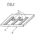
- FIG 2 is a schematic section through a in conjunction with the inventive arrangement usable mask shown.
- the mask (30) exists from a thin membrane (31), for example of silicon oxide, to which the desired Microstructures (32) are applied.
- the microstructures (32) have a different one Material as the membrane (31) so that the microstructures (32) interacting particles experience a different energy loss than those particles, which outside the microstructures (32) have transmitted the mask (30).
Description
Zur teilchenoptischen Erzeugung von Mikrostrukturen, beispielsweise für die Halbleiterlithographie, ist es bekannt, eine verkleinert abzubildende Maske entweder als freitragende Maske oder als dünne Membran mit stark streuenden dickeren Strukturen auszubilden. Bei den freitragenden Masken sind jedoch keine Hohlstrukturen, d.h. Strukturen, die keine Verbindung zum Maskenrand aufweisen, möglich. Da jedoch in der Halbleiterlithographie auch die Projektion derartiger Hohlstrukturen erforderlich ist, ist der Anwendungsbereich freitragender Masken stark begrenzt. Außerdem kommt es durch Teilchenabsorption auf der Maskenstruktur zu einer unterschiedlichen Erwärmung der Maske, woraus leicht ein Maskenverzug resultiert.For the particle-optical generation of microstructures, for example for the Semiconductor lithography, it is known, a reduced-to-be-mapped mask either as self-supporting mask or as a thin membrane with strongly scattering thicker structures train. However, in the cantilevered masks, there are no hollow structures, i. Structures that are not connected to the mask border are possible. However, because in the Semiconductor lithography and the projection of such hollow structures is required, is the Scope of cantilevered masks very limited. It also comes through Particle absorption on the mask structure to a different heating of the Mask, from which easily a mask delay results.
Bei transparenten Masken, bei denen eine stark streuende Struktur auf einer dünnen, schwach streuenden Membran aufgebracht ist, treten diese Nachteile nicht auf Dafür ergibt sich jedoch der Nachteil eines recht geringen Kontrastes, da die Kontrasterzeugung, wie dieses beispielsweise aus der US-A-5079112 bekannt ist, über eine der Maske nachgeschaltete Aperturblende erfolgt, die entweder nur die unter einem großen Streuwinkel aus der Maske austretenden Teilchen transmittieren läßt - dieses entspricht im wesentlichen einem Dunkelfeldkontrast - oder nur die unter kleinen Streuwinkeln aus der Maske austretenden Teilchen transmittieren läßt - dieses entspricht im wesentlichen einem Hellfeldkontrast. Da jedoch sowohl stark als auch schwach streuende Bereiche stets große Streuwinkelbereiche erzeugen, die sich nur in deren statistischer Verteilung unterscheiden, resultiert der bereits oben genannte schwache Kontrast.In the case of transparent masks, where a strongly scattering structure is present on a thin, weakly scattering membrane is applied, these disadvantages do not occur However, the disadvantage of a very low contrast, since the contrast generation, such This is known for example from US-A-5079112, via one of the mask Downstream aperture diaphragm is made, which is either only under a large Scattering angle can be transmitted from the mask emerging particles - this corresponds in essentially a dark field contrast - or only under small scattering angles from the Mask transmits exiting particles - this corresponds essentially to one Bright field contrast. However, since both strong and weakly scattering areas are always large Generate scattering angle ranges that differ only in their statistical distribution, results in the above-mentioned weak contrast.
Es ist daher das Ziel der vorliegenden Erfindung, eine teilchenoptische Anordnung und ein teilchenoptisches Verfahren anzugeben, mit der (dem) auf einer dünnen Membran aufgebrachte Mikrostrukturen mit hohem Kontrast abgebildet werden können. It is therefore the object of the present invention, a particle-optical arrangement and a Specify particle-optical method with which (that) on a thin membrane applied microstructures can be imaged with high contrast.
Dieses Ziel wird durch eine teilchenoptische Anordnung mit den Merkmalen des
Anspruches 1 und durch ein Verfahren mit den Merkmalen des Anspruches 11 gelöst.
Vorteilhafte Ausführungsformen der Erfindung ergeben sich aus den Merkmalen der
abhängigen Ansprüche.This object is achieved by a particle-optical arrangement with the characteristics of
Die erfindungsgemäße teilchenoptische Anordnung weist ein der Mikrostruktur tragenden Maske nachgeschaltetes abbildendes Energiefilter auf Mit Hilfe des Energiefilters werden inelastisch gestreute Teilchen eines vorgegebenen Energiefensters herausgefiltert. Durch ein dem Energiefilter nachgeschaltetes Abbildungssystem erfolgt dann die verkleinerte Abbildung der Maske in die Bild- oder Projektionsebene.The particle-optical arrangement according to the invention has a microstructure-bearing Mask downstream imaging energy filter on Using the energy filter will be Inelastically filtered particles of a given energy window filtered out. By an imaging system downstream of the energy filter then takes the reduced size Illustration of the mask in the image or projection plane.
Der Erfindung liegt demzufolge die Idee zugrunde, für die Kontrasterzeugung eine Trennung der Teilchen nach ihrer Energie bzw. nach ihrem energetischen Unterschied nach Wechselwirkung mit der abzubildenden Maske auszunutzen. Da der Energieverlust der Teilchen stark elementspezifisch ist, läßt sich durch Verwendung unterschiedlicher Materialien für die Membran einerseits und die Mikrostruktur andererseits ein hoher Abbildungskontrast erzeugen. Dabei stört es auch nicht, wenn sowohl die Membran als auch die Mikrostruktur inelastisch streuen, solange sich die Energieverlustspektren der für die Membran und die Mikrostruktur eingesetzten Materialien hinreichend unterscheiden, so daß eine energetische Trennung der inelastisch gestreuten von den inelastisch gestreuten Teilchen am Ausgang des Energiefilters möglich ist. Bevorzugt in Verbindung mit der erfindungsgemäßen Anordnung und dem erfindungsgemäßen Verfahren ist es jedoch, wenn die die Mikrostruktur tragende Maske aus einer die Teilchen elastisch streuenden Trägerfolie mit einer inelastisch streuenden Mikrostruktur besteht. In einem solchen Fall werden vorzugsweise die inelastisch gestreuten Teilchen am Ausgang des Energiefilters herausgefilter, so daß zur Abbildung der Maske nur die elastisch gestreuten Teilchen beitragen, da diese die geringste spektrale Verteilung aufweisen.The invention is therefore based on the idea for the generation of contrast Separation of the particles according to their energy or according to their energetic difference Use interaction with the mask to be imaged. Since the energy loss of Particles strongly element-specific, can be determined by using different Materials for the membrane on the one hand and the microstructure on the other hand, a high Create image contrast. It does not matter if both the membrane as also inelastically scatter the microstructure, as long as the energy loss spectra for the adequately distinguish the materials used in the membrane and the microstructure, so that an energetic separation of the inelastically scattered from the inelastically scattered Particles at the output of the energy filter is possible. Preferably in conjunction with the inventive arrangement and the method according to the invention is, however, if the mask carrying the microstructure consists of one of the particles which spreads elastically Carrier film with an inelastically scattering microstructure. In such a case are preferably the inelastically scattered particles at the output of the energy filter filtered out, so that for imaging the mask only the elastically scattered particles contribute as they have the lowest spectral distribution.
Die Abbildung der Maskenebene in die Bildebene sollte dabei derart erfolgen, daß das Abbild der Maske in der Bildebene höchstens halb so groß ist wie die Maske (Abbildungsmaßstab kleiner 0,5). The image of the mask plane in the image plane should be such that the Image of the mask in the image plane is at most half as large as the mask (Magnification less than 0.5).
Das Energiefilter sollte vorzugsweise als sogenanntes abbildendes Energiefilter ausgebildet sein, das eine erste eingangsseitige Ebene - die Eingangsbildebene - achromatisch in eine erste ausgangsseitige Ebene - Ausgangsbildebene - und eine zweite eingangsseitige Ebene - Eingangsbeugungsebene - dispersiv in eine zweite ausgangsseitige Ebene - dispersive Ebene - abbildet. Die Maske sollte dann entweder in der ersten eingangsseitigen Ebene angeordnet oder durch eine der Maske nachgeschaltete Abbildungsstufe in diese erste eingangsseitige Ebene des Filters abgebildet sein.The energy filter should preferably be designed as a so-called imaging energy filter be that a first input-side plane - the input image plane - achromatisch in one first output-side plane - output image plane - and a second input-side plane - Input diffraction plane - dispersive into a second output-side plane - dispersive Plane - maps. The mask should then be either in the first input-side plane arranged or through a mask downstream of the imaging stage in this first Input side level of the filter to be mapped.
In bzw. hinter der Bildebene der Anordnung ist vorzugsweise ein Präparathalter angeordnet, der zur Aufnahme des zu strukturierenden Wafers dient. Dieser Präparathalter sollte in zwei zueinander senkrechten Richtungen, die senkrecht zur optischen Achse der teilchenoptischen Anordnung stehen, motorisch bewegbar sein. In der Maskenebene sollte ebenfalls ein die Maske aufnehmender, in zwei zueinander senkrechten Richtungen, die wiederum senkrecht zur optischen Achse der teilchenoptischen Anordnung stehen, motorisch bewegbarer Präparathalter angeordnet sein. Durch entsprechende bewegungsmäßige Kopplung des Präparathalters in der Maskenebene mit der Bewegung des Präparathalters in der Bildebene können sukzessiv unterschiedliche Bereiche der Maske auf unterschiedliche Bereiche des in der Bildebene anzuordnenden Wafers energiegefiltert abgebildet werden, so daß durch sukzessive Projektion Maskenfelder abgebildet werden können, die größer als das jeweils übertragene Bildfeld sind.In or behind the image plane of the arrangement is preferably a specimen holder arranged, which serves to receive the wafer to be structured. This specimen holder should be in two mutually perpendicular directions perpendicular to the optical axis of the be particle-optical arrangement, be movable by motor. In the mask level should also a mask receiving, in two mutually perpendicular directions, the again perpendicular to the optical axis of the particle-optical arrangement, be arranged motorically movable specimen holder. By appropriate Movement-like coupling of the specimen holder in the mask plane with the movement of the specimen holder in the image plane can successively different areas of the Mask on different areas of the wafer to be arranged in the image plane imaged in an energy-filtered manner so that mask fields are formed by successive projection can be imaged that are larger than the transmitted image field.
Zwischen Teilchenquelle und der Maskenebene kann ein Kondensorsystem vorgesehen sein. Ein solchen Kondensorsystem ermöglicht es, in der Maskenebene einen kollimierten Strahlengang vorzusehen.Between the particle source and the mask plane, a condenser system may be provided be. Such a condenser system makes it possible to collimate in the mask plane Provide beam path.
Weiterhin kann zwischen der Teilchenquelle und der Maskenebene ein erstes Ablenksystem, zwischen der Maskenebene und dem Energiefilter ein zweites Ablenksystem und hinter dem Energiefilter ein drittes Ablenksystem vorgesehen sein. Jedes dieser drei Ablenksysteme kann dabei in bekannter Weise als Doppelablenksystem ausgebildet sein. Das erste und das zweite Ablenksystem sind dabei vorzugsweise derart erregt, daß ein parallel zur optischen Achse in das erste Ablenksystem eintretender Teilchenstrahl in der Maskenebene auf einen außerachsialen Bereich abgelenkt und hinter der Maskenebene wieder in Richtung auf die optische Achse zurückgelenkt wird. Durch das dritte Ablenksystem hinter dem Energiefilter erfolgt dann wieder eine außerachsiale Auslenkung. Mit der beschriebenen Kombination von Ablenksystemen können unterschiedliche Bereiche der in der Maskenebene anzuordnenden Maske auf unterschiedliche Bereiche auf dem in der Bildebene hinter dem Energiefilter aufzunehmenden Wafer abgebildet werden. Auf diese Weise können elektronenoptisch, d.h. ohne mechanische Bewegung der Maske und des Wafers relativ zueinander sukzessiv größere Maskenbereiche auf den Wafer abgebildet werden. Dabei ist es jedoch besonders vorteilhaft, wenn die teilchenoptische Ablenkung und die mechanische Bewegung des Maskenhalters in der Maskenebene und des Präparathalters in der Bildebene miteinander kombiniert werden, derart daß über eine geeignete Maschinensteuerung jeweils zwischen zwei mechanischen Bewegungen des Maskenhalters in der Maskenebene und des Präparathalters in der Bildebene jeweils zwei oder mehrere teilchenoptisch erzeugte Bildverschiebungen stattfinden.Furthermore, between the particle source and the mask plane a first Deflection system, between the mask layer and the energy filter a second Deflection system and be provided behind the energy filter, a third deflection system. Each of these three deflection systems can in a known manner as Doppelablenksystem be educated. The first and the second deflection system are preferably such excited that a parallel to the optical axis entering the first deflection system Particle beam in the mask plane deflected to an off-axis area and behind the mask plane is directed back towards the optical axis. By the third deflection system behind the energy filter is then again an off-axis Deflection. With the described combination of deflection systems can different areas of the mask to be arranged in the mask mask different areas on the in the image plane behind the energy filter imaged wafers are imaged. In this way, electron-optical, i.e. without mechanical movement of the mask and the wafer successively relative to one another larger mask areas are imaged onto the wafer. But it is special advantageous when the particle-optical deflection and the mechanical movement of the Mask holder in the mask level and the specimen holder in the image plane with each other be combined, so that over a suitable machine control between each two mechanical movements of the mask holder in the mask plane and the Specimen holder in the image plane in each case two or more particle-optically generated Image shifts take place.
Die in Verbindung mit der Erfindung zur Maskenabbildung eingesetzten Teilchen können Elektronen oder Ionen sein, wobei der Einsatz von Elektronen bevorzugt ist, da die für die Erfindung benötigten Komponenten grundsätzlich von Transmissionselektronenmikroskopen bekannt sind.The particles used in conjunction with the invention for mask imaging can Be electrons or ions, wherein the use of electrons is preferred because of the Invention required components in principle of transmission electron microscopes are known.
Nachfolgend werden Einzelheiten der Erfindung anhand der in den Figuren dargestellten Ausführungsbeispiele erläutert.Hereinafter, details of the invention with reference to those shown in the figures Embodiments explained.
Dabei zeigen:
Figur 1- eine vereinfachte Prinzipskizze einer erfindungsgemäßen teilchenoptischen Anordnung;
Figur 2- eine perspektivische Darstellung eines Ausschnitts aus einer in Verbindung mit der Erfindung eingestzten Maske; und
- Figur 3
- die Prinzipskizze eines Ausführungsbeispiels der Erfindung mit teilchenoptischer Bereichsauswahl in der Maskenebene.
- FIG. 1
- a simplified schematic diagram of a particle-optical arrangement according to the invention;
- FIG. 2
- a perspective view of a section of a mask applied in connection with the invention mask; and
- FIG. 3
- the schematic diagram of an embodiment of the invention with particle-optical region selection in the mask layer.
In der Figur 1 ist mit (1) der Crossover einer Teilchenquelle, beispielsweise einer Elektronenquelle, bezeichnet. Ein Kondensor (2) bildet diese Crossoverebene (1) reell in eine Crossoverebene (3) ab. Die Maskenebene (4) befindet sich - in Ausbreitungsrichtung der Teilchen gesehen - hinter der Crossoverebene (3), so daß eine in der Maskenebene (4) angeordnete Maske großflächig und gleichmäßig ausgeleuchtet wird.In FIG. 1, (1) is the crossover of a particle source, for example one Electron source, called. A condenser (2) forms this crossover plane (1) in real a crossover plane (3). The mask plane (4) is located - in the propagation direction of the particles - behind the crossover plane (3), so that one in the mask plane (4) arranged mask is illuminated over a large area and evenly.
Der Maskenebene (4) ist in Strahlrichtung ein Energiefilter (5) nachgeordnet. Dieses Energiefilter ist als sogenanntes abbildendes Energiefilter ausgebildet, das eine erste eingangsseitige Ebene, die Eingangsbildebene, achromatisch in eine erste ausgangsseitige Bildebene, die Ausgangsbildebene, und eine zweite eingangsseitige Ebene, die Eingangsbeugungsebene, dispersiv in eine zweite ausgangsseitige Ebene, die Selektionsebene oder dispersive Ebene abbildet. Derartige Energiefilter sind für Elektronen beispielsweise aus der US-A-4,740,704, US-A- 4,760,261 oder US-A- 5,449,914 bekannt. Auf deren detaillierten Aufbau braucht daher an dieser Stelle nicht näher eingegangen zu werden.The mask plane (4) is arranged downstream of an energy filter (5) in the beam direction. This Energy filter is designed as a so-called imaging energy filter, the first input-side plane, the input image plane, achromatisch in a first output side Image plane, the output image plane, and a second input side plane, the Input diffraction plane, dispersive in a second output-side plane, the Selection level or dispersive plane maps. Such energy filters are for electrons for example, from US-A-4,740,704, US-A-4,760,261 or US-A-5,449,914. Their detailed structure therefore need not be discussed further here become.
Bei der in Figur 1 dargestellten vereinfachten Anordnung fällt die Maskenebene (4) mit der Eingangsbildebene des Filters und die Crossoverebene (3) mit der Eingangsbeugungsebene des Energiefilters zusammen. Demzufolge bildet das Energiefilter (5) die Maskenebene (4) achromatisch in die Ausgangsbildebene (6) und die Crossoverebene (3) achromatisch in die Dispersionsebene (7) ab; der Abbildungsmaßstab sowohl für die Abbildung der Eingangsbildebene als auch für die Abbildung der Eingangsbeugungsebene sollte dabei 1:1 betragen, damit ein weitgehend symmetrischer Verlauf der Teilchenbahnen im Energiefilter gewährleistet ist, wodurch wiederum Abbildungsfehler im Filter vermieden werden. In der Dispersionsebene (7) ist eine Spaltblende angeordnet, durch die Teilchen, die einen vorbestimmten Energieverlust erfahren haben, selektiert werden. Der durch die Spaltblende (7) voreingestellte Energieverlust ist dabei auf den elementspezifischen Energieverlust der Mikrostruktur der in der Maskenebene (4) anzuordnenden Maske einstellbar.In the simplified arrangement shown in Figure 1, the mask plane (4) coincides with the Input image plane of the filter and the crossover plane (3) with the input diffraction plane the energy filter together. As a result, the energy filter (5) forms the mask plane (4) achromatically in the output image plane (6) and the crossover plane (3) achromatically in the Dispersion level (7) from; the magnification for both the image of the Input image plane as well as for the image of the input diffraction plane should be 1: 1, so that a largely symmetrical course of the particle trajectories in Energy filter is ensured, which in turn avoided aberrations in the filter become. In the dispersion plane (7) a slit diaphragm is arranged through which particles, who have experienced a predetermined energy loss can be selected. The one by the Slit diaphragm (7) preset energy loss is on the element-specific Energy loss of the microstructure of the mask to be arranged in the mask plane (4) adjustable.
In Ausbreitungsrichtung der Teilchen gesehen hinter der Spaltblende (7) folgt ein Projektionssystem (8, 9), durch das die Ausgangsbildebene (6) des Energiefilters (5) verkleinert in die Bildebene (10) abgebildet wird. Der Abbildungsmaßstab des Projektionssystems beträgt dabei etwa 0,25, so daß der vom Energiefilter (5) übertragene Bereich der Maskenebene (4) in der Bildebene (10) etwa auf ein Viertel verkleinert erscheint.In the propagation direction of the particles behind the slit diaphragm (7) follows Projection system (8, 9), through which the output image plane (6) of the energy filter (5) zoomed into the image plane (10) is mapped. The magnification of the Projection system is about 0.25, so that of the energy filter (5) transmitted Area of the mask plane (4) in the image plane (10) reduced to about a quarter appears.
Bei dem vereinfachten, in der Figur 1 dargestellten Ausführungsbeispiel ist keine teilchenoptische Auswahl unterschiedlicher Bereiche in der Maskenebene (4) möglich. Um größere Maskenbereiche vollständig in die Bildebene (10) abzubilden, ist hier eine mechanische Relativbewegung sowohl der in der Maskenebene (4) anzuordnenden Maske als auch des in der Bildebene (10) anzuordnenden Wafers erforderlich. Für die entsprechende Bewegung der Maske und des Wafers können die bei elektronenoptischen Inspektionsgeräten eingesetzten Waferstages verwendet werden, die hier in der Figur 1 jedoch nicht dargestellt sind. Die Bewegungen der Waferstages in der Maskenebene (4) und in der Bildebene (10) sind dabei so miteinander zu koppeln, so daß das Verhältnis aus dem Bewegungshub der Maske und dem Bewegungshub des Wafers dem Abbildungsmaßstab zwischen der Maskenebene (4) und der Bildebene (10) entspricht.In the simplified, illustrated in the figure 1 embodiment is no particle-optical selection of different areas in the mask plane (4) possible. Around To image larger mask areas completely in the image plane (10), here is one mechanical relative movement of both in the mask plane (4) to be arranged mask and the wafer to be arranged in the image plane (10). For the corresponding movement of the mask and the wafer can be in the case of electron-optical Waferstages used in inspection equipment used here in the figure 1 but not shown. The movements of the Waferstages in the mask level (4) and in the image plane (10) are to be coupled together so that the ratio of the movement stroke of the mask and the movement stroke of the wafer Mapping scale between the mask layer (4) and the image plane (10) corresponds.
Beim Ausführungsbeispiel in Figur 3 ist die Teilchenquelle mit (11) bezeichnet. Auch hier erzeugt eine erste Kondensorlinse (12) ein reelles Bild (11a) der Quelle (11), einen sogenannten Crossover. In der Crossoverebene ist ein erstes Ablenksystem (13) angeordnet. Dem Ablenksystem (13) folgt eine zweite Kondensorlinse (14) nach, die den Crossover (11a) nach Unendlich abbildet. In Strahlrichtung hinter der zweiten Kondensorlinse (14) im parallelen Strahlengang befindet sich die Maskenebene (15). In der Maskenebene ist der für die Aufnahme der Maske vorgesehene Maskenhalter angeordnet. In the embodiment in Figure 3, the particle source is denoted by (11). Here too A first condenser lens (12) produces a real image (11a) of the source (11) so-called crossover. In the crossover plane is a first deflection system (13) arranged. The deflection system (13) is followed by a second condenser lens (14), which detects the Crossover (11a) maps to infinity. In the beam direction behind the second Condenser lens (14) in the parallel beam path is the mask plane (15). In the Mask level is arranged for receiving the mask mask holder.
Auch bei diesem Ausführungsbeispiel ist der Maskenhalter in zwei zueinander senkrechten Richtungen, die beide senkrecht zur optischen Achse des Abbildungssystems ausgerichtet sind, motorisch bewegbar, um dadurch unterschiedliche Bereiche der aufzunehmenden Maske in den teilchenoptischen Abbildungsstrahlengang zu bringen.Also in this embodiment, the mask holder is in two mutually perpendicular Directions, both aligned perpendicular to the optical axis of the imaging system are, motorically movable to thereby different areas of the male To bring mask into the particle-optical imaging beam path.
Der Maskenebene nach folgt eine dritte Kondensorlinse (16), durch die die Maskenebene (15) in die Eingangsbildebene (18) des Energiefilters (19) abgebildet wird. Die beiden Kondensorlinsen (14, 16) können dabei auch durch eine sogenannte Kondensor- Objektiv-Einfeldlinse realisiert sein.The mask plane is followed by a third condenser lens (16), through which the mask plane (15) is imaged in the input image plane (18) of the energy filter (19). The two Kondensorlinsen (14, 16) can also by a so-called condenser lens Einfeldlinse be realized.
Auch hier handelt es sich bei dem Energiefilter (19) um ein abbildendes Energiefilter, das die Eingangsbildebene (18) achromatisch in die Ausgangsbildebene (20) abbildet und gleichzeitig eine Eingangsbeugungsebene dispersiv in eine ausgangsseitige Selektionsebene (21) abbildet. In der Selektionsebene (21) ist wiederum eine Spaltblende vorgesehen, durch die ein vorgegebener Energieverlust einstellbar ist. Durch ein nachfolgendes Projektionssystem (23, 24) erfolgt wiederum eine verkleinerte Abbildung des in der Ausgangsbildebene (20) des Energiefilters (19) entstehenden Bildes der Maskenebene (15) in die Endbildebene (25).Again, the energy filter (19) is an imaging energy filter that achromatically images the input image plane (18) into the output image plane (20) and simultaneously an input diffraction plane dispersive in an output side Selection level (21) maps. In the selection plane (21) is again a slit diaphragm provided by which a predetermined energy loss is adjustable. Through a Subsequent projection system (23, 24) is again a reduced figure of the image resulting in the output image plane (20) of the energy filter (19) Mask plane (15) in the final image plane (25).
Durch das erste Ablenksystem (13) in der Ebene des Crossovers (11a) vor der Maskenebene (15) kann je nach Erregung des Ablenksystems eine Ablenkung des Teilchenstrahls senkrecht zur optischen Achse erfolgen, so daß je nach Erregung des Ablenksystems (13) unterschiedliche laterale Bereiche (15a, 15b, 15c) in der Maskenebene (15) ausgeleuchtet werden. Der in der Maskenebene (15) telezentrisch außerachsial verlaufende Teilchenstrahl wird durch die dritte Kondensorlinse (16) wieder in Richtung optischer Achse zurückgelenkt. Durch ein zweites Ablenksystem (17), das in der hinteren Brennebene der dritten Kondensorlinse (16) angeordnet ist, erfolgt eine Rücklenkung bzw. Kippung des Teilchenstrahls, die gerade der durch das erste Ablenksystem (13) erzeugten Auslenkung so entgegen gerichtet ist, so daß hinter dem zweiten Ablenksystem (17) die weitere Ausbreitung des Teilchenstrahls unabhängig von der vom ersten Ablenksystem erzeugten Auslenkung ist. Demzufolge ist auch die Ausbreitung des Teilchenstrahls innerhalb des Energiefilters (19) unabhängig von der in der Maskenebene erzielten Strahlauslenkung. Ein drittes Ablenksystem (22), das eine Strahlablenkung um die optische Achse in der Selektionsebene (21) bewirkt, erzeugt wieder eine abschließende Strahlablenkung, die an die Strahlablenkung in der Maskenebene derart angekoppelt ist, daß neben einander liegende Bereiche in der Maskenebene sukzessiv auf neben einander liegende Bereiche in der Bildebene (25) abgebildet werden. Durch diese teilchenoptische Strahlauslenkung können insgesamt größere Feldbereiche in der Maskenebene (15) sukzessiv energiegefiltert in die Bildebene (25) abgebildet werden. Um jedoch noch größere Bildfelder aus der Maskenebene (15) in die Bildebene (25) zu übertragen, sollte auch bei diesem Ausführungsbeispiel der Präparathalter, der das zu strukturierende Präparat, in der Regel den Wafer, in der Bildebene (25) hält, als motorische Waferstage ausgebildet sein, so daß durch entsprechende miteinander gekoppelte Bewegung sowohl der in der Maskenebene (15) aufzunehmenden Maske als auch des in der Bildebene zu haltenden Wafers die gewünschten großen Bildfelder übertragen werden können. Dabei ist es allerdings sinnvoll, zwischen den mechanischen Bewegungen der Maske und des Wafers durch entsprechende Änderungen der Erregungen der Ablenksysteme (13, 17 und 22) durch teilchenoptische Strahlauslenkung jeweils zusammengesetzte größere Teilbildfelder zu erzeugen.By the first deflection system (13) in the plane of the crossover (11a) in front of Masking plane (15) can be a distraction of the depending on the excitation of the deflection system Particle beam perpendicular to the optical axis, so that depending on the excitation of Deflection system (13) different lateral areas (15a, 15b, 15c) in the mask plane (15) are illuminated. The one in the mask plane (15) telecentric off-axis extending particle beam is through the third condenser lens (16) back in the direction deflected back optical axis. By a second deflection system (17), in the rear Focal plane of the third condenser lens (16) is arranged, there is a return or Tilting of the particle beam, just that generated by the first deflection system (13) Deflection is directed so opposite, so that behind the second deflection system (17) the further propagation of the particle beam independent of that of the first deflection system generated deflection is. Consequently, the propagation of the particle beam is also within the energy filter (19) independent of that achieved at the mask level Beam deflection. A third deflection system (22) which deflects the beam around the optical beam Axis in the selection level (21) causes, again produces a final Beam deflection, which is coupled to the beam deflection in the mask plane such that adjacent areas in the mask level successively to each other lying areas in the image plane (25) are mapped. Through this particle-optical Beam deflection can total larger field areas in the mask plane (15) be successively filtered energy filtered in the image plane (25). But still larger fields from the mask layer (15) in the image plane (25) should transfer also in this embodiment of the specimen holder, the structuring the Specimen, usually the wafer, in the image plane (25) holds, as motor wafer days be formed so that by corresponding coupled motion both the mask to be included in the mask plane (15) as well as that in the image plane holding wafers the desired large image fields can be transmitted. It is However, it makes sense between the mechanical movements of the mask and the Wafers by corresponding changes in the excitations of the deflection systems (13, 17 and 22) by particle-optical beam deflection each composed larger To generate partial image fields.
Auch beim Ausführungsbeispiel in der Figur 3 sind die einzelnen teilchenoptischen Komponenten vereinfacht dargestellt. So ist es bei den Ablenksystemen (13, 17, 22) nicht zwingend erforderlich, daß sie in den jeweils genannten Crossoverebenen angeordnet sind. Wichtig ist vielmehr, daß die Ablenksysteme zumindest virtuelle Strahlablenkungen um die Crossoverebenen erzeugen. Soweit die Crossoverebenen aus Platzgründen für ein einfaches Strahlablenksystem nicht zugänglich sind, können die Ablenksysteme in bekannter Weise, wie das Ablenksystem (22) hinter dem Projektionssystem (23, 24), auch als Doppelablenksysteme ausgebildet sein, die lediglich eine virtuelle Kippung in den genannten Crossoverebenen bewirken.Also in the embodiment in Figure 3, the individual particle-optical Simplified components. This is not the case with the deflection systems (13, 17, 22) imperative that they are arranged in each of the said crossover planes. Rather, it is important that the deflection systems at least virtual beam deflections to create the crossover planes. As far as the crossover planes for reasons of space for a simple beam deflection system are not accessible, the deflection systems in known manner, as the deflection system (22) behind the projection system (23, 24), also be designed as Doppelablenksysteme that only a virtual tilt in the cause crossover levels.
Soweit aufgrund der durch die Ablenksysteme erzeugten Ablenkungen die Kondensorlinsen und/oder die Projektivlinsen außeraxial von den Teilchen durchlaufen werden, kann eine Nachfokussierung der betreffenden Linsen sowie eine Änderung der in den Figuren nicht gezeigten Stigmatoren und Justier- und Korrekturelementen in Abhängigkeit von der durch die Ablenksysteme bewirkten Ablenkung erforderlich sein. Die für diese Nachfokussierung und/oder die Änderungen der Stigmatoren und Justier- und Korrekturelemente erforderlichen Strom- und Spannungsänderungen sind als Datentabelle in dem nicht dargestellten Steuerungsrechner abgespeichert, wobei den bewirkten Ablenkungen jeweils die zugehörigen Strom- bzw. Spannungsänderungen zugeordnet sind.Insofar as due to the deflections generated by the deflection systems the Condenser lenses and / or the projectile lenses pass through the particles off-axis may be refocusing of the respective lenses as well as a change in the the figures not shown stigmators and adjustment and correction elements in Depending on the distraction caused by the deflection systems may be required. The for this refocusing and / or the changes of the stigmators and adjusting and Correction elements required current and voltage changes are as a data table stored in the control computer, not shown, causing the Distractions are each associated with the associated current or voltage changes.
In der Figur 2 ist schematisch der Schnitt durch eine in Verbindung mit der erfindungsgemäßen Anordnung einsetzbaren Maske dargestellt. Die Maske (30) besteht aus einer dünnen Membran (31), beispielsweise aus Siliziumoxyd, auf die die gewünschten Mikrostrukturen (32) aufgebracht sind. Die Mikrostrukturen (32) weisen dabei ein anderes Material als die Membran (31) auf, so daß die mit den Mikrostrukturen (32) wechselwirkenden Teilchen einen anderen Energieverlust erfahren als diejenigen Teilchen, die außerhalb der Mikrostrukturen (32) die Maske (30) transmittiert haben.In the figure 2 is a schematic section through a in conjunction with the inventive arrangement usable mask shown. The mask (30) exists from a thin membrane (31), for example of silicon oxide, to which the desired Microstructures (32) are applied. The microstructures (32) have a different one Material as the membrane (31) so that the microstructures (32) interacting particles experience a different energy loss than those particles, which outside the microstructures (32) have transmitted the mask (30).
Durch den erfindungsgemäßen Einsatz einer Energiefilterung bei der Abbildung der Maske ergeben sich gegenüber der bekannten Kontrasterzeugung durch Streuabsorption neben einem höheren Kontrast geringere Farbfehler. Denn da für die Abbildung der Maske in die Bildebene nur ein relativ enger energetischer Bereich der Teilchen ausgenutzt wird, haben die Farbfehler im Abbildungssystem einen geringeren Einfluß. Gleichzeitig wird auch die Energieverbreiterung durch die Wechselwirkung der Teilchen miteinander (Boerscheffekt) reduziert, da aufgrund der Energiefilterung die für die Abbildung nicht genutzten elastisch gestreuten Teilchen eliminiert sind.By the inventive use of an energy filter in the image of the mask arise in comparison to the known contrast generation by litter absorption in addition a higher contrast lower color errors. Because there for the picture of the mask in the Image plane only a relatively narrow energetic range of particles is exploited the color errors in the imaging system have less influence. At the same time, the Energy broadening through the interaction of the particles with each other (Boerscheffekt) reduced because due to the energy filtering the unused for imaging elastic scattered particles are eliminated.
Claims (13)
- Particle-optical arrangement having a mask holder used for holding a mask in a mask plane (4; 15) and an imaging energy filter (5; 19) downstream of the mask holder, wherein the mask plane is imaged at a reduced scale into an image plane (10; 25) by means of the energy filter.
- Particle-optical arrangement according to Claim 1, wherein the imaging energy filter (5; 19) images a first input-side plane (4; 18) achromatically into a first output-side plane (6; 20) and a second input-side plane (3; 17) dispersively into a second output-side plane (7; 21), and wherein the mask plane is arranged in or imaged into the first input-side plane (4; 18).
- Particle-optical arrangement according to Claim 1 or 2, wherein a reduction imaging system (8, 9; 23, 24) is arranged upstream of the energy filter.
- Particle-optical imaging system according to one of Claims 1 - 3, wherein a preparation holder, which can be moved by motors in two mutually perpendicular directions, is arranged in the image plane (10; 25).
- Particle-optical arrangement according to Claim 4, wherein the mask holder can be moved by motors in two mutually perpendicular directions in the mask plane (4; 15) and the movement of the mask holder and the movement of the preparation holder are coupled together.
- Particle-optical imaging system according to one of Claims 1 - 5, wherein a condensor system (2; 12, 14) is provided between the particle source (11) and the mask plane (4; 15).
- Particle-optical imaging system according to one of Claims 1 - 6, wherein a first steering system (13) is provided between the particle source (11) and the mask plane (15), a second steering system (17) is provided between the mask plane and the energy filter (19) and a third steering system (22) is provided downstream of the energy filter.
- Particle-optical imaging system according to Claim 7, wherein the first and second steering systems (13, 17) are actuated so that a particle beam travelling parallel to the optical axis passes through an off-axial region (15a, 15c) in the mask plane (15), is steered back into the direction of the optical axis behind the mask plane (15) and is again steered onto an off-axial region in the image plane (25) behind the energy filter by the third steering system (22).
- Particle-optical imaging system according to Claim 8, wherein the actuation of the condenser lenses (14, 16) and/or other elements, such as stigmators and alignment or correction elements, is changed in the event of a change in the steering caused by the steering systems (13, 17, 20).
- Particle-optical imaging system according to one of Claims 1 - 9, wherein the mask plane (15) lies in a collimated beam path.
- Method for generating microstructures by particle optics, wherein a mask (30) having inelastically scattering microstructures (32) is used and is imaged at a reduced scale onto a wafer by means of an energy filter (5; 19), and wherein particles having a predefined energy loss are selected by using the energy filter (5; 19).
- Method according to Claim 11, wherein the mask consists of a thin support sheet (31) having inelastically scattering microstructures (32).
- Method according to Claim 11 or 12, wherein the support sheet (31) consists of an elastically scattering material.
Applications Claiming Priority (2)
| Application Number | Priority Date | Filing Date | Title |
|---|---|---|---|
| DE19855629 | 1998-12-02 | ||
| DE19855629A DE19855629A1 (en) | 1998-12-02 | 1998-12-02 | Particle-optical arrangement and method for the particle-optical production of microstructures |
Publications (2)
| Publication Number | Publication Date |
|---|---|
| EP1006556A1 EP1006556A1 (en) | 2000-06-07 |
| EP1006556B1 true EP1006556B1 (en) | 2005-08-03 |
Family
ID=7889757
Family Applications (1)
| Application Number | Title | Priority Date | Filing Date |
|---|---|---|---|
| EP99122179A Expired - Lifetime EP1006556B1 (en) | 1998-12-02 | 1999-11-06 | Particle-optical device and method for producing microstructures |
Country Status (6)
| Country | Link |
|---|---|
| US (1) | US6437353B1 (en) |
| EP (1) | EP1006556B1 (en) |
| JP (1) | JP2000173919A (en) |
| DE (2) | DE19855629A1 (en) |
| SG (1) | SG76640A1 (en) |
| TW (1) | TW454220B (en) |
Families Citing this family (10)
| Publication number | Priority date | Publication date | Assignee | Title |
|---|---|---|---|---|
| DE10034412A1 (en) * | 2000-07-14 | 2002-01-24 | Leo Elektronenmikroskopie Gmbh | Process for electron beam lithography and electron optical lithography system |
| DE10053488A1 (en) * | 2000-10-27 | 2002-05-08 | Volkswagen Ag | Processing shredder residues of metal-containing waste comprises producing raw granulate fraction by separating ferromagnetic fraction, non-ferrous metal-containing fraction, granulate fraction and sand fraction |
| DE10053491A1 (en) * | 2000-10-27 | 2002-05-08 | Volkswagen Ag | Processing shredder residues of metal-containing waste comprises producing raw shred fraction by separating ferromagnetic fraction, non-ferrous metal-containing fraction, granulate fraction and sand fraction |
| DE10053487A1 (en) * | 2000-10-27 | 2002-05-08 | Volkswagen Ag | Method for processing shredder residues of metal-containing waste comprises separating the shredder residue into a shredder light fraction and a non-ferromagnetic fraction |
| DE10109965A1 (en) | 2001-03-01 | 2002-09-12 | Zeiss Carl | Particle optical lens arrangement and method using such a lens arrangement |
| DE10117025A1 (en) | 2001-04-05 | 2002-10-10 | Zeiss Carl | Particle optical device, lighting device and projection system and method using the same |
| DE102004037781A1 (en) | 2004-08-03 | 2006-02-23 | Carl Zeiss Nts Gmbh | electron beam device |
| US7504648B2 (en) * | 2007-04-27 | 2009-03-17 | Carestream Health, Inc. | Method and apparatus for determining focus of a scanning system |
| DE102012007868A1 (en) * | 2012-04-19 | 2013-10-24 | Carl Zeiss Microscopy Gmbh | Transmission electron microscopy system |
| CN103777364B (en) * | 2013-12-13 | 2017-10-13 | 北京维信诺科技有限公司 | A kind of manufacture method of graticle |
Family Cites Families (6)
| Publication number | Priority date | Publication date | Assignee | Title |
|---|---|---|---|---|
| DE3532699A1 (en) | 1985-09-13 | 1987-03-26 | Zeiss Carl Fa | ELECTRONIC POWER FILTER OF THE OMEGA TYPE |
| DE3532698A1 (en) | 1985-09-13 | 1987-03-26 | Zeiss Carl Fa | ALPHA TYPE ELECTRONIC POWER FILTER |
| US5079112A (en) * | 1989-08-07 | 1992-01-07 | At&T Bell Laboratories | Device manufacture involving lithographic processing |
| DE4310559A1 (en) | 1993-03-26 | 1994-09-29 | Zeiss Carl Fa | Imaging electron energy filter |
| DE69529987T2 (en) * | 1994-07-15 | 2004-01-15 | Hitachi Ltd | ELECTRONIC ENERGY FILTER |
| US5912469A (en) * | 1996-07-11 | 1999-06-15 | Nikon Corporation | Charged-particle-beam microlithography apparatus |
-
1998
- 1998-12-02 DE DE19855629A patent/DE19855629A1/en not_active Withdrawn
-
1999
- 1999-11-06 DE DE59912355T patent/DE59912355D1/en not_active Expired - Fee Related
- 1999-11-06 EP EP99122179A patent/EP1006556B1/en not_active Expired - Lifetime
- 1999-11-29 TW TW088120776A patent/TW454220B/en not_active IP Right Cessation
- 1999-11-29 SG SG1999005995A patent/SG76640A1/en unknown
- 1999-12-02 US US09/453,991 patent/US6437353B1/en not_active Expired - Fee Related
- 1999-12-02 JP JP11343033A patent/JP2000173919A/en active Pending
Also Published As
| Publication number | Publication date |
|---|---|
| TW454220B (en) | 2001-09-11 |
| DE59912355D1 (en) | 2005-09-08 |
| DE19855629A1 (en) | 2000-06-08 |
| JP2000173919A (en) | 2000-06-23 |
| US6437353B1 (en) | 2002-08-20 |
| SG76640A1 (en) | 2000-11-21 |
| EP1006556A1 (en) | 2000-06-07 |
Similar Documents
| Publication | Publication Date | Title |
|---|---|---|
| EP1835523B1 (en) | Phase-contrast electron microscope | |
| EP0166328B1 (en) | Method of and device for imaging an object or the diffraction diagram of an object through electron energy filtering with a transmission electron microscope | |
| EP2461346B1 (en) | Particle beam apparatus with deflection system | |
| EP1277221B1 (en) | Electron/ion gun for electron or ion beams with high monochromasy or high current density | |
| EP1057204B1 (en) | Device for correcting third-order spherical aberration in a lens, especially the objective lens of an electronic microscope | |
| DE19838600B4 (en) | Energy filter and electron microscope with energy filter | |
| EP0218920A2 (en) | Omega-type electron energy filter | |
| EP0352552B1 (en) | Process for illuminating an object in a transmission electron microscope and electron microscope suitable for that process | |
| DE4129403A1 (en) | IMAGING SYSTEM FOR RADIATION OF CHARGED PARTICLES WITH MIRROR CORRECTOR | |
| DE4310559A1 (en) | Imaging electron energy filter | |
| EP0967630B1 (en) | Electron microscope with imaging magnetic filter | |
| EP1172837B1 (en) | Electron beam lithography method and electron-optical lithography device | |
| EP1006556B1 (en) | Particle-optical device and method for producing microstructures | |
| EP0899771A2 (en) | Energy filter, particularly for electron microscope | |
| DE2512468A1 (en) | ELECTRON MICROSCOPE WITH ENERGY ANALYZER | |
| EP0603555B1 (en) | Method of illumination by focussed electron beam and electron optical illumination system | |
| EP0911860A2 (en) | Particle beam apparatus with energy filter | |
| EP0564438A1 (en) | Particle imaging system, in particular ion optical imaging system | |
| EP2224464A1 (en) | Corpuscular optical image-forming system | |
| DE2742264C3 (en) | Method for imaging an object with low magnification by means of a particle beam device, in particular an electron microscope and particle beam device for carrying out the method | |
| DE10235981B4 (en) | Particle-optical device and electron microscope | |
| DE60037071T2 (en) | Magical energy filter | |
| DE69913313T2 (en) | Quadrupole device for projection lithography using charged particles | |
| DE69913100T2 (en) | PROJECTION LITHOGRAPHY BY CARGO | |
| EP1454334A2 (en) | Lens array with a laterally movable optical axis for corpuscular rays |
Legal Events
| Date | Code | Title | Description |
|---|---|---|---|
| PUAI | Public reference made under article 153(3) epc to a published international application that has entered the european phase |
Free format text: ORIGINAL CODE: 0009012 |
|
| AK | Designated contracting states |
Kind code of ref document: A1 Designated state(s): DE FR GB NL |
|
| AX | Request for extension of the european patent |
Free format text: AL;LT;LV;MK;RO;SI |
|
| RTI1 | Title (correction) |
Free format text: PARTICLE-OPTICAL DEVICE AND METHOD FOR PRODUCING MICROSTRUCTURES |
|
| 17P | Request for examination filed |
Effective date: 20001116 |
|
| AKX | Designation fees paid |
Free format text: DE FR GB NL |
|
| GRAP | Despatch of communication of intention to grant a patent |
Free format text: ORIGINAL CODE: EPIDOSNIGR1 |
|
| RAP1 | Party data changed (applicant data changed or rights of an application transferred) |
Owner name: CARL ZEISS NTS GMBH |
|
| GRAS | Grant fee paid |
Free format text: ORIGINAL CODE: EPIDOSNIGR3 |
|
| GRAA | (expected) grant |
Free format text: ORIGINAL CODE: 0009210 |
|
| AK | Designated contracting states |
Kind code of ref document: B1 Designated state(s): DE FR GB NL |
|
| PG25 | Lapsed in a contracting state [announced via postgrant information from national office to epo] |
Ref country code: NL Free format text: LAPSE BECAUSE OF FAILURE TO SUBMIT A TRANSLATION OF THE DESCRIPTION OR TO PAY THE FEE WITHIN THE PRESCRIBED TIME-LIMIT Effective date: 20050803 Ref country code: GB Free format text: LAPSE BECAUSE OF FAILURE TO SUBMIT A TRANSLATION OF THE DESCRIPTION OR TO PAY THE FEE WITHIN THE PRESCRIBED TIME-LIMIT Effective date: 20050803 |
|
| REG | Reference to a national code |
Ref country code: GB Ref legal event code: FG4D Free format text: NOT ENGLISH |
|
| REF | Corresponds to: |
Ref document number: 59912355 Country of ref document: DE Date of ref document: 20050908 Kind code of ref document: P |
|
| NLV1 | Nl: lapsed or annulled due to failure to fulfill the requirements of art. 29p and 29m of the patents act | ||
| GBV | Gb: ep patent (uk) treated as always having been void in accordance with gb section 77(7)/1977 [no translation filed] |
Effective date: 20050803 |
|
| PLBE | No opposition filed within time limit |
Free format text: ORIGINAL CODE: 0009261 |
|
| STAA | Information on the status of an ep patent application or granted ep patent |
Free format text: STATUS: NO OPPOSITION FILED WITHIN TIME LIMIT |
|
| 26N | No opposition filed |
Effective date: 20060504 |
|
| EN | Fr: translation not filed | ||
| PG25 | Lapsed in a contracting state [announced via postgrant information from national office to epo] |
Ref country code: FR Free format text: LAPSE BECAUSE OF FAILURE TO SUBMIT A TRANSLATION OF THE DESCRIPTION OR TO PAY THE FEE WITHIN THE PRESCRIBED TIME-LIMIT Effective date: 20060929 |
|
| PG25 | Lapsed in a contracting state [announced via postgrant information from national office to epo] |
Ref country code: FR Free format text: LAPSE BECAUSE OF FAILURE TO SUBMIT A TRANSLATION OF THE DESCRIPTION OR TO PAY THE FEE WITHIN THE PRESCRIBED TIME-LIMIT Effective date: 20051130 |
|
| PG25 | Lapsed in a contracting state [announced via postgrant information from national office to epo] |
Ref country code: FR Free format text: LAPSE BECAUSE OF FAILURE TO SUBMIT A TRANSLATION OF THE DESCRIPTION OR TO PAY THE FEE WITHIN THE PRESCRIBED TIME-LIMIT Effective date: 20050803 |
|
| PGFP | Annual fee paid to national office [announced via postgrant information from national office to epo] |
Ref country code: DE Payment date: 20081121 Year of fee payment: 10 |
|
| PG25 | Lapsed in a contracting state [announced via postgrant information from national office to epo] |
Ref country code: DE Free format text: LAPSE BECAUSE OF NON-PAYMENT OF DUE FEES Effective date: 20100601 |