EP0997944A2 - Printed circuit board with integrated circuit devices mounted on both sides thereof - Google Patents
Printed circuit board with integrated circuit devices mounted on both sides thereof Download PDFInfo
- Publication number
- EP0997944A2 EP0997944A2 EP99111996A EP99111996A EP0997944A2 EP 0997944 A2 EP0997944 A2 EP 0997944A2 EP 99111996 A EP99111996 A EP 99111996A EP 99111996 A EP99111996 A EP 99111996A EP 0997944 A2 EP0997944 A2 EP 0997944A2
- Authority
- EP
- European Patent Office
- Prior art keywords
- flat package
- guides
- circuit board
- printed circuit
- edge
- Prior art date
- Legal status (The legal status is an assumption and is not a legal conclusion. Google has not performed a legal analysis and makes no representation as to the accuracy of the status listed.)
- Granted
Links
Images


Classifications
-
- H—ELECTRICITY
- H05—ELECTRIC TECHNIQUES NOT OTHERWISE PROVIDED FOR
- H05K—PRINTED CIRCUITS; CASINGS OR CONSTRUCTIONAL DETAILS OF ELECTRIC APPARATUS; MANUFACTURE OF ASSEMBLAGES OF ELECTRICAL COMPONENTS
- H05K1/00—Printed circuits
- H05K1/18—Printed circuits structurally associated with non-printed electric components
- H05K1/181—Printed circuits structurally associated with non-printed electric components associated with surface mounted components
-
- H—ELECTRICITY
- H01—ELECTRIC ELEMENTS
- H01L—SEMICONDUCTOR DEVICES NOT COVERED BY CLASS H10
- H01L23/00—Details of semiconductor or other solid state devices
- H01L23/02—Containers; Seals
- H01L23/04—Containers; Seals characterised by the shape of the container or parts, e.g. caps, walls
-
- H—ELECTRICITY
- H01—ELECTRIC ELEMENTS
- H01L—SEMICONDUCTOR DEVICES NOT COVERED BY CLASS H10
- H01L23/00—Details of semiconductor or other solid state devices
- H01L23/32—Holders for supporting the complete device in operation, i.e. detachable fixtures
-
- H—ELECTRICITY
- H01—ELECTRIC ELEMENTS
- H01L—SEMICONDUCTOR DEVICES NOT COVERED BY CLASS H10
- H01L23/00—Details of semiconductor or other solid state devices
- H01L23/48—Arrangements for conducting electric current to or from the solid state body in operation, e.g. leads, terminal arrangements ; Selection of materials therefor
- H01L23/488—Arrangements for conducting electric current to or from the solid state body in operation, e.g. leads, terminal arrangements ; Selection of materials therefor consisting of soldered or bonded constructions
- H01L23/495—Lead-frames or other flat leads
- H01L23/49541—Geometry of the lead-frame
- H01L23/49548—Cross section geometry
- H01L23/49551—Cross section geometry characterised by bent parts
- H01L23/49555—Cross section geometry characterised by bent parts the bent parts being the outer leads
-
- H—ELECTRICITY
- H01—ELECTRIC ELEMENTS
- H01L—SEMICONDUCTOR DEVICES NOT COVERED BY CLASS H10
- H01L25/00—Assemblies consisting of a plurality of individual semiconductor or other solid state devices ; Multistep manufacturing processes thereof
- H01L25/03—Assemblies consisting of a plurality of individual semiconductor or other solid state devices ; Multistep manufacturing processes thereof all the devices being of a type provided for in the same subgroup of groups H01L27/00 - H01L33/00, or in a single subclass of H10K, H10N, e.g. assemblies of rectifier diodes
- H01L25/10—Assemblies consisting of a plurality of individual semiconductor or other solid state devices ; Multistep manufacturing processes thereof all the devices being of a type provided for in the same subgroup of groups H01L27/00 - H01L33/00, or in a single subclass of H10K, H10N, e.g. assemblies of rectifier diodes the devices having separate containers
- H01L25/105—Assemblies consisting of a plurality of individual semiconductor or other solid state devices ; Multistep manufacturing processes thereof all the devices being of a type provided for in the same subgroup of groups H01L27/00 - H01L33/00, or in a single subclass of H10K, H10N, e.g. assemblies of rectifier diodes the devices having separate containers the devices being of a type provided for in group H01L27/00
-
- H—ELECTRICITY
- H05—ELECTRIC TECHNIQUES NOT OTHERWISE PROVIDED FOR
- H05K—PRINTED CIRCUITS; CASINGS OR CONSTRUCTIONAL DETAILS OF ELECTRIC APPARATUS; MANUFACTURE OF ASSEMBLAGES OF ELECTRICAL COMPONENTS
- H05K3/00—Apparatus or processes for manufacturing printed circuits
- H05K3/30—Assembling printed circuits with electric components, e.g. with resistor
- H05K3/303—Surface mounted components, e.g. affixing before soldering, aligning means, spacing means
-
- H—ELECTRICITY
- H01—ELECTRIC ELEMENTS
- H01L—SEMICONDUCTOR DEVICES NOT COVERED BY CLASS H10
- H01L2225/00—Details relating to assemblies covered by the group H01L25/00 but not provided for in its subgroups
- H01L2225/03—All the devices being of a type provided for in the same subgroup of groups H01L27/00 - H01L33/648 and H10K99/00
- H01L2225/10—All the devices being of a type provided for in the same subgroup of groups H01L27/00 - H01L33/648 and H10K99/00 the devices having separate containers
- H01L2225/1005—All the devices being of a type provided for in the same subgroup of groups H01L27/00 - H01L33/648 and H10K99/00 the devices having separate containers the devices being of a type provided for in group H01L27/00
- H01L2225/1011—All the devices being of a type provided for in the same subgroup of groups H01L27/00 - H01L33/648 and H10K99/00 the devices having separate containers the devices being of a type provided for in group H01L27/00 the containers being in a stacked arrangement
- H01L2225/1017—All the devices being of a type provided for in the same subgroup of groups H01L27/00 - H01L33/648 and H10K99/00 the devices having separate containers the devices being of a type provided for in group H01L27/00 the containers being in a stacked arrangement the lowermost container comprising a device support
- H01L2225/1029—All the devices being of a type provided for in the same subgroup of groups H01L27/00 - H01L33/648 and H10K99/00 the devices having separate containers the devices being of a type provided for in group H01L27/00 the containers being in a stacked arrangement the lowermost container comprising a device support the support being a lead frame
-
- H—ELECTRICITY
- H01—ELECTRIC ELEMENTS
- H01L—SEMICONDUCTOR DEVICES NOT COVERED BY CLASS H10
- H01L2225/00—Details relating to assemblies covered by the group H01L25/00 but not provided for in its subgroups
- H01L2225/03—All the devices being of a type provided for in the same subgroup of groups H01L27/00 - H01L33/648 and H10K99/00
- H01L2225/10—All the devices being of a type provided for in the same subgroup of groups H01L27/00 - H01L33/648 and H10K99/00 the devices having separate containers
- H01L2225/1005—All the devices being of a type provided for in the same subgroup of groups H01L27/00 - H01L33/648 and H10K99/00 the devices having separate containers the devices being of a type provided for in group H01L27/00
- H01L2225/1011—All the devices being of a type provided for in the same subgroup of groups H01L27/00 - H01L33/648 and H10K99/00 the devices having separate containers the devices being of a type provided for in group H01L27/00 the containers being in a stacked arrangement
- H01L2225/1047—Details of electrical connections between containers
- H01L2225/107—Indirect electrical connections, e.g. via an interposer, a flexible substrate, using TAB
-
- H—ELECTRICITY
- H01—ELECTRIC ELEMENTS
- H01L—SEMICONDUCTOR DEVICES NOT COVERED BY CLASS H10
- H01L2225/00—Details relating to assemblies covered by the group H01L25/00 but not provided for in its subgroups
- H01L2225/03—All the devices being of a type provided for in the same subgroup of groups H01L27/00 - H01L33/648 and H10K99/00
- H01L2225/10—All the devices being of a type provided for in the same subgroup of groups H01L27/00 - H01L33/648 and H10K99/00 the devices having separate containers
- H01L2225/1005—All the devices being of a type provided for in the same subgroup of groups H01L27/00 - H01L33/648 and H10K99/00 the devices having separate containers the devices being of a type provided for in group H01L27/00
- H01L2225/1011—All the devices being of a type provided for in the same subgroup of groups H01L27/00 - H01L33/648 and H10K99/00 the devices having separate containers the devices being of a type provided for in group H01L27/00 the containers being in a stacked arrangement
- H01L2225/1076—Shape of the containers
- H01L2225/1082—Shape of the containers for improving alignment between containers, e.g. interlocking features
-
- H—ELECTRICITY
- H01—ELECTRIC ELEMENTS
- H01L—SEMICONDUCTOR DEVICES NOT COVERED BY CLASS H10
- H01L2924/00—Indexing scheme for arrangements or methods for connecting or disconnecting semiconductor or solid-state bodies as covered by H01L24/00
- H01L2924/0001—Technical content checked by a classifier
- H01L2924/0002—Not covered by any one of groups H01L24/00, H01L24/00 and H01L2224/00
-
- H—ELECTRICITY
- H05—ELECTRIC TECHNIQUES NOT OTHERWISE PROVIDED FOR
- H05K—PRINTED CIRCUITS; CASINGS OR CONSTRUCTIONAL DETAILS OF ELECTRIC APPARATUS; MANUFACTURE OF ASSEMBLAGES OF ELECTRICAL COMPONENTS
- H05K2201/00—Indexing scheme relating to printed circuits covered by H05K1/00
- H05K2201/10—Details of components or other objects attached to or integrated in a printed circuit board
- H05K2201/10431—Details of mounted components
- H05K2201/10439—Position of a single component
- H05K2201/10454—Vertically mounted
-
- H—ELECTRICITY
- H05—ELECTRIC TECHNIQUES NOT OTHERWISE PROVIDED FOR
- H05K—PRINTED CIRCUITS; CASINGS OR CONSTRUCTIONAL DETAILS OF ELECTRIC APPARATUS; MANUFACTURE OF ASSEMBLAGES OF ELECTRICAL COMPONENTS
- H05K2201/00—Indexing scheme relating to printed circuits covered by H05K1/00
- H05K2201/10—Details of components or other objects attached to or integrated in a printed circuit board
- H05K2201/10431—Details of mounted components
- H05K2201/10507—Involving several components
- H05K2201/10545—Related components mounted on both sides of the PCB
-
- H—ELECTRICITY
- H05—ELECTRIC TECHNIQUES NOT OTHERWISE PROVIDED FOR
- H05K—PRINTED CIRCUITS; CASINGS OR CONSTRUCTIONAL DETAILS OF ELECTRIC APPARATUS; MANUFACTURE OF ASSEMBLAGES OF ELECTRICAL COMPONENTS
- H05K2201/00—Indexing scheme relating to printed circuits covered by H05K1/00
- H05K2201/10—Details of components or other objects attached to or integrated in a printed circuit board
- H05K2201/10431—Details of mounted components
- H05K2201/10568—Integral adaptations of a component or an auxiliary PCB for mounting, e.g. integral spacer element
-
- H—ELECTRICITY
- H05—ELECTRIC TECHNIQUES NOT OTHERWISE PROVIDED FOR
- H05K—PRINTED CIRCUITS; CASINGS OR CONSTRUCTIONAL DETAILS OF ELECTRIC APPARATUS; MANUFACTURE OF ASSEMBLAGES OF ELECTRICAL COMPONENTS
- H05K2201/00—Indexing scheme relating to printed circuits covered by H05K1/00
- H05K2201/10—Details of components or other objects attached to or integrated in a printed circuit board
- H05K2201/10613—Details of electrical connections of non-printed components, e.g. special leads
- H05K2201/10621—Components characterised by their electrical contacts
- H05K2201/10659—Different types of terminals for the same component, e.g. solder balls combined with leads
-
- H—ELECTRICITY
- H05—ELECTRIC TECHNIQUES NOT OTHERWISE PROVIDED FOR
- H05K—PRINTED CIRCUITS; CASINGS OR CONSTRUCTIONAL DETAILS OF ELECTRIC APPARATUS; MANUFACTURE OF ASSEMBLAGES OF ELECTRICAL COMPONENTS
- H05K2201/00—Indexing scheme relating to printed circuits covered by H05K1/00
- H05K2201/10—Details of components or other objects attached to or integrated in a printed circuit board
- H05K2201/10613—Details of electrical connections of non-printed components, e.g. special leads
- H05K2201/10621—Components characterised by their electrical contacts
- H05K2201/10696—Single-in-line [SIL] package
-
- H—ELECTRICITY
- H05—ELECTRIC TECHNIQUES NOT OTHERWISE PROVIDED FOR
- H05K—PRINTED CIRCUITS; CASINGS OR CONSTRUCTIONAL DETAILS OF ELECTRIC APPARATUS; MANUFACTURE OF ASSEMBLAGES OF ELECTRICAL COMPONENTS
- H05K2203/00—Indexing scheme relating to apparatus or processes for manufacturing printed circuits covered by H05K3/00
- H05K2203/16—Inspection; Monitoring; Aligning
- H05K2203/167—Using mechanical means for positioning, alignment or registration, e.g. using rod-in-hole alignment
-
- Y—GENERAL TAGGING OF NEW TECHNOLOGICAL DEVELOPMENTS; GENERAL TAGGING OF CROSS-SECTIONAL TECHNOLOGIES SPANNING OVER SEVERAL SECTIONS OF THE IPC; TECHNICAL SUBJECTS COVERED BY FORMER USPC CROSS-REFERENCE ART COLLECTIONS [XRACs] AND DIGESTS
- Y02—TECHNOLOGIES OR APPLICATIONS FOR MITIGATION OR ADAPTATION AGAINST CLIMATE CHANGE
- Y02P—CLIMATE CHANGE MITIGATION TECHNOLOGIES IN THE PRODUCTION OR PROCESSING OF GOODS
- Y02P70/00—Climate change mitigation technologies in the production process for final industrial or consumer products
- Y02P70/50—Manufacturing or production processes characterised by the final manufactured product
Definitions
- This invention relates to semiconductors and, more particularly, to surface-mounted packages for integrated circuit devices.
- Integrated circuit devices have been housed in dual-in-line plastic packages, referred to as DIP packages, for many years in semiconducting manufacturer. These DIP packages have leads extending through holes in a printed circuit board, and the package itself is mounted flat on the board. More recently, surface-mount packaging has been introduced, and this technique eliminates the necessity of soldering leads in holes in the PC boards, so the leads and the PC board connectors can be closer together achieving higher densities.
- edge-mounted packages or modules have been used in an effort to further increase the density of devices, improving cooling and reducing cost.
- U.S. patent 5,260,601 to Baudouin et al. discloses a pair of protruding studs or spacers, positioned on the same edge of a flat package as the leads. These studs or spacers are composed of molded plastic and are formed at the same time as the package itself. The spacers include a reduced-diameter cylindrical portion for insertion into holes in the printed circuit board where the device is to be mounted and include lip or stop portions co-planar with the flat surfaces of the leads so that the leads will be positioned for soldering to the conductors on the printed circuit board.
- the present invention provides an edge-mounted or surface mounted device with respect to the package or the printed circuit board.
- the present invention provides a device that can be packed with a very high packing density and achieves a low profile.
- the high packing density is achieved by packages being positioned on bath sides of the printed circuit board, eliminating the need for two printed circuits boards. Additionally, the layout of the board is simplified because devices mirror each other by rotation.
- the present invention includes a pair of semiconductor integrated semiconductor devices including a first semiconductor integrated circuit device having a first flat package encapsulating a first semiconductor chip, a plurality of first leads extending from one edge of the flat packages, a first guide extending from one edge of the first flat package shaped to fit into a mounting aperture for mechanically positioning and supporting the first flat package when the first conductive leads are soldered in position, a second semiconductor integrated circuit device having an identical or similar second flat package encapsulating a second semiconductor chip, a plurality of second conductive leads extending from one edge of the second flat package, a second guide extending from the one edge of the second flat package that is shaped to fit the aperture for mechanically positioning and supporting the second flat package when the leads are soldered.
- two flat packages 110 in for encapsulating an integrated circuit device (not shown) which is connected to the printed circuit board having a length, a width and a depth by the lead frames 120 by soldered connections 114 through via S to both devices (not shown).
- These lead frames 120 may be connected to bumps on the integrated circuit chip.
- the leads may be connected to bonding pads on the integrated circuit chip.
- the leads are properly aligned by guides in the apertures to provide for connection to the upright flat package 110 which is positioned with respect to the inverted flat package 111 such that a mirrored foot print of the lead frames 120 is obtained.
- connection 114 connects both leadframe 120 of the upright flat package 120 to connection 114 and leadframe 121 of the inverted flat package 111 to connection 114.
- Fig. 2 illustrates one arrangement of guides 100, which achieve the mirrored foot print.
- the guide 100 guides and secures the flat package 110 by wedging the guide 100 against the surface of the mounting aperture 130.
- These guides 100 are of such a length such that the flange 125 is a stop for the guide 100 by abutting the printed circuit board.
- the flange 125 is positioned on guide 100 such that the flange 125 stops the guide 100 in the aperture, preventing the guide 100 from abutting or overlapping with the guide of the opposing flat package 111.
- the flanges 125 are additionally positioned such that the lead frames 120 connect with the connection 125 of the printed circuit board.
- Fig. 6 illustrates that the guides 100 are positioned within the mounting aperture 130 in the printed circuit board and that the flange 125 abuts the printed circuit board, preventing the overlap of the guides in the printed circuit board.
- Fig. 3 illustrates another embodiment of the present invention where the guides may be metal integral with the lead frame.
- the guides of the upright flat package 110 are of a sufficient length to abut and overlap the guides of the inverted flat package 111.
- the guides for example guides 102 and 104 are positioned to be parallel with respect to each other and the length of the flat package yet to be offset such that guide 102 is staggered with respect to guide 104.
- the forward guide 102 of the inverted flat package is in a first plane while the rearward guide 104 of the inverted flat package is in a second plane.
- the first and second planes are substantially parallel for example within 10 degrees of each other.
- forward guide 106 and the rearward guide 108 are similarly parallel offset and staggered with respect to each other.
- This staggered positioning of forward and reverse guides for the inverted and upright flat package respectively achieves the mirrored footprint since any arrangement of the inverted and upright flat packages not achieving the mirrored footprint would result in the distal end of guides 102 and 104 of the inverted mounting package in the mounting aperature 130 abutting the distal end of the guides 106 and 108 of the upright mounting package, preventing the flange 125 from abutting the surface of the printed circuit board and the lead frames 120 from connecting with connections 114.
- the guides 102, 104, 106, 108 securely position the flat packages 110, 111 by wedging the guides 102, 104, 106, 108 against one another and against the surface of the mounting aperature 130 when the mirrored footprint has been achieved.
- Fig. 8 illustrates the guides 102, 104, 106 and 108 within the mounting aperature 130 of the printed circuit board 140. Since the length of each of these guides are greater than one-half the depth of the printed circuit board, the guides overlap and are staggered as illustrated.
- the upright and inverted flat package (Fig. 3) 110 and 111 include flange 125 to stop the guide within the mounting aperture 130.
- the flange 125 is positioned so that the lead frame 120 abuts the connection 114 of the printed circuit board to complete a connection with the printed circuit board. Additionally, the flange 125 when abutting the printed circuit board, positions the guides 102, 104, 106, 108 in the overlapped position.
- Fig. 4 illustrates another embodiment of the present invention.
- the forward guide 202 for the inverted flat package may include an inclined portion 212 to abut an inclined portion 218 of the rearward guide 208 of the upright flat package.
- the forward guide 206 abut of the upright flat package includes an inclined portion 216 to abut an inclined portion 214 of the guide 204 of the rearward flat package.
- the inclined portion 212 facilitates the abutment of the inclined portion 218 to securely wedge the guide against the surface of the mounting aperature.
- the inclined portion 216 facilitates the abutment of the inclined portion 214.
- a plurality of flat packages may be mounted on one side of a printed circuit board 140 and a second plurality of flat packages may be mounted on the opposing side of the printed circuit board 140. This provides for an efficient and high density positioning of the flat packages.
- Fig. 7 illustrates another embodiment of the present invention.
- Fig. 7 illustrates two L-shaped guides in mounting aperature 130.
- L-shaped guide 302 of the upright flat package abuts with the L-shape guide 304 of the inverted flat package.
- Both L-shaped guides 302 and 304 abuts with the surface of the mounting aperature to position and secure the flat package on the printed circuit board.
- Fig. 7 illustrates that guide 302 is smaller than guide 304.
- Fig. 10 illustrates that L-shaped guides 308 are of equal size to L-shaped guides 310.
- the use of the L-shape guides 302 and 304 does not assure that the mirrored footprint is achieved.
- Fig. 9 illustrates another embodiment of the present invention.
- the flat package 110 includes two parallel guides 402 and two perpendicular guides 404.
- the parallel guides 402 are substantially parallel and in the same plane as the length of the flat package 110.
- the perpendicular guides 404 are substantially in the same plane but perpendicular to the length of the flat package.
- Fig. 11 additionally illustrates that the parallel guides 402 of the upright flat package abut the perpendicular guides 406 of the inverted flat package.
- the perpendicular guides 404 of the upright package abut the parallel guide 408 of the inverted flat package. This does achieve the mirrored footprint.
- the above mentioned guides of the present invention may be integrated with the package or lead frame or formed with the flat package after manufacture.
Landscapes
- Engineering & Computer Science (AREA)
- Microelectronics & Electronic Packaging (AREA)
- Physics & Mathematics (AREA)
- Power Engineering (AREA)
- Condensed Matter Physics & Semiconductors (AREA)
- General Physics & Mathematics (AREA)
- Computer Hardware Design (AREA)
- Geometry (AREA)
- Manufacturing & Machinery (AREA)
- Combinations Of Printed Boards (AREA)
- Structures For Mounting Electric Components On Printed Circuit Boards (AREA)
- Lead Frames For Integrated Circuits (AREA)
Abstract
Description
- This invention relates to semiconductors and, more particularly, to surface-mounted packages for integrated circuit devices.
- Integrated circuit devices have been housed in dual-in-line plastic packages, referred to as DIP packages, for many years in semiconducting manufacturer. These DIP packages have leads extending through holes in a printed circuit board, and the package itself is mounted flat on the board. More recently, surface-mount packaging has been introduced, and this technique eliminates the necessity of soldering leads in holes in the PC boards, so the leads and the PC board connectors can be closer together achieving higher densities.
- Similarly, edge-mounted packages or modules have been used in an effort to further increase the density of devices, improving cooling and reducing cost.
- U.S. patent 5,260,601 to Baudouin et al. discloses a pair of protruding studs or spacers, positioned on the same edge of a flat package as the leads. These studs or spacers are composed of molded plastic and are formed at the same time as the package itself. The spacers include a reduced-diameter cylindrical portion for insertion into holes in the printed circuit board where the device is to be mounted and include lip or stop portions co-planar with the flat surfaces of the leads so that the leads will be positioned for soldering to the conductors on the printed circuit board.
- The present invention provides an edge-mounted or surface mounted device with respect to the package or the printed circuit board. The present invention provides a device that can be packed with a very high packing density and achieves a low profile. The high packing density is achieved by packages being positioned on bath sides of the printed circuit board, eliminating the need for two printed circuits boards. Additionally, the layout of the board is simplified because devices mirror each other by rotation.
- The present invention includes a pair of semiconductor integrated semiconductor devices including a first semiconductor integrated circuit device having a first flat package encapsulating a first semiconductor chip, a plurality of first leads extending from one edge of the flat packages, a first guide extending from one edge of the first flat package shaped to fit into a mounting aperture for mechanically positioning and supporting the first flat package when the first conductive leads are soldered in position, a second semiconductor integrated circuit device having an identical or similar second flat package encapsulating a second semiconductor chip, a plurality of second conductive leads extending from one edge of the second flat package, a second guide extending from the one edge of the second flat package that is shaped to fit the aperture for mechanically positioning and supporting the second flat package when the leads are soldered.
- For a more complete understanding of the present invention and for further advantages thereof, references now made to the following detailed description taken in conjunction with the accompanying drawings in which:
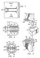
- Fig. 1 illustrates a plan view of a flat package which normally will be vertically surface mounted on edge with guides;
- Fig. 2 illustrates a sectional view of the flat package and a first embodiment of the guides with the printed circuit board;
- Fig. 3 illustrates a perspective view of the flat package with a second embodiment of the guides and an aperture of the printed circuit board;
- Fig. 4 illustrates a top view of the mounting hole of the printed circuit board and guides with split and spring-formed style guides, shaped to allow interlocking guides to provide positive support;
- Fig. 5 illustrates a perspective view of a plurality of flat packages positioned on bath sides of a printed circuit board;
- Fig. 6 illustrates a section view of the first embodiment guides and PC board of the present invention with stud style guides, each extending one-half thickness into PC board;
- Fig. 7 illustrates a top view of a third embodiment of the guides within the mounting hole of the printed circuit board with formed angle style guides, shaped to allow guides to pass from either side of PC board with full thickness extention;
- Fig. 8 illustrates a top view of the guides within the mounting hole with split tab style guides, shaped to allow guides to interlock within PC board mounting hole;
- Fig. 9 illustrates a perspective view of the flat package and a fourth embodiment of guides of the present invention with split tab style guides, oriented to allow interlocking guides within PC board mounting hole;
- Fig. 10 illustrates a top view of additional guides within the mounting hole with formed angle style guides; and
- Fig. 11 illustrates a top view of additional fourth embodiment of guides within the mounting hole.
-
- As illustrated in Fig. 1, two
flat packages 110, in for encapsulating an integrated circuit device (not shown) which is connected to the printed circuit board having a length, a width and a depth by thelead frames 120 by solderedconnections 114 through via S to both devices (not shown). Theselead frames 120 may be connected to bumps on the integrated circuit chip. Alternatively, the leads may be connected to bonding pads on the integrated circuit chip. The leads are properly aligned by guides in the apertures to provide for connection to the uprightflat package 110 which is positioned with respect to the invertedflat package 111 such that a mirrored foot print of thelead frames 120 is obtained. The mirrored footprint is obtained by employing a printed circuit board having the same connection configuration on one side as the other side of the printed circuit board and having the same configuration of the pins in that a particular pin on the uprightflat package 120 is opposite to the same pin on the invertedflat package 121. Fig. 2 further illustrates this aspect of the present invention in thatconnection 114 connects bothleadframe 120 of the uprightflat package 120 toconnection 114 andleadframe 121 of the invertedflat package 111 toconnection 114. - Thus flat packages that may be positioned on the printed circuit board in accordance with this mirrored footprint resulting in a simple and inexpensive printed circuit board.
- Fig. 2 illustrates one arrangement of
guides 100, which achieve the mirrored foot print. Theguide 100 guides and secures theflat package 110 by wedging theguide 100 against the surface of themounting aperture 130. Theseguides 100 are of such a length such that theflange 125 is a stop for theguide 100 by abutting the printed circuit board. Theflange 125 is positioned onguide 100 such that theflange 125 stops theguide 100 in the aperture, preventing theguide 100 from abutting or overlapping with the guide of the opposingflat package 111. Theflanges 125 are additionally positioned such that thelead frames 120 connect with theconnection 125 of the printed circuit board. - Fig. 6 illustrates that the
guides 100 are positioned within themounting aperture 130 in the printed circuit board and that theflange 125 abuts the printed circuit board, preventing the overlap of the guides in the printed circuit board. - Fig. 3 illustrates another embodiment of the present invention where the guides may be metal integral with the lead frame. In this embodiment, the guides of the upright
flat package 110 are of a sufficient length to abut and overlap the guides of the invertedflat package 111. The guides forexample guides guide 102 is staggered with respect toguide 104. For example, theforward guide 102 of the inverted flat package is in a first plane while therearward guide 104 of the inverted flat package is in a second plane. The first and second planes are substantially parallel for example within 10 degrees of each other. Additionally, theforward guide 106 and therearward guide 108 are similarly parallel offset and staggered with respect to each other. This staggered positioning of forward and reverse guides for the inverted and upright flat package respectively achieves the mirrored footprint since any arrangement of the inverted and upright flat packages not achieving the mirrored footprint would result in the distal end ofguides mounting aperature 130 abutting the distal end of theguides flange 125 from abutting the surface of the printed circuit board and thelead frames 120 from connecting withconnections 114. Theguides flat packages guides mounting aperature 130 when the mirrored footprint has been achieved. - Fig. 8 illustrates the
guides mounting aperature 130 of the printedcircuit board 140. Since the length of each of these guides are greater than one-half the depth of the printed circuit board, the guides overlap and are staggered as illustrated. - The upright and inverted flat package (Fig. 3) 110 and 111 include
flange 125 to stop the guide within themounting aperture 130. Theflange 125 is positioned so that thelead frame 120 abuts theconnection 114 of the printed circuit board to complete a connection with the printed circuit board. Additionally, theflange 125 when abutting the printed circuit board, positions theguides - Fig. 4 illustrates another embodiment of the present invention. The
forward guide 202 for the inverted flat package may include aninclined portion 212 to abut aninclined portion 218 of therearward guide 208 of the upright flat package. Likewise, theforward guide 206 abut of the upright flat package includes aninclined portion 216 to abut aninclined portion 214 of theguide 204 of the rearward flat package. Theinclined portion 212 facilitates the abutment of theinclined portion 218 to securely wedge the guide against the surface of the mounting aperature. Theinclined portion 216 facilitates the abutment of theinclined portion 214. - As illustrated in Fig. 5, a plurality of flat packages may be mounted on one side of a printed
circuit board 140 and a second plurality of flat packages may be mounted on the opposing side of the printedcircuit board 140. This provides for an efficient and high density positioning of the flat packages. - Fig. 7 illustrates another embodiment of the present invention. Fig. 7 illustrates two L-shaped guides in
mounting aperature 130. L-shapedguide 302 of the upright flat package abuts with the L-shape guide 304 of the inverted flat package. Both L-shapedguides guide 302 is smaller thanguide 304. - Fig. 10 illustrates that L-shaped
guides 308 are of equal size to L-shapedguides 310. The use of the L-shape guides 302 and 304 does not assure that the mirrored footprint is achieved. - Fig. 9 illustrates another embodiment of the present invention. The
flat package 110 includes twoparallel guides 402 and twoperpendicular guides 404. The parallel guides 402 are substantially parallel and in the same plane as the length of theflat package 110. Furthermore, the perpendicular guides 404 are substantially in the same plane but perpendicular to the length of the flat package. Fig. 11 additionally illustrates that theparallel guides 402 of the upright flat package abut the perpendicular guides 406 of the inverted flat package. Additionally, the perpendicular guides 404 of the upright package abut theparallel guide 408 of the inverted flat package. This does achieve the mirrored footprint. - The above mentioned guides of the present invention may be integrated with the package or lead frame or formed with the flat package after manufacture.
- Although the present invention and its advantages have been described in detail, it should be understood that various changes, substitutions and alterations can be made herein without departing from the spirit and scope of the invention as defined by the appended claims.
Claims (2)
- A surface mounted integrated circuit structure comprising:a printed circuit board having a surface, the surface having mounting apertures, a first semiconductor integrated circuit device having a first flat package encapsulating a first semiconductor chip, a plurality of first conductive leads extending from one edge of said first flat package, first guides extending from the said one edge of said first flat package and shaped to fit into said apertures of said printed circuit board for mechanically positioning and supporting said first flat package when the first conductive leads are soldered to said printed circuit board; anda second integrated circuit device having a second flat package encapsulating a second semiconductor chip, a plurality of second conductive leads extending from one edge of said second flat package, second guides extending from the said one edge of the second flat package and shaped to fit into said same apertures as said first guides for mechanically positioning and supporting the package when said second conductive leads are soldered to said printed circuit board,
wherein said first and second guides are positioned in said mounting apertures such that said first conductive leads form a mirrored footprint with respect to said second conductive leads. - A pair of semiconductor integrated circuit devices comprising:a first semiconductor integrated circuit device having a first flat package encapsulating a first semiconductor ship, a plurality of first conductive leads extending from one edge of said first flat package, a first guide extending from said one edge of said first flat package shaped to fit into an aperture for mechanically positioning and supporting said first flat package when said first conductive leads are soldered in position; anda second semiconductor integrated circuit device having a second flat package encapsulating a second semiconductor chip, a plurality of second conductive leads extending from one edge of the second flat package, a second guide extending from said one edge of said second flat package that are shaped to fit in said same aperture as the first guide for mechanically positioning and supporting said second flat package when the leads are soldered,
wherein said first and second guides are positioned in said aperture such that said first conductive leads form a mirrored footprint with respect to said second conductive leads.
Applications Claiming Priority (3)
| Application Number | Priority Date | Filing Date | Title |
|---|---|---|---|
| US24182494A | 1994-05-12 | 1994-05-12 | |
| US241824 | 1994-05-12 | ||
| EP95107226A EP0682366A3 (en) | 1994-05-12 | 1995-05-12 | Mounting of integrated circuit devices. |
Related Parent Applications (1)
| Application Number | Title | Priority Date | Filing Date |
|---|---|---|---|
| EP95107226A Division EP0682366A3 (en) | 1994-05-12 | 1995-05-12 | Mounting of integrated circuit devices. |
Publications (3)
| Publication Number | Publication Date |
|---|---|
| EP0997944A2 true EP0997944A2 (en) | 2000-05-03 |
| EP0997944A3 EP0997944A3 (en) | 2000-05-10 |
| EP0997944B1 EP0997944B1 (en) | 2003-10-29 |
Family
ID=22912330
Family Applications (2)
| Application Number | Title | Priority Date | Filing Date |
|---|---|---|---|
| EP95107226A Withdrawn EP0682366A3 (en) | 1994-05-12 | 1995-05-12 | Mounting of integrated circuit devices. |
| EP99111996A Expired - Lifetime EP0997944B1 (en) | 1994-05-12 | 1995-05-12 | Printed circuit board with integrated circuit devices mounted on both sides thereof |
Family Applications Before (1)
| Application Number | Title | Priority Date | Filing Date |
|---|---|---|---|
| EP95107226A Withdrawn EP0682366A3 (en) | 1994-05-12 | 1995-05-12 | Mounting of integrated circuit devices. |
Country Status (6)
| Country | Link |
|---|---|
| US (1) | US5671125A (en) |
| EP (2) | EP0682366A3 (en) |
| JP (1) | JPH0864921A (en) |
| KR (1) | KR950034708A (en) |
| DE (1) | DE69532050T2 (en) |
| TW (1) | TW340256B (en) |
Families Citing this family (13)
| Publication number | Priority date | Publication date | Assignee | Title |
|---|---|---|---|---|
| US6135781A (en) * | 1996-07-17 | 2000-10-24 | Minnesota Mining And Manufacturing Company | Electrical interconnection system and device |
| KR100268460B1 (en) * | 1996-12-07 | 2000-10-16 | 윤종용 | Positioning device of surface mount semiconductor IC |
| US6163459A (en) * | 1997-07-25 | 2000-12-19 | Matsushita Electric Industrial Co., Ltd. | Semiconductor mounting system and semiconductor chip |
| CN1113588C (en) | 1997-08-08 | 2003-07-02 | 诺基亚网络有限公司 | Method of manufacturing surface-mountable SIL hybrid circuit |
| DE19740701C2 (en) * | 1997-09-16 | 1999-08-19 | Siemens Ag | Semiconductor component arrangement with a component having an auxiliary element in VSMP design |
| DE19846456A1 (en) * | 1998-10-08 | 2000-01-27 | Siemens Ag | Electronic component with semiconductor component and lead frame |
| US6483041B1 (en) * | 1999-11-12 | 2002-11-19 | Emc Corporation | Micro soldered connection |
| US6409538B1 (en) * | 2000-11-03 | 2002-06-25 | Cray Inc. | Electrical connector assembly for use with variable thickness circuit boards |
| US6552275B2 (en) * | 2001-04-16 | 2003-04-22 | Intel Corporation | Surface mount component |
| JP2005181222A (en) * | 2003-12-22 | 2005-07-07 | Renesas Technology Corp | Manufacturing method for semiconductor device |
| US20060084318A1 (en) * | 2004-10-18 | 2006-04-20 | Jason Si | Double-side mounting electrical connector |
| CN101151356B (en) * | 2005-10-28 | 2013-01-23 | 深圳芯邦科技股份有限公司 | Making method of storage device with compatible collocation functional control chip |
| WO2008069755A1 (en) * | 2006-12-05 | 2008-06-12 | Infineon Technologies Ag | Integrated semiconductor outline package |
Citations (5)
| Publication number | Priority date | Publication date | Assignee | Title |
|---|---|---|---|---|
| US4994896A (en) * | 1987-05-27 | 1991-02-19 | Mitsubishi Denki Kabushiki Kaisha | Semiconductor device |
| EP0427151A2 (en) * | 1989-11-06 | 1991-05-15 | Micron Technology, Inc. | Gull-wing zig-zag inline-lead package having end-of-package anchoring pins |
| US5061990A (en) * | 1987-09-21 | 1991-10-29 | Hitachi Maxell, Ltd. | Semiconductor device and the manufacture thereof |
| EP0527044A1 (en) * | 1991-08-05 | 1993-02-10 | International Business Machines Corporation | Memory package |
| US5260601A (en) * | 1988-03-14 | 1993-11-09 | Texas Instruments Incorporated | Edge-mounted, surface-mount package for semiconductor integrated circuit devices |
Family Cites Families (13)
| Publication number | Priority date | Publication date | Assignee | Title |
|---|---|---|---|---|
| US4546406A (en) * | 1980-09-25 | 1985-10-08 | Texas Instruments Incorporated | Electronic circuit interconnection system |
| US4750089A (en) * | 1985-11-22 | 1988-06-07 | Texas Instruments Incorporated | Circuit board with a chip carrier and mounting structure connected to the chip carrier |
| US4974057A (en) * | 1986-10-31 | 1990-11-27 | Texas Instruments Incorporated | Semiconductor device package with circuit board and resin |
| US4979015A (en) * | 1987-01-28 | 1990-12-18 | Texas Instruments Incorporated | Insulated substrate for flip-chip integrated circuit device |
| EP0282617A1 (en) * | 1987-03-18 | 1988-09-21 | Texas Instruments Deutschland Gmbh | Integrated circuit having an electroconductive mounting |
| US4855809A (en) * | 1987-11-24 | 1989-08-08 | Texas Instruments Incorporated | Orthogonal chip mount system module and method |
| US4963697A (en) * | 1988-02-12 | 1990-10-16 | Texas Instruments Incorporated | Advanced polymers on metal printed wiring board |
| US4975763A (en) * | 1988-03-14 | 1990-12-04 | Texas Instruments Incorporated | Edge-mounted, surface-mount package for semiconductor integrated circuit devices |
| US4967042A (en) * | 1988-12-22 | 1990-10-30 | Texas Instruments Incorporated | System for enhancing current carrying capacity of printed wiring board |
| US5059557A (en) * | 1989-08-08 | 1991-10-22 | Texas Instruments Incorporated | Method of electrically connecting integrated circuits by edge-insertion in grooved support members |
| US5080611A (en) * | 1990-12-21 | 1992-01-14 | Amp Incorporated | Boardlock for common-hole double-sided mounting |
| US5352851A (en) * | 1992-09-08 | 1994-10-04 | Texas Instruments Incorporated | Edge-mounted, surface-mount integrated circuit device |
| KR950014123B1 (en) * | 1992-09-08 | 1995-11-21 | 삼성전자주식회사 | Semiconductor package |
-
1995
- 1995-05-12 JP JP7158249A patent/JPH0864921A/en active Pending
- 1995-05-12 EP EP95107226A patent/EP0682366A3/en not_active Withdrawn
- 1995-05-12 EP EP99111996A patent/EP0997944B1/en not_active Expired - Lifetime
- 1995-05-12 DE DE69532050T patent/DE69532050T2/en not_active Expired - Fee Related
- 1995-05-12 KR KR1019950011681A patent/KR950034708A/en not_active Application Discontinuation
- 1995-06-19 TW TW084106253A patent/TW340256B/en not_active IP Right Cessation
- 1995-08-21 US US08/517,308 patent/US5671125A/en not_active Expired - Lifetime
Patent Citations (5)
| Publication number | Priority date | Publication date | Assignee | Title |
|---|---|---|---|---|
| US4994896A (en) * | 1987-05-27 | 1991-02-19 | Mitsubishi Denki Kabushiki Kaisha | Semiconductor device |
| US5061990A (en) * | 1987-09-21 | 1991-10-29 | Hitachi Maxell, Ltd. | Semiconductor device and the manufacture thereof |
| US5260601A (en) * | 1988-03-14 | 1993-11-09 | Texas Instruments Incorporated | Edge-mounted, surface-mount package for semiconductor integrated circuit devices |
| EP0427151A2 (en) * | 1989-11-06 | 1991-05-15 | Micron Technology, Inc. | Gull-wing zig-zag inline-lead package having end-of-package anchoring pins |
| EP0527044A1 (en) * | 1991-08-05 | 1993-02-10 | International Business Machines Corporation | Memory package |
Also Published As
| Publication number | Publication date |
|---|---|
| TW340256B (en) | 1998-09-11 |
| DE69532050T2 (en) | 2004-08-26 |
| KR950034708A (en) | 1995-12-28 |
| EP0997944A3 (en) | 2000-05-10 |
| EP0997944B1 (en) | 2003-10-29 |
| US5671125A (en) | 1997-09-23 |
| JPH0864921A (en) | 1996-03-08 |
| EP0682366A2 (en) | 1995-11-15 |
| DE69532050D1 (en) | 2003-12-04 |
| EP0682366A3 (en) | 1996-03-06 |
Similar Documents
| Publication | Publication Date | Title |
|---|---|---|
| KR0127873B1 (en) | Edge-mounted surface-mount package for semiconductor integrated circuit device in tergrateles | |
| US5600178A (en) | Semiconductor package having interdigitated leads | |
| KR0153595B1 (en) | Semiconductor device manufacture and semiconductor module thereof | |
| US5671125A (en) | Vertical package mounted on both sides of a printed circuit board | |
| US5260601A (en) | Edge-mounted, surface-mount package for semiconductor integrated circuit devices | |
| JP2538107B2 (en) | Method for manufacturing high density semiconductor module | |
| JPH09172134A (en) | Electronic package assembly and electronic module | |
| JPH0354435B2 (en) | ||
| JP2747634B2 (en) | Surface mount type diode | |
| US5781415A (en) | Semiconductor package and mounting method | |
| US5432678A (en) | High power dissipation vertical mounted package for surface mount application | |
| US5728601A (en) | Process for manufacturing a single in-line package for surface mounting | |
| JPH04167457A (en) | Semiconductor device | |
| US4989066A (en) | Semiconductor package | |
| JP2805471B2 (en) | Manufacturing method of surface mount type diode | |
| JPS62262447A (en) | Semiconductor package and mounting thereof | |
| JPH01220837A (en) | Semiconductor integrated circuit device | |
| JP2766401B2 (en) | Surface mount type semiconductor device | |
| JPH07147368A (en) | Semiconductor integrated circuit device and its mounting structure | |
| KR100239687B1 (en) | Ultra-thin memory module | |
| KR0142841B1 (en) | Staiu package and the method | |
| KR0122951Y1 (en) | Printed circuit board structure of double faced forms terminal | |
| JPH06112343A (en) | Semiconductor device | |
| JPH09116080A (en) | Lead terminal and lead frame to be used for it | |
| JPH0239484A (en) | Printed circuit board |
Legal Events
| Date | Code | Title | Description |
|---|---|---|---|
| PUAI | Public reference made under article 153(3) epc to a published international application that has entered the european phase |
Free format text: ORIGINAL CODE: 0009012 |
|
| PUAL | Search report despatched |
Free format text: ORIGINAL CODE: 0009013 |
|
| AC | Divisional application: reference to earlier application |
Ref document number: 682366 Country of ref document: EP |
|
| AK | Designated contracting states |
Kind code of ref document: A2 Designated state(s): DE FR GB IT NL |
|
| AK | Designated contracting states |
Kind code of ref document: A3 Designated state(s): DE FR GB IT NL |
|
| 17P | Request for examination filed |
Effective date: 20001110 |
|
| 17Q | First examination report despatched |
Effective date: 20010504 |
|
| GRAH | Despatch of communication of intention to grant a patent |
Free format text: ORIGINAL CODE: EPIDOS IGRA |
|
| GRAS | Grant fee paid |
Free format text: ORIGINAL CODE: EPIDOSNIGR3 |
|
| GRAA | (expected) grant |
Free format text: ORIGINAL CODE: 0009210 |
|
| AC | Divisional application: reference to earlier application |
Ref document number: 0682366 Country of ref document: EP Kind code of ref document: P |
|
| AK | Designated contracting states |
Kind code of ref document: B1 Designated state(s): DE FR GB IT NL |
|
| PG25 | Lapsed in a contracting state [announced via postgrant information from national office to epo] |
Ref country code: NL Free format text: LAPSE BECAUSE OF FAILURE TO SUBMIT A TRANSLATION OF THE DESCRIPTION OR TO PAY THE FEE WITHIN THE PRESCRIBED TIME-LIMIT Effective date: 20031029 Ref country code: IT Free format text: LAPSE BECAUSE OF FAILURE TO SUBMIT A TRANSLATION OF THE DESCRIPTION OR TO PAY THE FEE WITHIN THE PRESCRIBED TIME-LIMIT;WARNING: LAPSES OF ITALIAN PATENTS WITH EFFECTIVE DATE BEFORE 2007 MAY HAVE OCCURRED AT ANY TIME BEFORE 2007. THE CORRECT EFFECTIVE DATE MAY BE DIFFERENT FROM THE ONE RECORDED. Effective date: 20031029 |
|
| REG | Reference to a national code |
Ref country code: GB Ref legal event code: FG4D |
|
| REF | Corresponds to: |
Ref document number: 69532050 Country of ref document: DE Date of ref document: 20031204 Kind code of ref document: P |
|
| NLV1 | Nl: lapsed or annulled due to failure to fulfill the requirements of art. 29p and 29m of the patents act | ||
| ET | Fr: translation filed | ||
| PLBE | No opposition filed within time limit |
Free format text: ORIGINAL CODE: 0009261 |
|
| STAA | Information on the status of an ep patent application or granted ep patent |
Free format text: STATUS: NO OPPOSITION FILED WITHIN TIME LIMIT |
|
| 26N | No opposition filed |
Effective date: 20040730 |
|
| PGFP | Annual fee paid to national office [announced via postgrant information from national office to epo] |
Ref country code: FR Payment date: 20090507 Year of fee payment: 15 Ref country code: DE Payment date: 20090529 Year of fee payment: 15 |
|
| PGFP | Annual fee paid to national office [announced via postgrant information from national office to epo] |
Ref country code: GB Payment date: 20090407 Year of fee payment: 15 |
|
| GBPC | Gb: european patent ceased through non-payment of renewal fee |
Effective date: 20100512 |
|
| REG | Reference to a national code |
Ref country code: FR Ref legal event code: ST Effective date: 20110131 |
|
| PG25 | Lapsed in a contracting state [announced via postgrant information from national office to epo] |
Ref country code: DE Free format text: LAPSE BECAUSE OF NON-PAYMENT OF DUE FEES Effective date: 20101201 |
|
| PG25 | Lapsed in a contracting state [announced via postgrant information from national office to epo] |
Ref country code: FR Free format text: LAPSE BECAUSE OF NON-PAYMENT OF DUE FEES Effective date: 20100531 |
|
| PG25 | Lapsed in a contracting state [announced via postgrant information from national office to epo] |
Ref country code: GB Free format text: LAPSE BECAUSE OF NON-PAYMENT OF DUE FEES Effective date: 20100512 |