EP0997737B1 - Semiconductor acceleration sensor and self-diagnosis thereof - Google Patents
Semiconductor acceleration sensor and self-diagnosis thereof Download PDFInfo
- Publication number
- EP0997737B1 EP0997737B1 EP99905235A EP99905235A EP0997737B1 EP 0997737 B1 EP0997737 B1 EP 0997737B1 EP 99905235 A EP99905235 A EP 99905235A EP 99905235 A EP99905235 A EP 99905235A EP 0997737 B1 EP0997737 B1 EP 0997737B1
- Authority
- EP
- European Patent Office
- Prior art keywords
- acceleration sensor
- outside
- section
- central
- semiconductor acceleration
- Prior art date
- Legal status (The legal status is an assumption and is not a legal conclusion. Google has not performed a legal analysis and makes no representation as to the accuracy of the status listed.)
- Expired - Lifetime
Links
Images


Classifications
-
- H—ELECTRICITY
- H01—ELECTRIC ELEMENTS
- H01H—ELECTRIC SWITCHES; RELAYS; SELECTORS; EMERGENCY PROTECTIVE DEVICES
- H01H35/00—Switches operated by change of a physical condition
- H01H35/14—Switches operated by change of acceleration, e.g. by shock or vibration, inertia switch
- H01H35/141—Details
- H01H35/142—Damping means to avoid unwanted response
-
- G—PHYSICS
- G01—MEASURING; TESTING
- G01P—MEASURING LINEAR OR ANGULAR SPEED, ACCELERATION, DECELERATION, OR SHOCK; INDICATING PRESENCE, ABSENCE, OR DIRECTION, OF MOVEMENT
- G01P15/00—Measuring acceleration; Measuring deceleration; Measuring shock, i.e. sudden change of acceleration
- G01P15/02—Measuring acceleration; Measuring deceleration; Measuring shock, i.e. sudden change of acceleration by making use of inertia forces using solid seismic masses
- G01P15/08—Measuring acceleration; Measuring deceleration; Measuring shock, i.e. sudden change of acceleration by making use of inertia forces using solid seismic masses with conversion into electric or magnetic values
- G01P15/0802—Details
-
- G—PHYSICS
- G01—MEASURING; TESTING
- G01P—MEASURING LINEAR OR ANGULAR SPEED, ACCELERATION, DECELERATION, OR SHOCK; INDICATING PRESENCE, ABSENCE, OR DIRECTION, OF MOVEMENT
- G01P15/00—Measuring acceleration; Measuring deceleration; Measuring shock, i.e. sudden change of acceleration
- G01P15/02—Measuring acceleration; Measuring deceleration; Measuring shock, i.e. sudden change of acceleration by making use of inertia forces using solid seismic masses
- G01P15/08—Measuring acceleration; Measuring deceleration; Measuring shock, i.e. sudden change of acceleration by making use of inertia forces using solid seismic masses with conversion into electric or magnetic values
- G01P15/135—Measuring acceleration; Measuring deceleration; Measuring shock, i.e. sudden change of acceleration by making use of inertia forces using solid seismic masses with conversion into electric or magnetic values by making use of contacts which are actuated by a movable inertial mass
-
- H—ELECTRICITY
- H01—ELECTRIC ELEMENTS
- H01H—ELECTRIC SWITCHES; RELAYS; SELECTORS; EMERGENCY PROTECTIVE DEVICES
- H01H1/00—Contacts
- H01H1/0015—Means for testing or for inspecting contacts, e.g. wear indicator
-
- H—ELECTRICITY
- H01—ELECTRIC ELEMENTS
- H01H—ELECTRIC SWITCHES; RELAYS; SELECTORS; EMERGENCY PROTECTIVE DEVICES
- H01H1/00—Contacts
- H01H1/0036—Switches making use of microelectromechanical systems [MEMS]
Definitions
- the present invention relates to a semiconductor acceleration sensor according to the preamble of claim 1 and a semiconductor acceleration self-diagnosing method.
- Such a semiconductor acceleration sensor is already known from JP 09 269 336 A.
- Said document discloses a silicon substrate, a beam and a moving mass. At least one moving contact is installed at the moving mass which is supported by the beam. A fixed contact is installed so as to face the moving contact. The center of gravity of the moving mass is arranged on the central axis of the beam. The thickness and the width of the moving mass are set at values which are sufficiently larger than those of the beam. An electrode for self-diagnosis and an electrode for pre-bias are arranged so as to face the moving mass.
- An example of a conventional acceleration sensor employs a ball (like an iron ball). In the sensor, when an acceleration greater than a predetermined value is applied to the sensor, the ball is moved to operate a switch.
- a mercury switch is employed (cf. Japanese Utility Patent Application (OPI) No. 136565/1992 and 127574 (the term “OPI” as used herein means an "unexamined published application”).
- Those conventional sensors are bulky, and are made up of a number of components, and therefore it is necessary to determined a particular position to install them, and they are high in manufacturing cost.
- An object of the invention is to provide a semiconductor acceleration sensor which is small in size, light in weight, simple in manufacture, low in manufacturing cost, and high in accuracy, and which, with a switch-on time set to a predetermined value, is stable in operation.
- a further object of the invention is to provide a semiconductor acceleration sensor self-diagnosing method which diagnoses the semiconductor acceleration sensor.
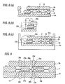
- FIG. 1 is an explanatory diagram of an example of a semiconductor acceleration sensor, which constitutes a first embodiment of the invention.
- FIG. 2 is an explanatory diagram for a description of the semiconductor acceleration sensor shown in FIG. 1.
- FIG. 3 is an explanatory diagram for a description of the semiconductor acceleration sensor shown in FIG. 1.
- FIG. 4 is an explanatory diagram for a description of a both-direction operation of the semiconductor acceleration sensor shown in FIG. 1.
- FIG. 5 is an explanatory diagram for a description of the manufacturing steps of the central board of the semiconductor acceleration sensor shown in FIG. 1.
- FIG. 6 is an explanatory diagram for a description of the manufacturing steps of the central board (or the first layer) of the semiconductor acceleration sensor shown in FIG. 1.
- FIG. 7 is an explanatory diagram for a description of the manufacturing steps of the outside board (or the third layer) of the semiconductor acceleration sensor shown in FIG. 1.
- FIG. 8 is an explanatory diagram for a description of the assembling steps of the semiconductor acceleration sensor shown in FIG. 1.
- FIG. 9 is an explanatory diagram for a description of another example of the semiconductor acceleration sensor, which constitutes a second embodiment of the invention
- FIG. 10 is an explanatory diagram for a description of the operation of another example of the semiconductor acceleration sensor, which constitutes a third embodiment of the invention.
- the semiconductor acceleration sensor is to detect whether or not an acceleration in the direction of lamination of a layered product is larger than a predetermined value, and, as shown in FIG. 2, comprises a central board 1, outside boards 2a and 2b, and sealing insulation sections 3a and 3n, which form the layered product.
- the central board 1 is, for instance, made of Si, and includes a central contact section 11, a weight 12, and a central terminal section 13.
- the outside boards 2a and 2b are, for instance, made of Si, and includes outside contact sections 21a and 21b, weight confronting sections 22a and 22b, and outside terminal sections 23a and 23b.
- the central board 1 and the outside board 2 is made of a conductive material, Si, and therefore the central contact section 11 and the outside contact section 21 are connected to the central terminal section 13 and the outside terminal section 23, respectively. Grooves or holes are formed in the central board 1 by etching or the like so that the central contact section 11 is larger in height than the weight 12, and central contact section 11 is small in area than the weight 12.
- the weight 12 is, for instance, O-shaped, and is provided near the central contact section 11.
- the outside contact section 21 and the weight confronting section 22 are confronted with the central contact section 11 and the weight 12, and the weight confronting section 11 has a stopper 24.
- the outside contact sections 21a and 21b are provided on the outside boards 2a and 2b, and are vertically symmetrical with each other; however, outside contact section may be provided on only one of the outside boards.
- the central board 1 and the outside boards 2a and 2b are spaced a predetermined distance by means of the sealing insulation sections 3a and 3b, and are sealed to form a sensor space 4.
- the sensor space 4 is filled with a gas such as nitrogen gas and inert gas under a predetermined pressure.
- the central contact section 11 and the outside contact section 21 are led out of the semiconductor acceleration sensor, respectively, through the central wiring section formed in the weight 12 and the outside wiring section 26 formed in the weight confronting section 22, and through the central terminal section 13 and the outside terminal section 23, and are connected to an external circuit device (not shown).
- An acceleration detecting method with the semiconductor acceleration sensor according to the embodiment will be described.
- the central contact section 11 and the weight 12 are moved thereby.
- the acceleration is greater than a predetermined value
- the central contact section 11 and the weight 12 are brought into contact with the outside contact section 21 (cf. FIG. 2), so that the fact that the central wiring section and the outside wiring section 26 are conducted to each other can be detected with the external circuit device. That is, it can be determined that the acceleration greater than the predetermined value is applied to the semiconductor acceleration sensor.
- the central contact section 11 is left from the outside contact section 21.
- the weight 12 is provided near the central contact section 11, and therefore the weight is also moved in the direction of lamination by the acceleration; that is, it comes near the weight confronting section 22 of the outside board 2, and, owing to the squeezed damping effect, contacts a stopper 24 with a little phase shift (or operation delay).
- the weight 22 is spaced a predetermined distance from the weight confronting section owing to the stopper 24.
- the acceleration is decreased, the weight 12 and the stopper 14 are not immediately left from each other because of the squeezed damping effect, and therefore, as for the external circuit device, it is possible to increase the time of conduction in the semiconductor acceleration sensor.
- the squeezed damping effect can be determined by the area of the weight confronting section 22, the height of the stopper 24, and the pressure in the sensor space 4.
- the central contact section 11 it is preferable that it is higher than the weight 12, and grooves or holes are formed therein by etching or the like, or the surface is decreased, thereby to decrease the squeezed damping effect. (That is, the on and off operations are not effected without a certain impulse.)
- a device or system of the order of microns may be affected by the nature of a fluid in a minute flow path. If the flow path is narrow, then the surface area is large when compared with the volume, and therefore it is necessary to take into consideration the viscous force of the flow path which is due to the wall surface, and the viscosity of the present fluid itself.
- the semiconductor acceleration sensor thus formed is able to detect an accelerator no matter in what lamination direction (the layered product) it faces.
- the acceleration as shown in FIG. 4 is applied to the sensor, at the time instants t 1 and t 2 the value of the acceleration is less than the predetermined value, and therefore the switch of the semiconductor acceleration sensor is not turned on.
- the upper switch is turned on; at the time instant t 4 , the switch is turned off; and at the time instant t 5 , the lower switch is turned on, and at the time instant t 6 , the switch is turned off.
- the sensor includes a central board 1 and outside boards 2a and 2b.
- the weight 12 is a central electrode section, and the outside boards 2a and 2b are different from those of the first embodiment.
- the outside boards 2a and 2b are made of insulating material such as glass.
- outside wiring sections 26a and 26b are formed in holes 25a and 25b with conductive epoxy, which are formed in the board 2.
- metal Al, Au and Cr
- the self-diagnosing electrode sections 27a and 27b, and self-diagnosing wiring sections 28a and 28b are not connected to the outside wiring sections 26a and 26b.
- the self-diagnosing method will be described with reference to the central board 1 and the outside board 2a.
- the weight 12 When voltage is applied across the central electrode section of the weight 12 and the outside electrode section 27a, the weight 12 is displaced being attracted towards the outside electrode section 27a, so that the electrostatic capacitance is changed.
- the relation between the applied voltage and the electrostatic capacitance change is utilized for the self-diagnosis of the semiconductor acceleration sensor. More specifically, it can be self-diagnosed whether or not, for instance, the weight 12 is shaped correctly by performing the self-diagnosis at the time of manufacture of the semiconductor acceleration sensor.
- the outside board 2a is of insulation material, and therefore it will not affect the electrostatic capacitance at the time of self-diagnosis.
- the outside electrode section 27a may be utilized as the stopper 24a of the semiconductor acceleration sensor, the first embodiment.
- the semiconductor acceleration sensor which constitutes a third embodiment of the invention, includes: a central board 1, and outside boards 2a and 2b, which form a layered product; and sealing insulation sections 3a and 3b.
- the central contact section 11 and the outside contact section 21a are small in electric capacity. This can be achieved by decreasing the areas of the contacts.
- a semiconductor acceleration sensor can be provided which is small in size, light in weight, simple in manufacture, low in manufacturing cost, and high in accuracy, and which, with a switch-on time set to a predetermined value, is stable in operation.
Description
- The present invention relates to a semiconductor acceleration sensor according to the preamble of
claim 1 and a semiconductor acceleration self-diagnosing method. - Such a semiconductor acceleration sensor is already known from JP 09 269 336 A. Said document discloses a silicon substrate, a beam and a moving mass. At least one moving contact is installed at the moving mass which is supported by the beam. A fixed contact is installed so as to face the moving contact. The center of gravity of the moving mass is arranged on the central axis of the beam. The thickness and the width of the moving mass are set at values which are sufficiently larger than those of the beam. An electrode for self-diagnosis and an electrode for pre-bias are arranged so as to face the moving mass.
- An example of a conventional acceleration sensor employs a ball (like an iron ball). In the sensor, when an acceleration greater than a predetermined value is applied to the sensor, the ball is moved to operate a switch. In another example of the conventional acceleration sensor, a mercury switch is employed (cf. Japanese Utility Patent Application (OPI) No. 136565/1992 and 127574 (the term "OPI" as used herein means an "unexamined published application"). Those conventional sensors are bulky, and are made up of a number of components, and therefore it is necessary to determined a particular position to install them, and they are high in manufacturing cost.
- An object of the invention is to provide a semiconductor acceleration sensor which is small in size, light in weight, simple in manufacture, low in manufacturing cost, and high in accuracy, and which, with a switch-on time set to a predetermined value, is stable in operation.
- A further object of the invention is to provide a semiconductor acceleration sensor self-diagnosing method which diagnoses the semiconductor acceleration sensor.
- The above and other objects of the invention are achieved by a semiconductor acceleration sensor according to
claim 1 and a semiconductor acceleration sensor self-diagnosing method according toclaim 4. Preferred embodiments are claimed in the dependent claims. - FIG. 1 is an explanatory diagram of an example of a semiconductor acceleration sensor, which constitutes a first embodiment of the invention.
- FIG. 2 is an explanatory diagram for a description of the semiconductor acceleration sensor shown in FIG. 1.
- FIG. 3 is an explanatory diagram for a description of the semiconductor acceleration sensor shown in FIG. 1.
- FIG. 4 is an explanatory diagram for a description of a both-direction operation of the semiconductor acceleration sensor shown in FIG. 1.
- FIG. 5 is an explanatory diagram for a description of the manufacturing steps of the central board of the semiconductor acceleration sensor shown in FIG. 1.
- FIG. 6 is an explanatory diagram for a description of the manufacturing steps of the central board (or the first layer) of the semiconductor acceleration sensor shown in FIG. 1.
- FIG. 7 is an explanatory diagram for a description of the manufacturing steps of the outside board (or the third layer) of the semiconductor acceleration sensor shown in FIG. 1.
- FIG. 8 is an explanatory diagram for a description of the assembling steps of the semiconductor acceleration sensor shown in FIG. 1.
- FIG. 9 is an explanatory diagram for a description of another example of the semiconductor acceleration sensor, which constitutes a second embodiment of the invention.
- FIG. 10 is an explanatory diagram for a description of the operation of another example of the semiconductor acceleration sensor, which constitutes a third embodiment of the invention.
-
- The invention will be described with reference to its preferred embodiments.
- The semiconductor acceleration sensor and its self-diagnosing method of the invention will be described with reference to the embodiments. FIG. 1 is an explanatory diagram of an example of a semiconductor acceleration sensor, which constitutes a first embodiment of the invention. FIG. 2 is an explanatory diagram for a description of the semiconductor acceleration sensor shown in FIG. 1. FIG. 3 is an explanatory diagram for a description of the semiconductor acceleration sensor shown in FIG. 1. FIG. 4 is an explanatory diagram for a description of a both-direction operation of the semiconductor acceleration sensor shown in FIG. 1. FIG. 5 is an explanatory diagram for a description of the manufacturing steps of the central board of the semiconductor acceleration sensor shown in FIG. 1. FIG. 6 is an explanatory diagram for a description of the manufacturing steps of the central board (or the first layer) of the semiconductor acceleration sensor shown in FIG. 1. FIG. 7 is an explanatory diagram for a description of the manufacturing steps of the outside board (or the third layer) of the semiconductor acceleration sensor shown in FIG. 1. FIG. 8 is an explanatory diagram for a description of the assembling steps of the semiconductor acceleration sensor shown in FIG. 1. FIG. 9 is an explanatory diagram for a description of another example of the semiconductor acceleration sensor, which constitutes a second embodiment of the invention, and FIG. 10 is an explanatory diagram for a description of the operation of another example of the semiconductor acceleration sensor, which constitutes a third embodiment of the invention.
- The first embodiment will be described with reference to FIGS. 1 through 8. The semiconductor acceleration sensor, the first embodiment, is to detect whether or not an acceleration in the direction of lamination of a layered product is larger than a predetermined value, and, as shown in FIG. 2, comprises a
central board 1,outside boards sealing insulation sections 3a and 3n, which form the layered product. Thecentral board 1 is, for instance, made of Si, and includes acentral contact section 11, aweight 12, and acentral terminal section 13. Theoutside boards outside contact sections weight confronting sections outside terminal sections central board 1 and theoutside board 2 is made of a conductive material, Si, and therefore thecentral contact section 11 and the outside contact section 21 are connected to thecentral terminal section 13 and the outside terminal section 23, respectively. Grooves or holes are formed in thecentral board 1 by etching or the like so that thecentral contact section 11 is larger in height than theweight 12, andcentral contact section 11 is small in area than theweight 12. Theweight 12 is, for instance, O-shaped, and is provided near thecentral contact section 11. The outside contact section 21 and the weight confronting section 22 are confronted with thecentral contact section 11 and theweight 12, and theweight confronting section 11 has a stopper 24. In FIG. 1, theoutside contact sections outside boards central board 1 and theoutside boards sealing insulation sections sensor space 4. Thesensor space 4 is filled with a gas such as nitrogen gas and inert gas under a predetermined pressure. Thecentral contact section 11 and the outside contact section 21 are led out of the semiconductor acceleration sensor, respectively, through the central wiring section formed in theweight 12 and the outside wiring section 26 formed in the weight confronting section 22, and through thecentral terminal section 13 and the outside terminal section 23, and are connected to an external circuit device (not shown). - An acceleration detecting method with the semiconductor acceleration sensor according to the embodiment will be described. When an acceleration is applied to the semiconductor acceleration sensor, the
central contact section 11 and theweight 12 are moved thereby. When the acceleration is greater than a predetermined value, thecentral contact section 11 and theweight 12 are brought into contact with the outside contact section 21 (cf. FIG. 2), so that the fact that the central wiring section and the outside wiring section 26 are conducted to each other can be detected with the external circuit device. That is, it can be determined that the acceleration greater than the predetermined value is applied to the semiconductor acceleration sensor. When the acceleration becomes smaller than the predetermined value, thecentral contact section 11 is left from the outside contact section 21. In the embodiment, theweight 12 is provided near thecentral contact section 11, and therefore the weight is also moved in the direction of lamination by the acceleration; that is, it comes near the weight confronting section 22 of theoutside board 2, and, owing to the squeezed damping effect, contacts a stopper 24 with a little phase shift (or operation delay). In this case, the weight 22 is spaced a predetermined distance from the weight confronting section owing to the stopper 24. And, when the acceleration is decreased, theweight 12 and thestopper 14 are not immediately left from each other because of the squeezed damping effect, and therefore, as for the external circuit device, it is possible to increase the time of conduction in the semiconductor acceleration sensor. The squeezed damping effect can be determined by the area of the weight confronting section 22, the height of the stopper 24, and the pressure in thesensor space 4. As for thecentral contact section 11, it is preferable that it is higher than theweight 12, and grooves or holes are formed therein by etching or the like, or the surface is decreased, thereby to decrease the squeezed damping effect. (That is, the on and off operations are not effected without a certain impulse.) - Now, the squeezed damping (or squeezed film) effect will be described. A device or system of the order of microns, may be affected by the nature of a fluid in a minute flow path. If the flow path is narrow, then the surface area is large when compared with the volume, and therefore it is necessary to take into consideration the viscous force of the flow path which is due to the wall surface, and the viscosity of the present fluid itself. The squeezing damping effect is one of them. When the narrow distance between the opposed surfaces is changed, then because of the flow present between those surfaces the force opposite to the force which is in the direction of change is effected, thus resulting in the damping effect. If it is supposed that the damping effect (coefficient) = adhesive strength F, then
- u: viscous coefficient
- s: area
- v: speed
- d: distance
-
- It is well known in the art that when d is very small (of the order of microns), F = u s v / d3.
- That is, when the distance d in the gap is small, then the adhesive strength F becomes considerably great. This is called "squeezed film effect". This effect is utilized for the "squeezed damping". This is, the damping is effected with a great force to change the distance in the gap with this effect utilized. This fact is called "squeezed damping".
- The operation of the semiconductor acceleration sensor according to the first embodiment will be described with reference to FIG. 3 in detail.
- (1) In the case where the acceleration is zero (0) -
- t0 (FIG. 3(a))
When the acceleration is zero (0), no force is applied
to the semiconductor acceleration sensor, and accordingly the
central contact section 11 and theweight 12 are not moved. - (2) When the acceleration is applied to the sensor, and
the switch is turned on or off -- t1 (FIG. 3(b)).
When an acceleration is applied to the semiconductor
acceleration sensor, a force is applied to the sensor. When the
forcer is greater than a predetermined value, the
central contact section 11 is brought into contact with the outside contact section 21. Hence, the external circuit detected that the semiconductor acceleration sensor has been operated. In this operation, since theweight 12 is smaller in height than thecentral contact section 11,weight 12 is not brought into contact with the stopper 24. With respect to the squeezed film effect acting on thecentral contact section 11 is small in area, and therefore the squeezed film effect acting on thecentral contact section 11 scarcely delays. In this case, the delay due to the damping is only mechanical ones. - (3) When the acceleration is further increased -- t1 to
t2 FIG. 3(c)).
In this case, the
weight 12 is brought into contact with the stopper 24, too. Because of the presence of the stopper 24, theweight 12 and the weight confronting section 22 is spaced a predetermined distance. - (4) When the acceleration is decreased -- t2 to t3 (FIG.
3(c))
In this case, owing to the squeezed film effect of the
fluid which is present in the gap, the
central contact section 11 and theweight 12 are kept contacted therewith. Therefore, the time instant the switch (sw) is turned off delays, and the switch "on" time (t3 - t1) is longer than the operation time (t2 - t1) of the acceleration which is larger than a predetermined value. - (5) When the acceleration is further decreased -- t3 -
t4 (FIG. 3(a))
In this case, the
weight 12 and thecentral contact section 11 are left from the weight confronting section 22 and the outside contact section 21, so that the switch is turned off. -
- One example of the operation of the semiconductor acceleration sensor, which is vertically symmetrical as shown in FIG. 1, will be described with reference to FIG. 4.
- The semiconductor acceleration sensor thus formed is able to detect an accelerator no matter in what lamination direction (the layered product) it faces. In the case where the acceleration as shown in FIG. 4 is applied to the sensor, at the time instants t1 and t2 the value of the acceleration is less than the predetermined value, and therefore the switch of the semiconductor acceleration sensor is not turned on. At the time instant t3, the upper switch is turned on; at the time instant t4, the switch is turned off; and at the time instant t5, the lower switch is turned on, and at the time instant t6, the switch is turned off.
- Now, an example of a method of manufacturing the semiconductor acceleration sensor, the first embodiment, will be described with reference to FIGS. 5 through 8.
- The manufacturing work will be described in the following order:
- The manufacture of 1) the
central board 1, 2) the outside board (the first layer) 2a, and 3) the outside board (the second layer) 2b; and 4) the assembling work of the semiconductor acceleration sensor. - 1) The manufacturing work of the central board 1 (cf.
FIG. 5)
A Si board is prepared (FIG. 5(a)), and it is subjected
to etching or the like to form the
central contact section 11 and theweight 12 as required in shape (the part (b) of FIG. 5). Terminals Al and Au are formed on thecentral contact section 11 by vacuum evaporation or sputtering. Thus, thecentral board 1 has been formed (FIG. 5(c)). - 2) The manufacturing work of the outside board (the first
layer) 2a (cf. FIG. 6).
A Si board is prepared (FIG. 6(a)), and a SiO2 or glass
layer is formed thereon by sputtering or vacuum evaporation, and
the sealing
insulation section 3a is formed by photo-lithography (FIG. 6(b)). Next, wiring through-holes 25a are formed by etching or the like, and thestopper 24a is formed with SiO2 (FIG. 6(c)). Theoutside terminal section 23a is formed by vacuum-evaporating or sputtering Al and Au. Thus, the outside board (the first layer) 2a has been formed (FIG. 6(d)). - 3) The manufacturing work of the outside board (the third
layer) 2b (cf. FIG. 7).
A Si board is prepared (FIG. 7(a)), and a SiO2
or glass layer is formed thereon by sputtering or vacuum
evaporation, and the sealing
insulation section 3b is formed by photo-lithography. Thestopper 24a is formed with SiO2 (FIG. 7(b)). Theoutside terminal section 23b is formed by vacuum-evaporating or sputtering Al and Au. Thus, the outside board (the third layer) 2b has been formed (the part (c) of FIG. 7). - 4) The assembling work of the semiconductor accelerator
sensor (cf. FIG. 8)
The outside board (the third layer) 2b, the
central board 1, and the outside board (the first layer) 2a are stacked one on another in the stated order (FIG. 8(a)), and they are joined together with the sealinginsulation sections terminal sections -
- Now, another example of the semiconductor accelerator sensor, which constitutes a second embodiment of the invention, will be described.
- As shown in FIG. 9, the sensor includes a
central board 1 andoutside boards weight 12 is a central electrode section, and theoutside boards outside boards outside terminal sections wiring sections holes board 2. In the semiconductor acceleration sensor according to the second embodiment, metal (Al, Au and Cr) is vacuum-evaporated or sputtered to form self-diagnosingelectrode sections wiring section electrode sections wiring sections outside wiring sections - The self-diagnosing method will be described with reference to the
central board 1 and theoutside board 2a. When voltage is applied across the central electrode section of theweight 12 and theoutside electrode section 27a, theweight 12 is displaced being attracted towards theoutside electrode section 27a, so that the electrostatic capacitance is changed. The relation between the applied voltage and the electrostatic capacitance change is utilized for the self-diagnosis of the semiconductor acceleration sensor. More specifically, it can be self-diagnosed whether or not, for instance, theweight 12 is shaped correctly by performing the self-diagnosis at the time of manufacture of the semiconductor acceleration sensor. Theoutside board 2a is of insulation material, and therefore it will not affect the electrostatic capacitance at the time of self-diagnosis. When, during the manufacture or use, a higher voltage is applied across the central electrode section of theweight 12 and theoutside electrode section 27a, theweight 12 is displaced being attracted by theoutside electrode section 27a, so that thecentra contact section 11 is brought into contact with theoutside contact section 21a; that is, the switch is turned on. Thus, the operations of the semiconductor acceleration sensor and of the external circuit device can be self-diagnosed. Theoutside electrode section 27a may be utilized as thestopper 24a of the semiconductor acceleration sensor, the first embodiment. - Another example of the semiconductor acceleration sensor, which constitutes a third embodiment of the invention, will be described with reference to FIG. 10. The semiconductor acceleration sensor, the third embodiment, includes: a
central board 1, andoutside boards insulation sections central contact section 11 and theoutside contact section 21a are small in electric capacity. This can be achieved by decreasing the areas of the contacts. When the acceleration is increased, so that thecentral contact section 11 is brought into contact with theoutside contact section 21a, the switch is turned on; however, in this case, the contacts are welded together, so that the chattering is eliminated; that is, the semiconductor acceleration sensor is stable in operation. For instance, in the case where it is used as an air bag switch, all that is necessary for it is its operation which is carried out only once. Hence, it may be employed as an air bag switch. During the self-diagnosis, it is preferable that the inspection is carried out with small current; in this case, no problem is involved therewith. In the third embodiment, it is unnecessary that the contacts are large in electric capacity, and therefore the resultant semiconductor acceleration sensor is low in manufacturing cost as much. - According to the invention, a semiconductor acceleration sensor can be provided which is small in size, light in weight, simple in manufacture, low in manufacturing cost, and high in accuracy, and which, with a switch-on time set to a predetermined value, is stable in operation.
Claims (4)
- A semiconductor acceleration sensor in which a central board (1) having a contact section (11), and outside boards (2a,2b), at least one of which has an outside contact section (21a,21b), are stacked, characterized in that the central contact section (11) is supported within the central board from both sides by a respective beam, each beam having a weight (12) provided on a middle part near to the central contact section (11), and is brought into contact with the outside contact section in case that acceleration exceeds a predetermined value, whereby the central contact section (11) is larger in height than the weight (12) and the outside board (2a, 2b) has a weight confronting section (22a, 22b) which confronts with said weight, such that a squeezed damping effect is provided.
- A semiconductor acceleration sensor as claimed in claim 1, characterized in that said weight (12) has a central electrode section (12), and said weight confronting section has an outside electrode section (27a).
- A semiconductor acceleration sensor as claimed in claim 1, characterized in that said central contact section (11) and said outside contact section (21a), are adapted such that they are welded together when said central contact section (11) and said outside contact section (21a) are brought into contact with each other.
- A semiconductor acceleration sensor self-diagnosing method which diagnoses said semiconductor acceleration sensor as claimed in claim 2, characterized in that voltage is applied across said central electrode section (12) and said outside electrode section (27a) to perform self-diagnosis.
Applications Claiming Priority (3)
| Application Number | Priority Date | Filing Date | Title |
|---|---|---|---|
| JP10037303A JPH11237402A (en) | 1998-02-19 | 1998-02-19 | Semiconductor acceleration sensor and its self-diagnosing method |
| JP3730398 | 1998-02-19 | ||
| PCT/JP1999/000725 WO1999042843A1 (en) | 1998-02-19 | 1999-02-18 | Semiconductor acceleration sensor and self-diagnosis thereof |
Publications (3)
| Publication Number | Publication Date |
|---|---|
| EP0997737A1 EP0997737A1 (en) | 2000-05-03 |
| EP0997737A4 EP0997737A4 (en) | 2002-04-03 |
| EP0997737B1 true EP0997737B1 (en) | 2005-11-02 |
Family
ID=12493945
Family Applications (1)
| Application Number | Title | Priority Date | Filing Date |
|---|---|---|---|
| EP99905235A Expired - Lifetime EP0997737B1 (en) | 1998-02-19 | 1999-02-18 | Semiconductor acceleration sensor and self-diagnosis thereof |
Country Status (5)
| Country | Link |
|---|---|
| US (1) | US6230564B1 (en) |
| EP (1) | EP0997737B1 (en) |
| JP (1) | JPH11237402A (en) |
| DE (1) | DE69928061T2 (en) |
| WO (1) | WO1999042843A1 (en) |
Families Citing this family (43)
| Publication number | Priority date | Publication date | Assignee | Title |
|---|---|---|---|---|
| US6685844B2 (en) * | 2001-02-14 | 2004-02-03 | Delphi Technologies, Inc. | Deep reactive ion etching process and microelectromechanical devices formed thereby |
| WO2002103368A1 (en) * | 2001-06-13 | 2002-12-27 | Mitsubishi Denki Kabushiki Kaisha | Silicon device |
| JP3941694B2 (en) * | 2001-11-19 | 2007-07-04 | 三菱電機株式会社 | Acceleration sensor |
| FR2861464B1 (en) * | 2003-10-28 | 2006-02-17 | Commissariat Energie Atomique | MOTION DETECTOR WITH SIX DEGREES OF FREEDOM WITH THREE POSITION SENSORS AND METHOD OF MANUFACTURING A SENSOR |
| US6981416B2 (en) * | 2003-11-21 | 2006-01-03 | Chung-Shan Institute Of Science And Technology | Multi-axis solid state accelerometer |
| DE102006043512A1 (en) * | 2006-05-22 | 2007-11-29 | Continental Teves Ag & Co. Ohg | Acceleration switch has beam element bent so as to contact base element by defined acceleration with component perpendicular to beam element; switch is encapsulated by cover attached to base element |
| JP2008008820A (en) * | 2006-06-30 | 2008-01-17 | Hitachi Ltd | Inertia sensor and its manufacturing method |
| US20090265671A1 (en) * | 2008-04-21 | 2009-10-22 | Invensense | Mobile devices with motion gesture recognition |
| US8952832B2 (en) | 2008-01-18 | 2015-02-10 | Invensense, Inc. | Interfacing application programs and motion sensors of a device |
| US20100071467A1 (en) * | 2008-09-24 | 2010-03-25 | Invensense | Integrated multiaxis motion sensor |
| US8462109B2 (en) * | 2007-01-05 | 2013-06-11 | Invensense, Inc. | Controlling and accessing content using motion processing on mobile devices |
| US8020441B2 (en) * | 2008-02-05 | 2011-09-20 | Invensense, Inc. | Dual mode sensing for vibratory gyroscope |
| US7934423B2 (en) * | 2007-12-10 | 2011-05-03 | Invensense, Inc. | Vertically integrated 3-axis MEMS angular accelerometer with integrated electronics |
| US20090262074A1 (en) * | 2007-01-05 | 2009-10-22 | Invensense Inc. | Controlling and accessing content using motion processing on mobile devices |
| US7796872B2 (en) * | 2007-01-05 | 2010-09-14 | Invensense, Inc. | Method and apparatus for producing a sharp image from a handheld device containing a gyroscope |
| US8508039B1 (en) | 2008-05-08 | 2013-08-13 | Invensense, Inc. | Wafer scale chip scale packaging of vertically integrated MEMS sensors with electronics |
| US8047075B2 (en) * | 2007-06-21 | 2011-11-01 | Invensense, Inc. | Vertically integrated 3-axis MEMS accelerometer with electronics |
| US8141424B2 (en) | 2008-09-12 | 2012-03-27 | Invensense, Inc. | Low inertia frame for detecting coriolis acceleration |
| US8250921B2 (en) | 2007-07-06 | 2012-08-28 | Invensense, Inc. | Integrated motion processing unit (MPU) with MEMS inertial sensing and embedded digital electronics |
| ITTO20070033A1 (en) * | 2007-01-19 | 2008-07-20 | St Microelectronics Srl | Z AXIS MICROELETTROMECHANICAL DEVICE WITH PERFECT ARREST STRUCTURE |
| JP5165294B2 (en) * | 2007-07-06 | 2013-03-21 | 三菱電機株式会社 | Capacitance type acceleration sensor |
| DE102008042366A1 (en) * | 2008-09-25 | 2010-04-01 | Robert Bosch Gmbh | Sensor and method for producing a sensor |
| US7999201B2 (en) * | 2008-11-06 | 2011-08-16 | Shandong Gettop Acoustic Co. Ltd. | MEMS G-switch device |
| DE102008043753B4 (en) | 2008-11-14 | 2022-06-02 | Robert Bosch Gmbh | Sensor arrangement and method for operating a sensor arrangement |
| DE102009000407B4 (en) | 2009-01-26 | 2022-09-08 | Robert Bosch Gmbh | Sensor device and manufacturing method for a sensor device |
| DE102009029095B4 (en) * | 2009-09-02 | 2017-05-18 | Robert Bosch Gmbh | Micromechanical component |
| US8534127B2 (en) | 2009-09-11 | 2013-09-17 | Invensense, Inc. | Extension-mode angular velocity sensor |
| US9097524B2 (en) | 2009-09-11 | 2015-08-04 | Invensense, Inc. | MEMS device with improved spring system |
| JP5400560B2 (en) * | 2009-10-16 | 2014-01-29 | アズビル株式会社 | Capacitive sensor |
| JP2013007653A (en) * | 2011-06-24 | 2013-01-10 | Nippon Dempa Kogyo Co Ltd | External force detection device and external force detection sensor |
| US9134337B2 (en) * | 2012-12-17 | 2015-09-15 | Maxim Integrated Products, Inc. | Microelectromechanical z-axis out-of-plane stopper |
| WO2014174812A1 (en) * | 2013-04-26 | 2014-10-30 | パナソニックIpマネジメント株式会社 | Sensor |
| US9837935B2 (en) * | 2013-10-29 | 2017-12-05 | Honeywell International Inc. | All-silicon electrode capacitive transducer on a glass substrate |
| DE102014210852B4 (en) | 2014-06-06 | 2022-10-06 | Robert Bosch Gmbh | Component with two semiconductor components which are connected to one another via a structured bonding connection layer and method for producing such a component |
| CN105776121A (en) * | 2014-12-22 | 2016-07-20 | 立锜科技股份有限公司 | Micro-electro-mechanical system chip |
| US20170023606A1 (en) * | 2015-07-23 | 2017-01-26 | Freescale Semiconductor, Inc. | Mems device with flexible travel stops and method of fabrication |
| EP3147258A1 (en) * | 2015-09-22 | 2017-03-29 | AT & S Austria Technologie & Systemtechnik Aktiengesellschaft | Connection panel for electronic components |
| JP6430355B2 (en) * | 2015-10-16 | 2018-11-28 | 株式会社東芝 | Sensor device |
| US10239746B2 (en) * | 2016-11-11 | 2019-03-26 | Analog Devices, Inc. | Vertical stopper for capping MEMS devices |
| JP6729423B2 (en) | 2017-01-27 | 2020-07-22 | 三菱電機株式会社 | Semiconductor device and method of manufacturing semiconductor device |
| EP4002407A1 (en) * | 2020-11-24 | 2022-05-25 | Siemens Aktiengesellschaft | Microelectromechanical switching element, device and manufacturing method |
| CN113820515B (en) * | 2021-01-29 | 2023-06-23 | 曲靖师范学院 | Omnidirectional micro-fluid inertia threshold accelerometer |
| US20220380202A1 (en) * | 2021-05-25 | 2022-12-01 | Stmicroelectronics S.R.L. | Microelectromechanical device with out-of-plane stopper structure |
Family Cites Families (15)
| Publication number | Priority date | Publication date | Assignee | Title |
|---|---|---|---|---|
| US4543457A (en) | 1984-01-25 | 1985-09-24 | Transensory Devices, Inc. | Microminiature force-sensitive switch |
| JPH0623782B2 (en) * | 1988-11-15 | 1994-03-30 | 株式会社日立製作所 | Capacitance type acceleration sensor and semiconductor pressure sensor |
| US5025119A (en) * | 1990-04-23 | 1991-06-18 | Hughes Aircraft Company | One-time-close relay useful in spacecraft power systems |
| EP0459723B1 (en) * | 1990-05-30 | 1996-01-17 | Hitachi, Ltd. | Semiconductor acceleration sensor and vehicle control system using the same |
| JP2786321B2 (en) * | 1990-09-07 | 1998-08-13 | 株式会社日立製作所 | Semiconductor capacitive acceleration sensor and method of manufacturing the same |
| JPH04127574U (en) | 1991-05-15 | 1992-11-20 | センサー・テクノロジー株式会社 | collision sensor |
| JPH04136575U (en) | 1991-06-11 | 1992-12-18 | ジエコー株式会社 | Acceleration sensor |
| US5177331A (en) | 1991-07-05 | 1993-01-05 | Delco Electronics Corporation | Impact detector |
| JP2728807B2 (en) * | 1991-07-24 | 1998-03-18 | 株式会社日立製作所 | Capacitive acceleration sensor |
| JP2936990B2 (en) * | 1993-12-29 | 1999-08-23 | 日産自動車株式会社 | Acceleration sensor |
| DE4447487A1 (en) * | 1994-03-30 | 1995-10-19 | Siemens Ag | Micromechanical acceleration sensor unit motor vehicle airbag, seat belt restraint |
| JP3355916B2 (en) | 1996-04-01 | 2002-12-09 | 株式会社日立製作所 | Micro G switch |
| JPH1068742A (en) | 1996-08-27 | 1998-03-10 | Akebono Brake Ind Co Ltd | Acceleration switch, manufacture of acceleration switch, and acceleration sensor using acceleration switch |
| JPH10132850A (en) * | 1996-10-28 | 1998-05-22 | Akebono Brake Ind Co Ltd | Semiconductor acceleration sensor |
| JPH10132848A (en) * | 1996-10-31 | 1998-05-22 | Akebono Brake Ind Co Ltd | Semiconductor acceleration sensor |
-
1998
- 1998-02-19 JP JP10037303A patent/JPH11237402A/en active Pending
-
1999
- 1999-02-18 WO PCT/JP1999/000725 patent/WO1999042843A1/en active IP Right Grant
- 1999-02-18 EP EP99905235A patent/EP0997737B1/en not_active Expired - Lifetime
- 1999-02-18 US US09/367,312 patent/US6230564B1/en not_active Expired - Fee Related
- 1999-02-18 DE DE69928061T patent/DE69928061T2/en not_active Expired - Fee Related
Also Published As
| Publication number | Publication date |
|---|---|
| WO1999042843A1 (en) | 1999-08-26 |
| EP0997737A4 (en) | 2002-04-03 |
| US6230564B1 (en) | 2001-05-15 |
| JPH11237402A (en) | 1999-08-31 |
| DE69928061T2 (en) | 2006-04-20 |
| EP0997737A1 (en) | 2000-05-03 |
| DE69928061D1 (en) | 2005-12-08 |
Similar Documents
| Publication | Publication Date | Title |
|---|---|---|
| EP0997737B1 (en) | Semiconductor acceleration sensor and self-diagnosis thereof | |
| US5504032A (en) | Micromechanical accelerometer and method of manufacture thereof | |
| US5095752A (en) | Capacitance type accelerometer | |
| US5864063A (en) | Electrostatic capacity-type acceleration sensor | |
| US6078016A (en) | Semiconductor accelerometer switch | |
| JP2018108642A (en) | Method for replacing relatively large-sized mems device using relatively small-sized multiple mems devices | |
| US20050067695A1 (en) | Micro-sensor | |
| US5532187A (en) | Process for sealing apertures in glass-silicon-glass micromechanical acceleration sensors | |
| US7263885B2 (en) | Physical quantity sensor having sensor chip and circuit chip | |
| US5844286A (en) | Semiconductor acceleration sensor | |
| US20040182158A1 (en) | Physical quantity sensor having beam | |
| KR20050076717A (en) | Capacitive sensor for dynamical quantity | |
| US5962789A (en) | Semiconductor acceleration sensor using semiconductor microworking technology | |
| US5894144A (en) | Semiconductor acceleration sensor | |
| JPH10206458A (en) | External force-measuring apparatus and its manufacture | |
| US6080944A (en) | Acceleration actuated microswitch | |
| US20050077160A1 (en) | Relay | |
| US3965314A (en) | Collision detecting switch with rectilinearly movable weight sensors | |
| JPH10227709A (en) | Pressure sensor device | |
| US5614673A (en) | Acceleration sensing device | |
| US20050132803A1 (en) | Low cost integrated MEMS hybrid | |
| JPH11326366A (en) | Semiconductor electronic component device and its manufacture | |
| JP2011129735A (en) | Method of manufacturing piezoelectric device | |
| CN113640544B (en) | Moving-coil switchable accelerometer and switching method of logic gate switch thereof | |
| JPH102910A (en) | Accelerations sensor chip and semiconductor acceleration sensor using the chip |
Legal Events
| Date | Code | Title | Description |
|---|---|---|---|
| PUAI | Public reference made under article 153(3) epc to a published international application that has entered the european phase |
Free format text: ORIGINAL CODE: 0009012 |
|
| 17P | Request for examination filed |
Effective date: 19990707 |
|
| AK | Designated contracting states |
Kind code of ref document: A1 Designated state(s): DE FR GB |
|
| A4 | Supplementary search report drawn up and despatched |
Effective date: 20020213 |
|
| AK | Designated contracting states |
Kind code of ref document: A4 Designated state(s): DE FR GB |
|
| 17Q | First examination report despatched |
Effective date: 20040128 |
|
| GRAP | Despatch of communication of intention to grant a patent |
Free format text: ORIGINAL CODE: EPIDOSNIGR1 |
|
| GRAS | Grant fee paid |
Free format text: ORIGINAL CODE: EPIDOSNIGR3 |
|
| GRAA | (expected) grant |
Free format text: ORIGINAL CODE: 0009210 |
|
| AK | Designated contracting states |
Kind code of ref document: B1 Designated state(s): DE FR GB |
|
| REG | Reference to a national code |
Ref country code: GB Ref legal event code: FG4D |
|
| REF | Corresponds to: |
Ref document number: 69928061 Country of ref document: DE Date of ref document: 20051208 Kind code of ref document: P |
|
| PG25 | Lapsed in a contracting state [announced via postgrant information from national office to epo] |
Ref country code: GB Free format text: LAPSE BECAUSE OF NON-PAYMENT OF DUE FEES Effective date: 20060218 |
|
| ET | Fr: translation filed | ||
| PLBE | No opposition filed within time limit |
Free format text: ORIGINAL CODE: 0009261 |
|
| STAA | Information on the status of an ep patent application or granted ep patent |
Free format text: STATUS: NO OPPOSITION FILED WITHIN TIME LIMIT |
|
| 26N | No opposition filed |
Effective date: 20060803 |
|
| GBPC | Gb: european patent ceased through non-payment of renewal fee |
Effective date: 20060218 |
|
| PGFP | Annual fee paid to national office [announced via postgrant information from national office to epo] |
Ref country code: DE Payment date: 20080214 Year of fee payment: 10 |
|
| PGFP | Annual fee paid to national office [announced via postgrant information from national office to epo] |
Ref country code: FR Payment date: 20080208 Year of fee payment: 10 |
|
| REG | Reference to a national code |
Ref country code: FR Ref legal event code: ST Effective date: 20091030 |
|
| PG25 | Lapsed in a contracting state [announced via postgrant information from national office to epo] |
Ref country code: DE Free format text: LAPSE BECAUSE OF NON-PAYMENT OF DUE FEES Effective date: 20090901 |
|
| PG25 | Lapsed in a contracting state [announced via postgrant information from national office to epo] |
Ref country code: FR Free format text: LAPSE BECAUSE OF NON-PAYMENT OF DUE FEES Effective date: 20090302 |