EP0994565B1 - Temperature sensing in voltage drive type semiconductor device - Google Patents
Temperature sensing in voltage drive type semiconductor device Download PDFInfo
- Publication number
- EP0994565B1 EP0994565B1 EP99118891A EP99118891A EP0994565B1 EP 0994565 B1 EP0994565 B1 EP 0994565B1 EP 99118891 A EP99118891 A EP 99118891A EP 99118891 A EP99118891 A EP 99118891A EP 0994565 B1 EP0994565 B1 EP 0994565B1
- Authority
- EP
- European Patent Office
- Prior art keywords
- voltage
- resistor
- terminal
- circuit
- gate
- Prior art date
- Legal status (The legal status is an assumption and is not a legal conclusion. Google has not performed a legal analysis and makes no representation as to the accuracy of the status listed.)
- Expired - Lifetime
Links
Images



Classifications
-
- H—ELECTRICITY
- H03—ELECTRONIC CIRCUITRY
- H03K—PULSE TECHNIQUE
- H03K17/00—Electronic switching or gating, i.e. not by contact-making and –breaking
- H03K17/08—Modifications for protecting switching circuit against overcurrent or overvoltage
- H03K17/082—Modifications for protecting switching circuit against overcurrent or overvoltage by feedback from the output to the control circuit
- H03K17/0828—Modifications for protecting switching circuit against overcurrent or overvoltage by feedback from the output to the control circuit in composite switches
-
- H—ELECTRICITY
- H03—ELECTRONIC CIRCUITRY
- H03K—PULSE TECHNIQUE
- H03K17/00—Electronic switching or gating, i.e. not by contact-making and –breaking
- H03K17/08—Modifications for protecting switching circuit against overcurrent or overvoltage
- H03K2017/0806—Modifications for protecting switching circuit against overcurrent or overvoltage against excessive temperature
-
- H—ELECTRICITY
- H10—SEMICONDUCTOR DEVICES; ELECTRIC SOLID-STATE DEVICES NOT OTHERWISE PROVIDED FOR
- H10W—GENERIC PACKAGES, INTERCONNECTIONS, CONNECTORS OR OTHER CONSTRUCTIONAL DETAILS OF DEVICES COVERED BY CLASS H10
- H10W72/00—Interconnections or connectors in packages
- H10W72/50—Bond wires
- H10W72/541—Dispositions of bond wires
- H10W72/547—Dispositions of multiple bond wires
- H10W72/5475—Dispositions of multiple bond wires multiple bond wires connected to common bond pads at both ends of the wires
Definitions
- the present invention relates to temperature sensing circuit and a temperature sensing method for a voltage drive type semiconductor device.
- a temperature sensing circuit for detecting temperature rise of the IGBT module in order to switch off the IGBT is necessary.
- IGBT Insulated Gate Bipolar Transistor
- Temperature rise of an IGBT module is detected by a temperature sensing circuit using a thermistor and the signal is transmitted to a control circuit, the thermistor is attached on a cooling fin mounting the IGBT module thereon.
- the temperature sensing circuit operates to switch off the IGBT by making use of this characteristic.
- Figure 6 shows a temperature sensing circuit 31 using a thermistor 29 attached in a cooling fin, a control circuit 26 of an IGBT module 9a, and wiring of a gate drive circuit 12.
- one end of the thermistor is connected to a resistor 30 in series and also connected to an input terminal of a voltage comparing circuit 13, and the other end is connected to the grounding potential.
- the other input terminal of the voltage comparing circuit 13 is connected to a constant voltage circuit 18, and the output terminal is connected to the control circuit 26.
- a temperature sensing circuit in the line with the preamble of present claim 1 is disclosed in EP-A-0 702 455. Further relevant prior art is disclosed in "Optimization of the furn-off performance of IGBT at overcurrent and short-circuit current" be Eckel et al. in POWER ELECTRONICS AND APPLICATIONS, Vol. 2, Sept. 1993, pages 317-322.
- An object of the present invention is to provide a high reliable temperature sensing circuit and a high reliable temperature sensing method by taking the above-mentioned problem into consideration.
- the object is met by the temperature sensing circuit defined in claim 1.
- a temperature sensing circuit and a temperature sensing method in accordance with the present invention to be described below are applied to a voltage drive type semiconductor device comprising a semiconductor element controlling current flowing between a pair of main electrodes by a voltage applied to an insulated gate electrode; a gate terminal electrically connected to the insulated gate electrode; the other terminal electrically connected to the other main electrode among the pair of main electrode.
- the semiconductor element there are various kinds of semiconductor elements having an insulated gate electrode such as an MOSFET and so on in addition to an IGBT.
- the voltage drive type semiconductor device there are, for example, a power semiconductor module, a resin seal type semiconductor device and so on.
- a resistor having a positive temperature coefficient is connected between the gate terminal and the insulated gate electrode of the voltage drive type semiconductor device. Further, the temperature sensing circuit comprises a means for receiving a voltage including a voltage drop by the resistor in a circuit portion between the gate terminal and the other terminal and sensing the temperature of the voltage drive type semiconductor device based on the voltage.
- the temperature sensing circuit in accordance with the present invention described above makes use of the fact that when a resistor having a positive temperature coefficient is connected between the gate terminal and the insulated gate electrode, a voltage including a voltage drop by the resistor in a circuit portion between the gate terminal and the other terminal is changed by the temperature of the voltage drive type semiconductor device. Therefore, the sensing response to a temperature change in the voltage drive type semiconductor device becomes fast. Accordingly, by sensing the temperature based on the voltage, a temperature sensing circuit having a high reliability can be obtained.
- a resistor having a positive temperature coefficient is connected between the gate terminal and the insulated gate electrode; and temperature is sensed based on a voltage including a voltage drop by the resistor in a circuit portion between the gate terminal and the other terminal during a Miller effect being generated when the semiconductor element turns off.
- the temperature sensing method in accordance with the present invention described above makes use of the fact that when a resistor having a positive temperature coefficient is connected between the gate terminal and the insulated gate electrode, a voltage including a voltage drop by the resistor in a circuit portion between the gate terminal and the other terminal during a Miller effect is generated when the semiconductor element turns off. Accordingly, the sensing response becomes fast and a temperature sensing circuit having a high reliability can be obtained.
- Preferable modifications are defined in the subclaims.
- the resistor connected between the gate terminal and the insulated gate electrode in the voltage drive type semiconductor device is contained in the voltage drive type semiconductor device.
- the resistor since the resistor is placed in a position near the semiconductor element of heat generating source, the temperature sensing accuracy can be improved.
- the resistor it is possible to use a resistor contained in the voltage drive type semiconductor device for a purpose other than temperature sensing such as a gate resistor.
- a drive device for a voltage drive type semiconductor device in accordance with the present invention comprises a drive circuit connected to the gate terminal through another resistor and connected to the other terminal; and the temperature sensing circuit in accordance with the present invention described above.
- the drive device for temperature sensing circuit in accordance with the present invention described above makes use of the fact that when a resistor having a positive temperature coefficient is connected between the gate terminal and the insulated gate electrode and another resistor is connected between the drive circuit and the gate terminal, a voltage including a voltage drop by the resistor in a circuit portion between the gate terminal and the other terminal is changed by the temperature of the voltage drive type semiconductor device. Therefore, by controlling the drive device based on the output signal of the temperature sensing circuit, highly accurate protective operation to temperature can be performed.
- the voltage drive type semiconductor device comprising a plurality of semiconductor elements
- the voltage drive type semiconductor device having the following structure is suitable for applying the temperature sensing circuit and the temperature sensing method described above thereto. That is, a voltage drive type semiconductor device comprising a semiconductor element controlling current flowing between a pair of main electrodes by a voltage applied to an insulated gate electrode; a gate terminal electrically connected to the insulated gate electrode; the other terminal electrically connected to the other main electrode among the pair of main electrode; and a resistor having a positive temperature coefficient connected between the gate terminal and the insulated gate electrode; another semiconductor element having an insulated gate electrode and connected to the semiconductor element in parallel, and the resistor comprises a first resistor and a second resistor connected to each other in series, and a third resistor is connected between a junction point of the first resistor and the second resistor and the insulated gate electrode of the other semiconductor element.
- FIG. 1A shows a first embodiment.
- An inner gate resistor (rg) is connected between a gate electrode 8a of an IGBT chip 1a and a gate terminal 4 of an IGBT module 9a, and an outer gate resistor (RG) 11 is connected between the IGBT module 9a and a gate circuit 12.
- the gate terminal 4 of the IGBT module 9a is connected to an input terminal (B) 15 of a voltage comparing circuit 13, and an auxiliary emitter terminal 5 of the IGBT module 9a is connected to a ground terminal 16 of the gate drive circuit 12 and the voltage comparing circuit 13.
- a constant voltage circuit 18 is connected to an input terminal (A) 14 of the voltage comparing circuit 13.
- Figure 1B is a view showing the inner structure of the IGBT module 9a.
- An insulator plate 35 is placed on a heat radiating plate 36, and metal plates 34a, 34b, 34c are placed on the insulator plate 35.
- a collector electrode portion of the IGBT chip 1a is connected to the metal plate 34b, one end of the inner gate resistor 10a is connected to the metal plate 34c, and the other end of the inner gate resistor 10a is connected to a gate electrode portion of the IGBT chip 1a with a lead wire 33.
- An electrode 3 for leading out the emitter terminal outside the module, an electrode 2 for leading out the collector terminal outside the module and an electrode 4 for leading out the gate terminal outside the module are connected to each of the metal plates 34a, 34b, 34c.
- FIG. 5A and Figure 5B explain operation of the present embodiment.
- the timing detecting the change in the voltage drop value generated in the inner gate resistor 10a of the module is the time, referring to Figure 5B, when the voltage (VGE) 21 between the gate and the emitter of the IGBT module 9a is in a Miller effect occurring period A caused by an action of a feedback capacity existing between the collector electrode and the gate electrode of the IGBT chip 1a at turning-off of the IGBT chip 1a.
- the gate voltage appearing between the gate and the emitter of the IGBT chip 1a in the Miller effect occurring period A described above is a constant value, and the gate current value is a constant value.
- the voltage generated between the gate terminal 4 and the auxiliary emitter terminal 5 having the IGBT module 9a shown in Figure 5A is the sum of the constant value of the gate voltage value in the Miller effect occurring period A described above and the voltage value between the both ends of the inner gate resistor 10a of the module.
- the temperature coefficients of the resistivity possessed by the resistors such as the gate resistor mounted inside the module are positive values.
- the amount of change ( ⁇ VGE) in the gate voltage produced between the gate terminal 4 and the auxiliary emitter terminal 5 due to the temperature change of the inner gate resistor (rg) 10a in the period A depends on the ratio of the resistance value rg of the inner gate resistor (rg) 10a to the resistance value RG of the outer gate resistor (RG) 11.
- the temperature coefficient of the inner gate resistor (rg) be ⁇
- the voltage output from the gate drive circuit 12 in the period A be VGN
- the gate threshold voltage possessed by the IGBT chip 1a depending on a collector current 20 conducting in the IGBT module 9a be VTH
- the temperature change of the inner gate resistor of the module in the period A shown in Figure 5B can be grasped as the amount of change ⁇ VGE in the gate voltage produced between the gate terminal 4 and the auxiliary emitter terminal 5.
- the temperature of the IGBT module 9a can be detected by connecting a calculator for calculating temperature based on the equation 1 by inputting the gate voltage instead of the voltage comparing circuit.
- FIG. 2 shows a second embodiment.
- This embodiment is a case where a plurality of IGBTs are connected in parallel.
- An inner gate resistor (rg) 10a and an inner gate resistor (rt) 22 are connected in series between a gate electrode 8a of an IGBT 1a and a gate terminal 4 of an IGBT module 9b, and an outer gate resistor (RG) 11 is connected between the gate terminal 4 of an IGBT module 9b and a gate drive circuit 12.
- the gate terminal 4 of the IGBT module 9 bis connected to an input terminal (B) 15 of a voltage comparing circuit 13, and an auxiliary terminal 5 of the IGBT module 9b is connected to a ground terminal 16 of the gate drive circuit 12 and the voltage comparing circuit 12.
- a constant voltage circuit 18 is connected to an input terminal (A) 14 of the voltage comparing circuit 13. Further, a collector electrode 6b of the IGBT 1b is connected to a collector electrode 6a of the IGBT 1a, an emitter electrode 7b of the IGBT 1b is connected to an emitter electrode 7a of the IGBT 1a, and an inner gate resistor (rg) 10b is connected between the gate electrode 22 of the IGBT 1b and point B 23 (that is, a junction point of the inner gate resistor 22 and the inner gate resistor 10a) of one end of the inner gate resistor (rt) 22.
- the timing of temperature sensing is performed in the period A when the voltage (VGE) 21 between the gate and the emitter of the IGBT module 9b becomes a clamp voltage at turning-off of the IGBT 1a and the IGBT 1b.
- a voltage drop is produced in the inner gate resistor by gate current 19 flowing at turning-off of the IGBT 1a and the IGBT 1b to decrease the clamp voltage.
- the clamp voltage in the period of Figure 5B is further decreased, and the present temperature sensing circuit is operated when the voltage value is decreased with respect to the constant voltage value applied to the input terminal (A) 14 of the voltage comparing circuit 13.
- the amount of change ( ⁇ VGE) in the clamp voltage due to the temperature change of the inner gate resistor in the period A is determined by the ratio of the composite resistance of the inner gate resistors (rg) 10a, 10b and the inner gate resistor (rt) 22 to the resistance of the outer gate resistor (RG) 11.
- the temperature coefficient of the composite inner gate resistor be ⁇
- the composite inner gate resistance be r
- the negative voltage applied to the gate terminal 4 be VGN
- the clamp voltage depending on a collector current 20 conducting in the IGBT module 9b be VTH
- the temperature change can be detected based on ⁇ VGE similarly to the first embodiment.
- FIG. 3 shows a third embodiment. This embodiment is a case where a plurality of IGBTs are also connected in parallel.
- An inner gate resistor (rg) 10a and an inner gate resistor (rt) 22 are connected in series between a gate electrode 8a of an IGBT 1a and a gate terminal 4 of an IGBT module 9b, and an outer gate resistor (RG) 11 is connected between the gate terminal 4 of an IGBT module 9b and a gate drive circuit 12.
- the gate terminal 4 of the IGBT module 9 bis connected to an input terminal (B) 15 of a voltage comparing circuit 13, and an auxiliary terminal 5 of the IGBT module 9b is connected to a ground terminal 16 of the gate drive circuit 12 and the voltage comparing circuit 12.
- a constant voltage circuit 18 is connected to an input terminal (A) 14 of the voltage comparing circuit 13. Further, a collector electrode 6b of the IGBT 1b is connected to a collector electrode 6a of the IGBT 1a, an emitter electrode 7b of the IGBT 1b is connected to an emitter electrode 7a of the IGBT 1a, and an inner gate resistor (rg) 10b is connected between the gate electrode 22 of the IGBT 1b and point B 23 (that is, a junction point of the inner gate resistor 22 and the inner gate resistor 10a) of one end of the inner gate resistor (rt) 22. Further, a temperature sensing terminal 24 is provided and connected to the point 23.
- the timing of temperature sensing is performed by the voltage (VTG) between the temperature sensing terminal 24 and the gate terminal 4 in the period A when the voltage (VGE) 21 between the gate and the emitter of the IGBT module 9b becomes a clamp voltage at turning-off of the IGBT 1a and the IGBT 1b.
- the voltage (VTG) 25 is generated in the inner gate transistor (rt) 22 by the gate current 19 flowing at turning-off of the IGBT 1a and the IGBT 1b to decrease the clamp voltage.
- the resistance of the inner gate resistor (rt) 22 is increased depending on the temperature and the voltage produced in the inner gate resistor 22 is further increased.
- the present temperature sensing circuit is operated when the voltage value is increased with respect to the constant voltage value applied to the input terminal (A) 14 of the voltage comparing circuit 13.
- the temperature change can be detected from the change ⁇ VTG in the gate voltage.
- Figure 4 shows a fourth embodiment.
- the output of the voltage comparing circuit 13 is connected to the control circuit 26, and the output of the control circuit 26 is connected to the gate drive circuit 12.
- the voltage comparing circuit 13 regards it as occurrence of abnormality and outputs a signal indicating the abnormality to the control circuit 26.
- the control circuit 26 outputs an off operation instruction to the gate drive circuit when receiving the signal indicating the abnormality.
- the drive circuit performs turning-off drive of the IGBT 1a and the IGBT 1b.
- an IGBT is used as the switching element.
- a voltage drive type switching element such as a power MOSET
- the circuit operation is the same as in the above, and the same effect can be attained.
Landscapes
- Power Conversion In General (AREA)
- Electronic Switches (AREA)
- Measurement Of Current Or Voltage (AREA)
Description
- The present invention relates to temperature sensing circuit and a temperature sensing method for a voltage drive type semiconductor device.
- In temperature sensing for protective functions in a conventional IGBT (Insulated Gate Bipolar Transistor) module containing IGBTs of voltage drive type semiconductor devices, a temperature sensing circuit for detecting temperature rise of the IGBT module in order to switch off the IGBT is necessary. For example, such conventional IGBT module is disclosed in Japanese Patent Application Laid-open No. 7-67389.
- Temperature rise of an IGBT module is detected by a temperature sensing circuit using a thermistor and the signal is transmitted to a control circuit, the thermistor is attached on a cooling fin mounting the IGBT module thereon. When temperature of the cooling fin rises, resistance of the thermistor is decreased and the terminal voltage is also decreased. When the temperature exceeds a preset temperature, the temperature sensing circuit operates to switch off the IGBT by making use of this characteristic.
- Figure 6 shows a
temperature sensing circuit 31 using athermistor 29 attached in a cooling fin, acontrol circuit 26 of anIGBT module 9a, and wiring of agate drive circuit 12. - In the
temperature sensing circuit 31, one end of the thermistor is connected to aresistor 30 in series and also connected to an input terminal of avoltage comparing circuit 13, and the other end is connected to the grounding potential. The other input terminal of thevoltage comparing circuit 13 is connected to aconstant voltage circuit 18, and the output terminal is connected to thecontrol circuit 26. - In Figure 6, since the thermistor for temperature sensing is a part on the cooling fin, temperature change of the IGBT is sensed by temperature of the cooling fin. Therefore, when an
IGBT element 1a generates heat by over-current or the like, there arises a problem that temperature transmitted to the thermistor differs depending on the position of the heating element or accuracy of sensing temperature is decreased as the distance between the heating element and the thermistor increases - A temperature sensing circuit in the line with the preamble of present claim 1 is disclosed in EP-A-0 702 455. Further relevant prior art is disclosed in "Optimization of the furn-off performance of IGBT at overcurrent and short-circuit current" be Eckel et al. in POWER ELECTRONICS AND APPLICATIONS, Vol. 2, Sept. 1993, pages 317-322.
- An object of the present invention is to provide a high reliable temperature sensing circuit and a high reliable temperature sensing method by taking the above-mentioned problem into consideration.
- The object is met by the temperature sensing circuit defined in claim 1.
- A temperature sensing circuit and a temperature sensing method in accordance with the present invention to be described below are applied to a voltage drive type semiconductor device comprising a semiconductor element controlling current flowing between a pair of main electrodes by a voltage applied to an insulated gate electrode; a gate terminal electrically connected to the insulated gate electrode; the other terminal electrically connected to the other main electrode among the pair of main electrode. As the semiconductor element, there are various kinds of semiconductor elements having an insulated gate electrode such as an MOSFET and so on in addition to an IGBT. As the voltage drive type semiconductor device, there are, for example, a power semiconductor module, a resin seal type semiconductor device and so on.
- In the temperature sensing circuit in accordance with the present invention, a resistor having a positive temperature coefficient is connected between the gate terminal and the insulated gate electrode of the voltage drive type semiconductor device. Further, the temperature sensing circuit comprises a means for receiving a voltage including a voltage drop by the resistor in a circuit portion between the gate terminal and the other terminal and sensing the temperature of the voltage drive type semiconductor device based on the voltage.
- The temperature sensing circuit in accordance with the present invention described above makes use of the fact that when a resistor having a positive temperature coefficient is connected between the gate terminal and the insulated gate electrode, a voltage including a voltage drop by the resistor in a circuit portion between the gate terminal and the other terminal is changed by the temperature of the voltage drive type semiconductor device. Therefore, the sensing response to a temperature change in the voltage drive type semiconductor device becomes fast. Accordingly, by sensing the temperature based on the voltage, a temperature sensing circuit having a high reliability can be obtained.
- In the temperature sensing method in accordance with the present invention, a resistor having a positive temperature coefficient is connected between the gate terminal and the insulated gate electrode; and temperature is sensed based on a voltage including a voltage drop by the resistor in a circuit portion between the gate terminal and the other terminal during a Miller effect being generated when the semiconductor element turns off.
- The temperature sensing method in accordance with the present invention described above makes use of the fact that when a resistor having a positive temperature coefficient is connected between the gate terminal and the insulated gate electrode, a voltage including a voltage drop by the resistor in a circuit portion between the gate terminal and the other terminal during a Miller effect is generated when the semiconductor element turns off. Accordingly, the sensing response becomes fast and a temperature sensing circuit having a high reliability can be obtained. Preferable modifications are defined in the subclaims.
- It is preferable that the resistor connected between the gate terminal and the insulated gate electrode in the voltage drive type semiconductor device is contained in the voltage drive type semiconductor device. By doing so, since the resistor is placed in a position near the semiconductor element of heat generating source, the temperature sensing accuracy can be improved. Further, as the resistor, it is possible to use a resistor contained in the voltage drive type semiconductor device for a purpose other than temperature sensing such as a gate resistor.
- A drive device for a voltage drive type semiconductor device in accordance with the present invention comprises a drive circuit connected to the gate terminal through another resistor and connected to the other terminal; and the temperature sensing circuit in accordance with the present invention described above.
- The drive device for temperature sensing circuit in accordance with the present invention described above makes use of the fact that when a resistor having a positive temperature coefficient is connected between the gate terminal and the insulated gate electrode and another resistor is connected between the drive circuit and the gate terminal, a voltage including a voltage drop by the resistor in a circuit portion between the gate terminal and the other terminal is changed by the temperature of the voltage drive type semiconductor device. Therefore, by controlling the drive device based on the output signal of the temperature sensing circuit, highly accurate protective operation to temperature can be performed.
- In a case where the voltage drive type semiconductor device comprises a plurality of semiconductor elements, the voltage drive type semiconductor device having the following structure is suitable for applying the temperature sensing circuit and the temperature sensing method described above thereto. That is, a voltage drive type semiconductor device comprising a semiconductor element controlling current flowing between a pair of main electrodes by a voltage applied to an insulated gate electrode; a gate terminal electrically connected to the insulated gate electrode; the other terminal electrically connected to the other main electrode among the pair of main electrode; and a resistor having a positive temperature coefficient connected between the gate terminal and the insulated gate electrode; another semiconductor element having an insulated gate electrode and connected to the semiconductor element in parallel, and the resistor comprises a first resistor and a second resistor connected to each other in series, and a third resistor is connected between a junction point of the first resistor and the second resistor and the insulated gate electrode of the other semiconductor element.
-
- Figures 1A and 1B shows a circuit diagram of a first embodiment in the present invention.
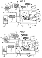
- Figure 2 shows a circuit diagram of a second embodiment in the present invention.
- Figure 3 shows a circuit diagram of a third embodiment in the present invention.
- Figure 4 is a circuit diagram of a fourth embodiment in the present invention.
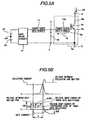
- Figures 5A and 5B are views for explaining the operation of an each embodiment of the present invention.
- Figure 6 is a circuit diagram of an example in the prior art of the present invention.
- Figure 7 shows a relationship between temperature and inner gate resistance in the first embodiment.
- Figure 1A shows a first embodiment. An inner gate resistor (rg) is connected between a
gate electrode 8a of anIGBT chip 1a and agate terminal 4 of anIGBT module 9a, and an outer gate resistor (RG) 11 is connected between theIGBT module 9a and agate circuit 12. Thegate terminal 4 of theIGBT module 9a is connected to an input terminal (B) 15 of avoltage comparing circuit 13, and anauxiliary emitter terminal 5 of theIGBT module 9a is connected to aground terminal 16 of thegate drive circuit 12 and thevoltage comparing circuit 13. Aconstant voltage circuit 18 is connected to an input terminal (A) 14 of thevoltage comparing circuit 13. - Figure 1B is a view showing the inner structure of the
IGBT module 9a. - An
insulator plate 35 is placed on aheat radiating plate 36, andmetal plates insulator plate 35. A collector electrode portion of theIGBT chip 1a is connected to themetal plate 34b, one end of theinner gate resistor 10a is connected to themetal plate 34c, and the other end of theinner gate resistor 10a is connected to a gate electrode portion of theIGBT chip 1a with alead wire 33. Anelectrode 3 for leading out the emitter terminal outside the module, anelectrode 2 for leading out the collector terminal outside the module and anelectrode 4 for leading out the gate terminal outside the module are connected to each of themetal plates - Referring to Figure 1A, when collector current 20 conducting through the
IGBT chip 1a becomes excessively large and temperature of theIGBT chip 1a rises by increase of generated loss of theIGBT chip 1a, temperature of the inner gate resistor (rg) 10a mounting on the same heat radiating plate is also increased. At that time, the value of voltage drop between the both ends of the inner resistor (rg) 10a is changed due to existence of a temperature coefficient of the resistivity which is a physical property possessed by the inner gate resistor (rg) 10a. The change in the voltage drop value of the inner gate resistor (rg) 10a is detected as a voltage (VGE) 21 between the gate and the emitter and input to the input terminal (B) 15 of thevoltage comparing circuit 13. A constant voltage value from theconstant voltage circuit 18 is input to the other input terminal (A) 14 of thevoltage comparing circuit 13, and the result of a voltage comparison performed by thevoltage comparing circuit 13 is output from anoutput terminal 17 of thevoltage comparing circuit 13. - Figure 5A and Figure 5B explain operation of the present embodiment. The timing detecting the change in the voltage drop value generated in the
inner gate resistor 10a of the module is the time, referring to Figure 5B, when the voltage (VGE) 21 between the gate and the emitter of theIGBT module 9a is in a Miller effect occurring period A caused by an action of a feedback capacity existing between the collector electrode and the gate electrode of theIGBT chip 1a at turning-off of theIGBT chip 1a. The gate voltage appearing between the gate and the emitter of theIGBT chip 1a in the Miller effect occurring period A described above is a constant value, and the gate current value is a constant value. - The voltage generated between the
gate terminal 4 and theauxiliary emitter terminal 5 having theIGBT module 9a shown in Figure 5A is the sum of the constant value of the gate voltage value in the Miller effect occurring period A described above and the voltage value between the both ends of theinner gate resistor 10a of the module. - Operation accompanied the change in the temperature of the IGBT chip in this embodiment will be described below.
- The temperature coefficients of the resistivity possessed by the resistors such as the gate resistor mounted inside the module are positive values.
- Referring to Figure 1A, when the temperature of the
IGBT module 9a is increased, the resistance of the inner gate resistor (rg) 10a is increased depending on the temperature and accordingly the voltage produced in the inner gate resistor (rg) 10a is increased. Therefore, the constant voltage value generated between thegate terminal 4 and theauxiliary emitter terminal 5 in the period of Figure 5B is decreased, and theoutput terminal 17 of the present temperature sensing circuit performs reversed operation when the voltage value is decreased with respect to the constant voltage value applied to the input terminal (A) 14 of thevoltage comparing circuit 13. Depending on the reversed signal ofoutput terminal 17, the other control circuit is operated, for example, the IGBT is turned off. - Referring to Figure 5B, the amount of change (ΔVGE) in the gate voltage produced between the
gate terminal 4 and theauxiliary emitter terminal 5 due to the temperature change of the inner gate resistor (rg) 10a in the period A depends on the ratio of the resistance value rg of the inner gate resistor (rg) 10a to the resistance value RG of the outer gate resistor (RG) 11. Letting the temperature coefficient of the inner gate resistor (rg) be α, the voltage output from thegate drive circuit 12 in the period A be VGN, and the gate threshold voltage possessed by theIGBT chip 1a depending on a collector current 20 conducting in theIGBT module 9a be VTH, the amount of change ΔVGE in the gate voltage can be expressed by Equation 1.
- According to this equation 1, the temperature change of the inner gate resistor of the module in the period A shown in Figure 5B can be grasped as the amount of change ΔVGE in the gate voltage produced between the
gate terminal 4 and theauxiliary emitter terminal 5. - Therefore, the temperature of the
IGBT module 9a can be detected by connecting a calculator for calculating temperature based on the equation 1 by inputting the gate voltage instead of the voltage comparing circuit. - Temperature sensing in the present embodiment will be described below in detail.
- Referring to Figure 1A, when collector current 20 conducting through the
IGBT chip 1a becomes excessively large and temperature of theIGBT chip 1a is increased from 25°C to 125°C corresponding to increase of generated loss of theIGBT chip 1a, the resistance of the inner gate resistor (rg) 10a is increased to approximately twice the value, as shown in Figure 7, and the gate voltage produced between thegate terminal 4 and theauxiliary emitter terminal 5 changes. An example in Figure 5B will be calculated using the equation 1 for the amount of change ΔVGE in the gate voltage. Assuming that VGP = 15 V, VGN = 10 V, VTH = 8 V, RG = 10 Ω, rg = 2Ω (at 25°C) and rg =4 Ω (at 125°C), the results become that ΔVGE = 3 V at 25°C and Δ VGE = 5.1 V at 125°C, and the difference 2.1 V is the amount of change in the gate voltage caused by the temperature rise. That is, in Figure 5B, the constant voltage values of the gate voltage in the period A are 5 V at 25°C and 2.9 V at 125°C. These voltage values are compared with the constant voltage value applied to the input terminal (A) 14 of thevoltage comparing circuit 13 of Figure 1A, and the output of the present temperature sensing device performed reversed operation when the voltage is decreased. For example, when the voltage of the input terminal (A) 14 of thevoltage comparing circuit 13 is assumed to be 3 V, the voltage of the input terminal (B) 15 of thevoltage comparing circuit 13 is changed from 5 V to 2.9 V to the temperature rise in theIGBT module 9a from 25°C to 125°C, and therefore, temperature sensing operation is performed because the voltage of the input terminal (B) 15 becomes lower than the applied voltage of the input terminal (A) 14. - Figure 2 shows a second embodiment. This embodiment is a case where a plurality of IGBTs are connected in parallel. An inner gate resistor (rg) 10a and an inner gate resistor (rt) 22 are connected in series between a
gate electrode 8a of anIGBT 1a and agate terminal 4 of anIGBT module 9b, and an outer gate resistor (RG) 11 is connected between thegate terminal 4 of anIGBT module 9b and agate drive circuit 12. Thegate terminal 4 of the IGBT module 9bis connected to an input terminal (B) 15 of avoltage comparing circuit 13, and anauxiliary terminal 5 of theIGBT module 9b is connected to aground terminal 16 of thegate drive circuit 12 and thevoltage comparing circuit 12. Aconstant voltage circuit 18 is connected to an input terminal (A) 14 of thevoltage comparing circuit 13. Further, acollector electrode 6b of theIGBT 1b is connected to acollector electrode 6a of theIGBT 1a, anemitter electrode 7b of theIGBT 1b is connected to anemitter electrode 7a of theIGBT 1a, and an inner gate resistor (rg) 10b is connected between thegate electrode 22 of theIGBT 1b and point B 23 (that is, a junction point of theinner gate resistor 22 and theinner gate resistor 10a) of one end of the inner gate resistor (rt) 22. - Referring to Figure 2, when the inner gate resistor (rg) 10a of the
IGBT 1a and the inner gate resistor (rg) 10b of theIGBT 1b are connected in parallel, an amount of change in the sensing level is decreased because the composite resistance becomes small and accordingly the produced voltage drop is decreased. Therefore, in order to increase the sensing level, the composite resistance is increased to increase the produced voltage drop by connecting the inner gate resistor (rt) 22 to the inner gate resistors (rg) 10a and 10b in series. - As shown in Figure 5B, the timing of temperature sensing is performed in the period A when the voltage (VGE) 21 between the gate and the emitter of the
IGBT module 9b becomes a clamp voltage at turning-off of theIGBT 1a and theIGBT 1b. In general, a voltage drop is produced in the inner gate resistor by gate current 19 flowing at turning-off of theIGBT 1a and theIGBT 1b to decrease the clamp voltage. Referring to Figure 2, when the temperature of theIGBT module 9b is increased, the composite resistance of the inner gate resistor is increased depending on the temperature and accordingly the voltage produced in the composite inner gate resistor is increased. Therefore, the clamp voltage in the period of Figure 5B is further decreased, and the present temperature sensing circuit is operated when the voltage value is decreased with respect to the constant voltage value applied to the input terminal (A) 14 of thevoltage comparing circuit 13. - Referring to Figure 5B, the amount of change (ΔVGE) in the clamp voltage due to the temperature change of the inner gate resistor in the period A is determined by the ratio of the composite resistance of the inner gate resistors (rg) 10a, 10b and the inner gate resistor (rt) 22 to the resistance of the outer gate resistor (RG) 11. Letting the temperature coefficient of the composite inner gate resistor be α, the composite inner gate resistance be r, the negative voltage applied to the
gate terminal 4 be VGN, and the clamp voltage depending on a collector current 20 conducting in theIGBT module 9b be VTH, the amount of change (ΔVGE) in the clamp voltage due to the temperature change of the inner gate resistor in the period A can be expressed byEquation 2.
- The temperature change can be detected based on ΔVGE similarly to the first embodiment.
- Figure 3 shows a third embodiment. This embodiment is a case where a plurality of IGBTs are also connected in parallel. An inner gate resistor (rg) 10a and an inner gate resistor (rt) 22 are connected in series between a
gate electrode 8a of anIGBT 1a and agate terminal 4 of anIGBT module 9b, and an outer gate resistor (RG) 11 is connected between thegate terminal 4 of anIGBT module 9b and agate drive circuit 12. Thegate terminal 4 of the IGBT module 9bis connected to an input terminal (B) 15 of avoltage comparing circuit 13, and anauxiliary terminal 5 of theIGBT module 9b is connected to aground terminal 16 of thegate drive circuit 12 and thevoltage comparing circuit 12. Aconstant voltage circuit 18 is connected to an input terminal (A) 14 of thevoltage comparing circuit 13. Further, acollector electrode 6b of theIGBT 1b is connected to acollector electrode 6a of theIGBT 1a, anemitter electrode 7b of theIGBT 1b is connected to anemitter electrode 7a of theIGBT 1a, and an inner gate resistor (rg) 10b is connected between thegate electrode 22 of theIGBT 1b and point B 23 (that is, a junction point of theinner gate resistor 22 and theinner gate resistor 10a) of one end of the inner gate resistor (rt) 22. Further, atemperature sensing terminal 24 is provided and connected to thepoint 23. - Referring to Figure 3, when the inner gate resistor (rg) 10a of the
IGBT 1a and the inner gate resistor (rg) 10b of theIGBT 1b are connected in parallel, an amount of change in the sensing level is decreased because the composite resistance becomes small and accordingly the produced voltage drop is decreased. Therefore, by connecting the inner gate resistor (rt) 22 to the inner gate resistors (rg) 10a and 10b in series and further providing thetemperature sensing terminal 24 to thepoint B 23 of the one end of the inner gate resistor (rt) 22, temperature detecting operation is performed by detecting the terminal voltage of the inner gate resistor (rt) 22. - Similarly to Figure 5B, the timing of temperature sensing is performed by the voltage (VTG) between the
temperature sensing terminal 24 and thegate terminal 4 in the period A when the voltage (VGE) 21 between the gate and the emitter of theIGBT module 9b becomes a clamp voltage at turning-off of theIGBT 1a and theIGBT 1b. In general, the voltage (VTG) 25 is generated in the inner gate transistor (rt) 22 by the gate current 19 flowing at turning-off of theIGBT 1a and theIGBT 1b to decrease the clamp voltage. Referring to Figure 3, when the temperature of theIGBT module 9b is increased, the resistance of the inner gate resistor (rt) 22 is increased depending on the temperature and the voltage produced in theinner gate resistor 22 is further increased. Then, the present temperature sensing circuit is operated when the voltage value is increased with respect to the constant voltage value applied to the input terminal (A) 14 of thevoltage comparing circuit 13. - Referring to Figure 3, letting the temperature coefficient of the inner gate resistor (rt) 22 be α, and the gate current be Ig, the amount of change (ΔVTG) in the voltage produced in the inner gate resistor (rt) 22 by the temperature rise in the period A can be expressed by
Equation 3.
- Similarly to the case of ΔVGE, the temperature change can be detected from the change ΔVTG in the gate voltage.
- Figure 4 shows a fourth embodiment. In the circuit structure of the third embodiment, the output of the
voltage comparing circuit 13 is connected to thecontrol circuit 26, and the output of thecontrol circuit 26 is connected to thegate drive circuit 12. - In the third embodiment, when the terminal voltage of the
inner gate resistor 22 is decreased to a value lower than the voltage of the input terminal (A) 14 of the voltage comparing circuit, thevoltage comparing circuit 13 regards it as occurrence of abnormality and outputs a signal indicating the abnormality to thecontrol circuit 26. Thecontrol circuit 26 outputs an off operation instruction to the gate drive circuit when receiving the signal indicating the abnormality. When the gate drive circuit receives the off operation instruction, the drive circuit performs turning-off drive of theIGBT 1a and theIGBT 1b. - In the above embodiments, an IGBT is used as the switching element. However, In a case of using a voltage drive type switching element such as a power MOSET, the circuit operation is the same as in the above, and the same effect can be attained.
- According to the present invention, by connecting a resistor for temperature sensing to a voltage drive type semiconductor device, it is possible to provide a high reliable temperature sensing circuit.
Claims (7)
- A temperature sensing circuit for a voltage drive type semiconductor device, which comprises a first semiconductor element (1a) controlling the current flow between a pair of main electrodes (6a, 7a) by a voltage applied to a first insulated gate electrode (8a), a gate terminal (4) connected to said first insulated gate electrode (8a), and another terminal (5) connected to one of said main electrodes (6a, 7a), comprising
a resistor (10a) having a positive temperature coefficient connected between said gate terminal (4) and said insulated gate electrode (8a), and
means for receiving a voltage including a voltage drop across said resistor (10a) in a circuit portion between said gate terminal (4) and said other terminal (5) and sensing the temperature of said voltage drive type semiconductor device based on said voltage,
characterised in that said voltage is a voltage during a Miller effect being generated when said first semiconductor element (1a) turns off. - The circuit of claim 1, wherein said resistor (10a) is contained in said voltage drive type semiconductor device.
- The circuit of claim 1, wherein
said voltage drive type semiconductor device comprises a second semiconductor element (1b) having a second insulated gate electrode (8b) and connected in parallel with said first semiconductor element (1a),and
said resistor comprises a first resistor (10a) and a second resistor (22) connected in series to each other, and a third resistor (10b) connected between the junction point (23) of said first and second resistors (10a, 22) and the second gate electrode (8b). - The circuit of claim 3, wherein said voltage is that between said gate terminal (4) and said other terminal (5), or between said gate terminal (4) and said junction point (23)
- A temperature sensing method for a voltage drive type semiconductor device, which comprises a semiconductor element (1a) controlling the current flow between a pair of main electrodes by a voltage applied to an insulated gate electrode (8a), a gate terminal (4) connected to said insulated gate electrode (8a), and another terminal (5) connected to one of said main electrodes (6a, 7a), the method comprising the steps of:connecting a resistor (10a) having a positive temperature coefficient between said gate terminal (4) and said insulated gate electrode (8a), andsensing the temperature of said voltage drive type semiconductor device based on a voltage including a voltage drop across said resistor (10a) in a circuit portion between said gate terminal (4) and said other terminal (5)characterised in that said voltage is a voltage during a Miller effect being generated when said semiconductor element (1a) turns off.
- A drive device for a voltage drive type semiconductor device, which comprises a first semiconductor element(1a) controlling the current flow between a pair of main electrodes (6a, 7a) by a voltage applied to a first insulated gate electrode (8a), a gate terminal (4) connectedto said first insulated gate electrode (8a), and another terminal (5) connected to one of said main electrodes (6a, 7a), comprising
a drive circuit connected to the gate terminal (4) through a resistor (10a) and connected to said other terminal (5), and
the temperature sensing circuit of any one of claims 1 to 4. - The device of claim-6, further comprising a control circuit receiving a signal output from said temperature sensing circuit when a temperature rise is detected, and giving an OFF operation instruction to said drive circuit.
Applications Claiming Priority (2)
| Application Number | Priority Date | Filing Date | Title |
|---|---|---|---|
| JP28906098A JP3599575B2 (en) | 1998-10-12 | 1998-10-12 | Temperature detecting circuit of voltage-driven semiconductor device, driving device using the same, and voltage-driven semiconductor device |
| JP28906098 | 1998-10-12 |
Publications (3)
| Publication Number | Publication Date |
|---|---|
| EP0994565A2 EP0994565A2 (en) | 2000-04-19 |
| EP0994565A3 EP0994565A3 (en) | 2003-09-17 |
| EP0994565B1 true EP0994565B1 (en) | 2006-05-03 |
Family
ID=17738312
Family Applications (1)
| Application Number | Title | Priority Date | Filing Date |
|---|---|---|---|
| EP99118891A Expired - Lifetime EP0994565B1 (en) | 1998-10-12 | 1999-09-24 | Temperature sensing in voltage drive type semiconductor device |
Country Status (4)
| Country | Link |
|---|---|
| US (1) | US6288597B1 (en) |
| EP (1) | EP0994565B1 (en) |
| JP (1) | JP3599575B2 (en) |
| DE (1) | DE69931120T2 (en) |
Families Citing this family (21)
| Publication number | Priority date | Publication date | Assignee | Title |
|---|---|---|---|---|
| US7443225B2 (en) * | 2006-06-30 | 2008-10-28 | Alpha & Omega Semiconductor, Ltd. | Thermally stable semiconductor power device |
| US7988354B2 (en) * | 2007-12-26 | 2011-08-02 | Infineon Technologies Ag | Temperature detection for a semiconductor component |
| EP2472707B1 (en) * | 2009-08-27 | 2017-01-04 | Fuji Electric Co., Ltd. | Semiconductor drive device |
| DE102010029147B4 (en) * | 2010-05-20 | 2012-04-12 | Semikron Elektronik Gmbh & Co. Kg | Method for determining the temperature of a power semiconductor |
| CN103493372A (en) * | 2011-04-28 | 2014-01-01 | 皇家飞利浦有限公司 | Digitally controlled high speed high voltage gate driver circuit |
| JP6044215B2 (en) * | 2012-09-13 | 2016-12-14 | 富士電機株式会社 | Semiconductor device |
| JP6329944B2 (en) * | 2013-05-10 | 2018-05-23 | 株式会社日立製作所 | Control device for insulated gate semiconductor element and power conversion device using the same |
| CN103997839B (en) * | 2014-06-06 | 2018-03-30 | 同方威视技术股份有限公司 | It is a kind of to collimate modulated X-ray emitter |
| US10553381B2 (en) * | 2015-01-20 | 2020-02-04 | Electronics And Telecommunications Research Institute | Electrical switchgear for overcurrent protection using critical temperature device |
| US10069439B2 (en) | 2015-12-22 | 2018-09-04 | Renesas Electronics Corporation | Power conversion system, power module, and semiconductor device with diode coupling |
| JP6750360B2 (en) * | 2016-07-15 | 2020-09-02 | 富士電機株式会社 | Semiconductor device |
| EP3382357B1 (en) * | 2017-03-31 | 2021-03-24 | Mitsubishi Electric R & D Centre Europe B.V. | Device and a method for controlling the temperature of a multi-die power module |
| JP6826499B2 (en) | 2017-06-30 | 2021-02-03 | ルネサスエレクトロニクス株式会社 | Semiconductor devices and power modules |
| US11289993B2 (en) * | 2017-09-25 | 2022-03-29 | Shindengen Electric Manufacturing Co., Ltd. | Switching element control circuit and power module |
| JP6958499B2 (en) * | 2018-07-09 | 2021-11-02 | 三菱電機株式会社 | Semiconductor devices and power converters |
| KR102086519B1 (en) * | 2018-07-12 | 2020-03-09 | 엘지전자 주식회사 | Power transforming apparatus, compressor including the same and method for controlling the same |
| US10948359B2 (en) | 2018-10-30 | 2021-03-16 | Analog Devices International Unlimited Company | Techniques for junction temperature determination of power switches |
| JP7338279B2 (en) * | 2019-07-11 | 2023-09-05 | 富士電機株式会社 | Power semiconductor module and its leakage current test method |
| JP7222880B2 (en) * | 2019-12-26 | 2023-02-15 | キヤノン電子管デバイス株式会社 | X-ray tube packaging device |
| EP3955463A1 (en) * | 2020-08-10 | 2022-02-16 | Siemens Aktiengesellschaft | Parallel circuit of semiconductor switches |
| CN115206180B (en) * | 2022-07-25 | 2023-08-01 | 武汉华星光电技术有限公司 | Display panel and display device |
Family Cites Families (14)
| Publication number | Priority date | Publication date | Assignee | Title |
|---|---|---|---|---|
| DE2252185C2 (en) * | 1972-10-25 | 1983-12-01 | Robert Bosch Gmbh, 7000 Stuttgart | Circuit arrangement for converting and evaluating the output signal of an oxygen sensor in a device for exhaust gas decontamination of internal combustion engines |
| US4220877A (en) * | 1977-05-16 | 1980-09-02 | Rca Corporation | Temperature compensated switching circuit |
| US4914542A (en) * | 1988-12-27 | 1990-04-03 | Westinghouse Electric Corp. | Current limited remote power controller |
| US5045964A (en) * | 1990-04-30 | 1991-09-03 | Motorola, Inc. | Thermal clamp for an ignition coil driver |
| US5444219A (en) * | 1990-09-24 | 1995-08-22 | U.S. Philips Corporation | Temperature sensing device and a temperature sensing circuit using such a device |
| JPH06244413A (en) | 1993-02-22 | 1994-09-02 | Hitachi Ltd | Insulated gate semiconductor device |
| JP3327419B2 (en) | 1993-08-24 | 2002-09-24 | 自動車電機工業株式会社 | Motor control device |
| JP3243902B2 (en) * | 1993-09-17 | 2002-01-07 | 株式会社日立製作所 | Semiconductor device |
| JPH0832361A (en) * | 1994-07-14 | 1996-02-02 | Toyota Autom Loom Works Ltd | Amplifier circuit provided with protection device |
| JP3265849B2 (en) * | 1994-09-16 | 2002-03-18 | 富士電機株式会社 | Self-extinguishing element with overheat protection device |
| JP3302193B2 (en) * | 1994-10-06 | 2002-07-15 | 株式会社東芝 | Current detection circuit |
| JPH09119870A (en) | 1995-10-26 | 1997-05-06 | Nec Corp | Temperature detecting method, semiconductor device, and temperature detecting circuit |
| US5723916A (en) * | 1996-05-17 | 1998-03-03 | Delco Electronics Corporation | Electrical load driving device including load current limiting circuitry |
| WO1998037581A2 (en) * | 1997-02-19 | 1998-08-27 | Koninklijke Philips Electronics N.V. | Power semiconductor devices with a temperature sensor circuit |
-
1998
- 1998-10-12 JP JP28906098A patent/JP3599575B2/en not_active Expired - Fee Related
-
1999
- 1999-09-24 EP EP99118891A patent/EP0994565B1/en not_active Expired - Lifetime
- 1999-09-24 DE DE69931120T patent/DE69931120T2/en not_active Expired - Fee Related
- 1999-10-12 US US09/416,650 patent/US6288597B1/en not_active Expired - Lifetime
Also Published As
| Publication number | Publication date |
|---|---|
| US6288597B1 (en) | 2001-09-11 |
| EP0994565A2 (en) | 2000-04-19 |
| EP0994565A3 (en) | 2003-09-17 |
| DE69931120T2 (en) | 2006-12-21 |
| DE69931120D1 (en) | 2006-06-08 |
| JP3599575B2 (en) | 2004-12-08 |
| JP2000124781A (en) | 2000-04-28 |
Similar Documents
| Publication | Publication Date | Title |
|---|---|---|
| EP0994565A2 (en) | Temperature sensing in voltage drive type semiconductor device | |
| US5187632A (en) | Controllable semiconductor switching device having integrated current limitation and overheating disconnection | |
| EP1028467B1 (en) | Semiconductor active fuse for AC power line and bidirectional switching device for the fuse | |
| JP4929020B2 (en) | Overcurrent protection device for load circuit | |
| EP1028526B1 (en) | Switching device with weak-current detecting function | |
| EP1017173A2 (en) | Power supply control device and method of controlling the same | |
| CN113949327B (en) | Power modules for operating electric vehicle drives | |
| CN110865290A (en) | Power semiconductor circuit and method for determining the temperature of a power semiconductor device | |
| CN102195282A (en) | Current limiting circuit | |
| US5581432A (en) | Clamp circuit and method for identifying a safe operating area | |
| US11929354B2 (en) | Power semiconductor module | |
| EP0702455A2 (en) | Overheat protection apparatus for self-turn-off device | |
| JP2003274672A (en) | Semiconductor switching device | |
| CN110611298B (en) | IPM protection system for flywheel energy storage device | |
| JP7306710B2 (en) | Electrical device testing equipment | |
| CN219739944U (en) | Overcurrent protection circuit, control switch and vehicle | |
| US20250247089A1 (en) | Power Device, Electronic Device, and Circuit Structure | |
| JP3311498B2 (en) | Semiconductor device | |
| JPH07221261A (en) | Power semiconductor device with temperature sensor | |
| US12283898B2 (en) | Method for detecting a characteristic operating parameter of a transistor of an inverter | |
| JPH0832361A (en) | Amplifier circuit provided with protection device | |
| JP2002110986A (en) | Semiconductor device | |
| JPH0854427A (en) | Semiconductor element current detection device | |
| JP2020197384A (en) | Current measuring device, current measuring method and program | |
| JP2003152513A (en) | Temperature-balancing circuit for semiconductor device |
Legal Events
| Date | Code | Title | Description |
|---|---|---|---|
| PUAI | Public reference made under article 153(3) epc to a published international application that has entered the european phase |
Free format text: ORIGINAL CODE: 0009012 |
|
| AK | Designated contracting states |
Kind code of ref document: A2 Designated state(s): AT BE CH CY DE DK ES FI FR GB GR IE IT LI LU MC NL PT SE |
|
| AX | Request for extension of the european patent |
Free format text: AL;LT;LV;MK;RO;SI |
|
| PUAL | Search report despatched |
Free format text: ORIGINAL CODE: 0009013 |
|
| AK | Designated contracting states |
Kind code of ref document: A3 Designated state(s): AT BE CH CY DE DK ES FI FR GB GR IE IT LI LU MC NL PT SE |
|
| AX | Request for extension of the european patent |
Extension state: AL LT LV MK RO SI |
|
| 17P | Request for examination filed |
Effective date: 20040311 |
|
| 17Q | First examination report despatched |
Effective date: 20040427 |
|
| AKX | Designation fees paid |
Designated state(s): CH DE LI |
|
| GRAP | Despatch of communication of intention to grant a patent |
Free format text: ORIGINAL CODE: EPIDOSNIGR1 |
|
| GRAS | Grant fee paid |
Free format text: ORIGINAL CODE: EPIDOSNIGR3 |
|
| GRAA | (expected) grant |
Free format text: ORIGINAL CODE: 0009210 |
|
| AK | Designated contracting states |
Kind code of ref document: B1 Designated state(s): CH DE LI |
|
| REG | Reference to a national code |
Ref country code: CH Ref legal event code: NV Representative=s name: TROESCH SCHEIDEGGER WERNER AG Ref country code: CH Ref legal event code: EP |
|
| REF | Corresponds to: |
Ref document number: 69931120 Country of ref document: DE Date of ref document: 20060608 Kind code of ref document: P |
|
| PLBE | No opposition filed within time limit |
Free format text: ORIGINAL CODE: 0009261 |
|
| STAA | Information on the status of an ep patent application or granted ep patent |
Free format text: STATUS: NO OPPOSITION FILED WITHIN TIME LIMIT |
|
| 26N | No opposition filed |
Effective date: 20070206 |
|
| PGFP | Annual fee paid to national office [announced via postgrant information from national office to epo] |
Ref country code: CH Payment date: 20080723 Year of fee payment: 10 |
|
| PGFP | Annual fee paid to national office [announced via postgrant information from national office to epo] |
Ref country code: DE Payment date: 20080908 Year of fee payment: 10 |
|
| REG | Reference to a national code |
Ref country code: CH Ref legal event code: PL |
|
| PG25 | Lapsed in a contracting state [announced via postgrant information from national office to epo] |
Ref country code: DE Free format text: LAPSE BECAUSE OF NON-PAYMENT OF DUE FEES Effective date: 20100401 |
|
| PG25 | Lapsed in a contracting state [announced via postgrant information from national office to epo] |
Ref country code: LI Free format text: LAPSE BECAUSE OF NON-PAYMENT OF DUE FEES Effective date: 20090930 Ref country code: CH Free format text: LAPSE BECAUSE OF NON-PAYMENT OF DUE FEES Effective date: 20090930 |