EP0994446A2 - System zur Verarbeitung von Informationen und Informationsträger - Google Patents
System zur Verarbeitung von Informationen und Informationsträger Download PDFInfo
- Publication number
- EP0994446A2 EP0994446A2 EP99119433A EP99119433A EP0994446A2 EP 0994446 A2 EP0994446 A2 EP 0994446A2 EP 99119433 A EP99119433 A EP 99119433A EP 99119433 A EP99119433 A EP 99119433A EP 0994446 A2 EP0994446 A2 EP 0994446A2
- Authority
- EP
- European Patent Office
- Prior art keywords
- access
- memory
- information
- data processing
- processing unit
- Prior art date
- Legal status (The legal status is an assumption and is not a legal conclusion. Google has not performed a legal analysis and makes no representation as to the accuracy of the status listed.)
- Granted
Links
Images
Classifications
-
- G—PHYSICS
- G07—CHECKING-DEVICES
- G07F—COIN-FREED OR LIKE APPARATUS
- G07F7/00—Mechanisms actuated by objects other than coins to free or to actuate vending, hiring, coin or paper currency dispensing or refunding apparatus
- G07F7/08—Mechanisms actuated by objects other than coins to free or to actuate vending, hiring, coin or paper currency dispensing or refunding apparatus by coded identity card or credit card or other personal identification means
- G07F7/10—Mechanisms actuated by objects other than coins to free or to actuate vending, hiring, coin or paper currency dispensing or refunding apparatus by coded identity card or credit card or other personal identification means together with a coded signal, e.g. in the form of personal identification information, like personal identification number [PIN] or biometric data
-
- G—PHYSICS
- G06—COMPUTING OR CALCULATING; COUNTING
- G06Q—INFORMATION AND COMMUNICATION TECHNOLOGY [ICT] SPECIALLY ADAPTED FOR ADMINISTRATIVE, COMMERCIAL, FINANCIAL, MANAGERIAL OR SUPERVISORY PURPOSES; SYSTEMS OR METHODS SPECIALLY ADAPTED FOR ADMINISTRATIVE, COMMERCIAL, FINANCIAL, MANAGERIAL OR SUPERVISORY PURPOSES, NOT OTHERWISE PROVIDED FOR
- G06Q20/00—Payment architectures, schemes or protocols
- G06Q20/30—Payment architectures, schemes or protocols characterised by the use of specific devices or networks
- G06Q20/34—Payment architectures, schemes or protocols characterised by the use of specific devices or networks using cards, e.g. integrated circuit [IC] cards or magnetic cards
- G06Q20/341—Active cards, i.e. cards including their own processing means, e.g. including an IC or chip
-
- G—PHYSICS
- G06—COMPUTING OR CALCULATING; COUNTING
- G06Q—INFORMATION AND COMMUNICATION TECHNOLOGY [ICT] SPECIALLY ADAPTED FOR ADMINISTRATIVE, COMMERCIAL, FINANCIAL, MANAGERIAL OR SUPERVISORY PURPOSES; SYSTEMS OR METHODS SPECIALLY ADAPTED FOR ADMINISTRATIVE, COMMERCIAL, FINANCIAL, MANAGERIAL OR SUPERVISORY PURPOSES, NOT OTHERWISE PROVIDED FOR
- G06Q20/00—Payment architectures, schemes or protocols
- G06Q20/30—Payment architectures, schemes or protocols characterised by the use of specific devices or networks
- G06Q20/34—Payment architectures, schemes or protocols characterised by the use of specific devices or networks using cards, e.g. integrated circuit [IC] cards or magnetic cards
- G06Q20/346—Cards serving only as information carrier of service
-
- G—PHYSICS
- G06—COMPUTING OR CALCULATING; COUNTING
- G06Q—INFORMATION AND COMMUNICATION TECHNOLOGY [ICT] SPECIALLY ADAPTED FOR ADMINISTRATIVE, COMMERCIAL, FINANCIAL, MANAGERIAL OR SUPERVISORY PURPOSES; SYSTEMS OR METHODS SPECIALLY ADAPTED FOR ADMINISTRATIVE, COMMERCIAL, FINANCIAL, MANAGERIAL OR SUPERVISORY PURPOSES, NOT OTHERWISE PROVIDED FOR
- G06Q20/00—Payment architectures, schemes or protocols
- G06Q20/30—Payment architectures, schemes or protocols characterised by the use of specific devices or networks
- G06Q20/34—Payment architectures, schemes or protocols characterised by the use of specific devices or networks using cards, e.g. integrated circuit [IC] cards or magnetic cards
- G06Q20/357—Cards having a plurality of specified features
- G06Q20/3576—Multiple memory zones on card
- G06Q20/35765—Access rights to memory zones
-
- G—PHYSICS
- G07—CHECKING-DEVICES
- G07F—COIN-FREED OR LIKE APPARATUS
- G07F7/00—Mechanisms actuated by objects other than coins to free or to actuate vending, hiring, coin or paper currency dispensing or refunding apparatus
- G07F7/08—Mechanisms actuated by objects other than coins to free or to actuate vending, hiring, coin or paper currency dispensing or refunding apparatus by coded identity card or credit card or other personal identification means
- G07F7/10—Mechanisms actuated by objects other than coins to free or to actuate vending, hiring, coin or paper currency dispensing or refunding apparatus by coded identity card or credit card or other personal identification means together with a coded signal, e.g. in the form of personal identification information, like personal identification number [PIN] or biometric data
- G07F7/1008—Active credit-cards provided with means to personalise their use, e.g. with PIN-introduction/comparison system
Definitions
- the invention relates to a system for processing information and an information carrier.
- a portable information carrier especially in a smart card
- stored information is common stored in different files.
- These files each have a first area in which the information are stored, and have another area on, in the control information or access information of the file in question. Access to a record A file is only possible if the corresponding access conditions are fulfilled.
- a disadvantage of the known File structure is that each file has a limited scope can store information. If more than one user Access to the assigned information is granted , it is necessary to give each user their own Assign file with corresponding access conditions. The disadvantage of this, however, is that if access is enabled of the same information to different users a considerable memory requirement is required.
- the object of the invention is therefore a system for processing of information and to provide an information carrier so that an access of a plurality of different Allows users to access information stored in the chip card is, the memory requirement on the chip card is as low as possible.
- the particular advantage of the invention is that a Access zone created with a multi-dimensional access field that will have access to everyone in the files of the Controls stored smart card information.
- the access field is formed like a matrix and on the one hand Encryption vectors, each with access information to different areas of those stored in the chip card Show information.
- the access field can easily be expanded, for example if a user is added. In this case only needs another encryption vector can be generated, which the contains access information assigned to the user.
- the storage index vector can remain unchanged if none further information should be saved. Consequently can easily be accessed by a plurality of stored information to a plurality of users to be controlled.
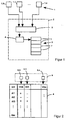
- Figure 1 is a system for processing information shown, which consists of a plurality of data processing units 1, 1.0, 1.1, 1.n, each with a chip card 2 can communicate.
- the data processing units 1 are each via a card reader, not shown connectable to the chip card 2, so that information bidirectionally between a data processing unit 1 and the chip card 2 can be replaced.
- the chip card 2 has a microprocessor, not shown on the communication between the smart card 2 and controls one of the data processing units 1.
- the information are stored in a memory 3 on the chip card 2.
- the memory 3 is preferably an EEPROM memory formed and has a plurality of data records 7, in each of which information is stored.
- the memory 3 is an access field 4 assigned that the access rights of individual data processing units 1 to those in the memory 3 stored information set.
- the chip card 2 has an authentication unit 5 which ensures that an external data processing unit 1 only gets access to stored information, if the match between a particular one electronic key of a corresponding data processing unit 1, 1.0, 1.1, 1.n with one for this data processing unit 1, 1.0, 1.1, 1.n assigned key 6, 6.0, 6.1, 6.n is determined on chip card 2.
- the access zone 4 is matrix-like built up. It has a plurality of columns with a first column by a memory index vector SIV and other columns as encryption vectors VV0, VV1 etc. are trained.
- the memory index vector SIV has the assignment functions or memory addresses AI1, AI2, ... AIm of each stored in the memory 3 as data records Information on.
- the encryption vectors VV0, VV1, ... VVn each have access information and are the assigned to individual data processing units 1.0, 1.1, ... 1.n.
- the data processing unit 1.1 As soon as, for example, a key 6.1 of the data processing unit 1.1 by a comparison in the authentication unit 5 checked and if the result is positive, the data processing unit 1.1 has been identified the access information stored in the encryption vector VV1 the data processing unit 1.1 the specified accessible memory addresses. In the present The data processing unit 1.1 only the memory address AI3 assigned (by a Circle marked). The other addresses AI1, AI2 etc. are before access by the data processing unit 1.1 protected.
- the encryption vector VV0 of the first data processing unit 1.0, the memory addresses AI1 and AI3 are assigned.
- the memory address AI2 is the encryption vector VV0 not assigned, so that only those identified by addresses AI1 and AI3 marked records 7 are accessible.
- this access field 4 is arbitrary depending on the number of additional data processing units can be expanded. All that is needed is another encryption vector generated and stored in the EEPROM memory become.
- the invention can be used wherever multiple users Access to a part of the the memory 3 of the chip card 2 stored information should be granted.
- the invention could for example Serve to simplify the waiver procedure.
- the Asylum seekers a chip card that contains all relevant information such as. Name, date of birth, nationality etc. contains.
- Theembassy seeker can use an encryption vector be assigned access to all stored information enables.
- Any authority such as the Immigration or registration authorities can use an encryption vector assigned, which defines the access rights. Each authority can do this through the encryption vector Assigned information that is assigned before are protected from access by other authorities. So it will on the one hand increases data security and on the other hand one Abuse of government benefits prevented. Because the Chip card with the writable memory 3 serves as an information carrier, in which all the necessary information is always available can be updated.
Landscapes
- Engineering & Computer Science (AREA)
- Business, Economics & Management (AREA)
- Physics & Mathematics (AREA)
- General Physics & Mathematics (AREA)
- Computer Networks & Wireless Communication (AREA)
- Accounting & Taxation (AREA)
- Strategic Management (AREA)
- Microelectronics & Electronic Packaging (AREA)
- General Business, Economics & Management (AREA)
- Theoretical Computer Science (AREA)
- Storage Device Security (AREA)
- Credit Cards Or The Like (AREA)
- Information Retrieval, Db Structures And Fs Structures Therefor (AREA)
- Thermal Transfer Or Thermal Recording In General (AREA)
Abstract
Description
- Figur 1:
- ein Blockschaltbild eines erfindungsgemäßen Systems und
- Figur 2:
- eine schematische Darstellung eines Zugriffsfelds.
Claims (7)
- System zur Verarbeitung von Informationen mitdie Zugriffszone als mehrdimensionales Zugriffsfeld (4) ausgebildet ist mit einer zu der Anzahl der Datenverarbeitungseinheiten (1, 1.0, 1.1, 1.n) korrespondierenden Anzahl von Verschlüsselungsvektoren (VV0, VV1), die jeweils Zugriffsinformationen über den Zugriff auf unterschiedliche Bereiche (7) des Speichers (4) aufweisen, und mit einem die Bereiche (7) kennzeichnenden Adressen (AI1, AI2) aufweisenden Speicherindexvektor (SIV).einer Mehrzahl von örtlich verteilt angeordneten Datenverarbeitungseinheiten (1) zur Speicherung und Verarbeitung von Informationen,mindestens einem tragbaren Informationsträger (2) mit einem nicht flüchtigen Speicher (3), der eine Zugriffszone mit Speicherzugriffsbefehlen für den Zugriff auf eine Speicheradresse (AI1, AI2) des Speichers (3) aufweist,einer Schreib/Leseeinheit zur Ermöglichung der Kommunikation zwischen dem Informationsträger (2) und der Datenverarbeitungseinheit (1), wobei
- System nach Anspruch 1, dadurch gekennzeichnet, daß der Verschlüsselungsvektor (VV0, VV1) jeweils einer einzigen Datenverarbeitungseinheit (1.0, 1.1) über einen geheimen Schlüssel (6.0, 6.1) zugreifbar ist.
- System nach Anspruch 1 oder 2, dadurch gekennzeichnet, daß die Datenverarbeitungseinheit (1, 1.0, 1.1, 1.n) jeweils durch Ablauf einer Authentifikation den Zugriff auf den entsprechenden Verschlüsselungsvektor (VV0, VV1) erhält.
- System nach einem der Ansprüche 1 bis 3, dadurch gekennzeichnet, daß die Bereiche des Speichers (3) als fortlaufende Datensätze ausgebildet sind, die einzeln durch Speicheradressen (AI1, AI2) adressierbar sind.
- Informationsträger zur Speicherung und Verarbeitung von Informationen mit einem nicht flüchtigen Speicher und einem Mikroprozessor, wobei der nicht flüchtige Speicher eine Zugriffszone mit Speicherzugriffsbefehlen für den Zugriff auf eine Speicheradresse des Speichers aufweist, dadurch gekennzeichnet, daß die Zugriffszone als mehrdimensionales Zugriffsfeld (4) ausgebildet ist mit einer zu der Anzahl der Datenverarbeitungseinheiten (1, 1.0, 1.1, 1.n) korrespondierenden Anzahl von Verschlüsselungsvektoren (VV0, VV1), die jeweils Zugriffsinformationen über den Zugriff auf unterschiedliche Bereiche (7)des Speichers (4) aufweisen, und mit einem die Bereiche (7) kennzeichnenden Adressen (AI1, AI2) aufweisenden Speicherindexvektor (SIV).
- Informationsträger nach Anspruch 5, dadurch gekennzeichnet, daß die jeweils einer Datenverarbeitungseinheit (1) zugeordneten Verschlüsselungsvektoren (VV0, VV1) eine Reihe von Zugriffsinformationen enthalten, wobei der Zugriff auf die Zugriffsinformationen durch einen Schlüssel gesichert ist.
- Informationsträger nach Anspruch 5 oder 6, dadurch gekennzeichnet, daß die in dem Speicherindexvektor (SIV) gespeicherten Adressen (AI1, AI2) jeweils einen Datensatz des Speichers (3) bezeichnen.
Applications Claiming Priority (2)
| Application Number | Priority Date | Filing Date | Title |
|---|---|---|---|
| DE19847414A DE19847414A1 (de) | 1998-10-14 | 1998-10-14 | System zur Verarbeitung von Informationen und Informationsträger |
| DE19847414 | 1998-10-14 |
Publications (3)
| Publication Number | Publication Date |
|---|---|
| EP0994446A2 true EP0994446A2 (de) | 2000-04-19 |
| EP0994446A3 EP0994446A3 (de) | 2002-06-05 |
| EP0994446B1 EP0994446B1 (de) | 2003-12-17 |
Family
ID=7884482
Family Applications (1)
| Application Number | Title | Priority Date | Filing Date |
|---|---|---|---|
| EP99119433A Expired - Lifetime EP0994446B1 (de) | 1998-10-14 | 1999-09-30 | System zur Verarbeitung von Informationen und Informationsträger |
Country Status (4)
| Country | Link |
|---|---|
| EP (1) | EP0994446B1 (de) |
| AT (1) | ATE256903T1 (de) |
| DE (2) | DE19847414A1 (de) |
| ES (1) | ES2214786T3 (de) |
Family Cites Families (3)
| Publication number | Priority date | Publication date | Assignee | Title |
|---|---|---|---|---|
| US4816653A (en) * | 1986-05-16 | 1989-03-28 | American Telephone And Telegraph Company | Security file system for a portable data carrier |
| EP0332117B1 (de) * | 1988-03-09 | 1994-05-11 | Kabushiki Kaisha Toshiba | Tragbarer elektronischer Apparat |
| US5544246A (en) * | 1993-09-17 | 1996-08-06 | At&T Corp. | Smartcard adapted for a plurality of service providers and for remote installation of same |
-
1998
- 1998-10-14 DE DE19847414A patent/DE19847414A1/de not_active Ceased
-
1999
- 1999-09-30 DE DE59908087T patent/DE59908087D1/de not_active Expired - Lifetime
- 1999-09-30 ES ES99119433T patent/ES2214786T3/es not_active Expired - Lifetime
- 1999-09-30 EP EP99119433A patent/EP0994446B1/de not_active Expired - Lifetime
- 1999-09-30 AT AT99119433T patent/ATE256903T1/de not_active IP Right Cessation
Non-Patent Citations (1)
| Title |
|---|
| None |
Also Published As
| Publication number | Publication date |
|---|---|
| EP0994446A3 (de) | 2002-06-05 |
| DE59908087D1 (de) | 2004-01-29 |
| ATE256903T1 (de) | 2004-01-15 |
| ES2214786T3 (es) | 2004-09-16 |
| EP0994446B1 (de) | 2003-12-17 |
| DE19847414A1 (de) | 2000-04-20 |
Similar Documents
| Publication | Publication Date | Title |
|---|---|---|
| DE69320900T3 (de) | IC-Karte mit hierarchischer Dateienstruktur | |
| DE3811378C3 (de) | Informationsaufzeichnungssystem | |
| EP1065598A1 (de) | Verfahren zum Zugriff auf einen Speicher und Speichereinrichtung hierfür | |
| DE3407642C2 (de) | ||
| DE68915186T2 (de) | Tragbarer elektronischer Apparat. | |
| DE3650156T2 (de) | Auf regeln basiertes datenwiederauffindverfahren und anordnung. | |
| DE19536169A1 (de) | Multifunktionale Chipkarte | |
| DE3523237A1 (de) | Anordnung zum sichern des transports von chipkarten | |
| DE102006032129A1 (de) | Skalierbares Verfahren zur Zugriffssteuerung | |
| EP1358558B1 (de) | Mikroprozessorschaltung für datenträger und verfahren zum organisieren des zugriffs auf in einem speicher abgelegten daten | |
| DE1269393B (de) | Mikroprogramm-Steuerwerk | |
| DE1499182A1 (de) | Elektrische Datenverarbeitungsanlage | |
| EP2905752A2 (de) | ELEKTRONISCHE SCHLIEßANLAGE MIT MEHREREN SCHLIEßZYLINDERN | |
| DE69316779T2 (de) | Tragbares elektronisches Gerät | |
| EP0555303A1 (de) | Zugangskontrollvorrichtung. | |
| DE10124139A1 (de) | Verfahren und Vorrichtung zur Sicherung der Datenübertragung zwischen einem Zentralprozessor und einem Speicher | |
| EP0994446B1 (de) | System zur Verarbeitung von Informationen und Informationsträger | |
| WO2005024703A1 (de) | Datenübertragungssystem und verfahren zum betreiben eines datenübertragungssystems | |
| DE3333894C2 (de) | ||
| EP0459477A2 (de) | Datenträger | |
| DE112006004173T5 (de) | Schutz eines programmierbaren Speichers gegen unberechtigte Veränderung | |
| DE2635180A1 (de) | Verfahren zur elektronisch gesteuerten verriegelung und entriegelung von tuer-, safe- und funktionsschloessern | |
| EP0890172B1 (de) | Halbleiterspeichervorrichtung | |
| DE19508288A1 (de) | Verfahren und Anordnung zur Verhinderung der unberechtigten Nutzung eines Rechners | |
| DE2717065C3 (de) | Einrichtung zur Prüfung der Zuordnung einer Geheimzahl zu einer auf einer Karte gespeicherten Kartenzahl |
Legal Events
| Date | Code | Title | Description |
|---|---|---|---|
| PUAI | Public reference made under article 153(3) epc to a published international application that has entered the european phase |
Free format text: ORIGINAL CODE: 0009012 |
|
| AK | Designated contracting states |
Kind code of ref document: A2 Designated state(s): AT BE CH CY DE DK ES FI FR GB GR IE IT LI LU MC NL PT SE |
|
| AX | Request for extension of the european patent |
Free format text: AL;LT;LV;MK;RO;SI |
|
| PUAL | Search report despatched |
Free format text: ORIGINAL CODE: 0009013 |
|
| AK | Designated contracting states |
Kind code of ref document: A3 Designated state(s): AT BE CH CY DE DK ES FI FR GB GR IE IT LI LU MC NL PT SE |
|
| AX | Request for extension of the european patent |
Free format text: AL;LT;LV;MK;RO;SI |
|
| 17P | Request for examination filed |
Effective date: 20020531 |
|
| 17Q | First examination report despatched |
Effective date: 20020802 |
|
| AKX | Designation fees paid |
Designated state(s): AT BE CH CY DE DK ES FI FR GB GR IE IT LI LU MC NL PT SE |
|
| GRAH | Despatch of communication of intention to grant a patent |
Free format text: ORIGINAL CODE: EPIDOS IGRA |
|
| GRAS | Grant fee paid |
Free format text: ORIGINAL CODE: EPIDOSNIGR3 |
|
| GRAA | (expected) grant |
Free format text: ORIGINAL CODE: 0009210 |
|
| AK | Designated contracting states |
Kind code of ref document: B1 Designated state(s): AT BE CH CY DE DK ES FI FR GB GR IE IT LI LU MC NL PT SE |
|
| PG25 | Lapsed in a contracting state [announced via postgrant information from national office to epo] |
Ref country code: NL Free format text: LAPSE BECAUSE OF FAILURE TO SUBMIT A TRANSLATION OF THE DESCRIPTION OR TO PAY THE FEE WITHIN THE PRESCRIBED TIME-LIMIT Effective date: 20031217 Ref country code: IE Free format text: LAPSE BECAUSE OF FAILURE TO SUBMIT A TRANSLATION OF THE DESCRIPTION OR TO PAY THE FEE WITHIN THE PRESCRIBED TIME-LIMIT Effective date: 20031217 Ref country code: FI Free format text: LAPSE BECAUSE OF FAILURE TO SUBMIT A TRANSLATION OF THE DESCRIPTION OR TO PAY THE FEE WITHIN THE PRESCRIBED TIME-LIMIT Effective date: 20031217 Ref country code: CY Free format text: LAPSE BECAUSE OF FAILURE TO SUBMIT A TRANSLATION OF THE DESCRIPTION OR TO PAY THE FEE WITHIN THE PRESCRIBED TIME-LIMIT Effective date: 20031217 |
|
| REG | Reference to a national code |
Ref country code: GB Ref legal event code: FG4D Free format text: NOT ENGLISH |
|
| REG | Reference to a national code |
Ref country code: CH Ref legal event code: EP |
|
| REG | Reference to a national code |
Ref country code: IE Ref legal event code: FG4D Free format text: GERMAN |
|
| REF | Corresponds to: |
Ref document number: 59908087 Country of ref document: DE Date of ref document: 20040129 Kind code of ref document: P |
|
| PG25 | Lapsed in a contracting state [announced via postgrant information from national office to epo] |
Ref country code: SE Free format text: LAPSE BECAUSE OF FAILURE TO SUBMIT A TRANSLATION OF THE DESCRIPTION OR TO PAY THE FEE WITHIN THE PRESCRIBED TIME-LIMIT Effective date: 20040317 Ref country code: GR Free format text: LAPSE BECAUSE OF FAILURE TO SUBMIT A TRANSLATION OF THE DESCRIPTION OR TO PAY THE FEE WITHIN THE PRESCRIBED TIME-LIMIT Effective date: 20040317 Ref country code: DK Free format text: LAPSE BECAUSE OF FAILURE TO SUBMIT A TRANSLATION OF THE DESCRIPTION OR TO PAY THE FEE WITHIN THE PRESCRIBED TIME-LIMIT Effective date: 20040317 |
|
| GBT | Gb: translation of ep patent filed (gb section 77(6)(a)/1977) |
Effective date: 20040505 |
|
| NLV1 | Nl: lapsed or annulled due to failure to fulfill the requirements of art. 29p and 29m of the patents act | ||
| REG | Reference to a national code |
Ref country code: IE Ref legal event code: FD4D |
|
| REG | Reference to a national code |
Ref country code: ES Ref legal event code: FG2A Ref document number: 2214786 Country of ref document: ES Kind code of ref document: T3 |
|
| PG25 | Lapsed in a contracting state [announced via postgrant information from national office to epo] |
Ref country code: MC Free format text: LAPSE BECAUSE OF NON-PAYMENT OF DUE FEES Effective date: 20040930 Ref country code: LU Free format text: LAPSE BECAUSE OF NON-PAYMENT OF DUE FEES Effective date: 20040930 Ref country code: LI Free format text: LAPSE BECAUSE OF NON-PAYMENT OF DUE FEES Effective date: 20040930 Ref country code: CH Free format text: LAPSE BECAUSE OF NON-PAYMENT OF DUE FEES Effective date: 20040930 Ref country code: BE Free format text: LAPSE BECAUSE OF NON-PAYMENT OF DUE FEES Effective date: 20040930 Ref country code: AT Free format text: LAPSE BECAUSE OF NON-PAYMENT OF DUE FEES Effective date: 20040930 |
|
| ET | Fr: translation filed | ||
| PLBE | No opposition filed within time limit |
Free format text: ORIGINAL CODE: 0009261 |
|
| STAA | Information on the status of an ep patent application or granted ep patent |
Free format text: STATUS: NO OPPOSITION FILED WITHIN TIME LIMIT |
|
| 26N | No opposition filed |
Effective date: 20040920 |
|
| BERE | Be: lapsed |
Owner name: *ORGA KARTENSYSTEME G.M.B.H. Effective date: 20040930 |
|
| REG | Reference to a national code |
Ref country code: CH Ref legal event code: PL |
|
| BERE | Be: lapsed |
Owner name: *ORGA KARTENSYSTEME G.M.B.H. Effective date: 20040930 |
|
| PG25 | Lapsed in a contracting state [announced via postgrant information from national office to epo] |
Ref country code: PT Free format text: LAPSE BECAUSE OF NON-PAYMENT OF DUE FEES Effective date: 20040517 |
|
| REG | Reference to a national code |
Ref country code: DE Ref legal event code: R082 Ref document number: 59908087 Country of ref document: DE Representative=s name: RICHARDT PATENTANWAELTE, DE |
|
| REG | Reference to a national code |
Ref country code: DE Ref legal event code: R082 Ref document number: 59908087 Country of ref document: DE Representative=s name: RICHARDT PATENTANWAELTE, DE |
|
| REG | Reference to a national code |
Ref country code: DE Ref legal event code: R082 Ref document number: 59908087 Country of ref document: DE Representative=s name: RICHARDT PATENTANWAELTE PARTG MBB, DE Effective date: 20120213 Ref country code: DE Ref legal event code: R082 Ref document number: 59908087 Country of ref document: DE Representative=s name: RICHARDT PATENTANWAELTE PARTG MBB, DE Effective date: 20120509 Ref country code: DE Ref legal event code: R081 Ref document number: 59908087 Country of ref document: DE Owner name: MORPHO CARDS GMBH, DE Free format text: FORMER OWNER: SAGEM ORGA GMBH, 33106 PADERBORN, DE Effective date: 20120509 |
|
| PGFP | Annual fee paid to national office [announced via postgrant information from national office to epo] |
Ref country code: GB Payment date: 20120925 Year of fee payment: 14 |
|
| PGFP | Annual fee paid to national office [announced via postgrant information from national office to epo] |
Ref country code: IT Payment date: 20120922 Year of fee payment: 14 Ref country code: ES Payment date: 20120907 Year of fee payment: 14 |
|
| REG | Reference to a national code |
Ref country code: ES Ref legal event code: PC2A Owner name: MORPHO CARDS GMBH Effective date: 20130115 |
|
| PGFP | Annual fee paid to national office [announced via postgrant information from national office to epo] |
Ref country code: DE Payment date: 20121102 Year of fee payment: 14 Ref country code: FR Payment date: 20121011 Year of fee payment: 14 |
|
| REG | Reference to a national code |
Ref country code: FR Ref legal event code: CD Owner name: MORPHO CARDS GMBH, DE Effective date: 20130122 Ref country code: FR Ref legal event code: CA Effective date: 20130122 |
|
| GBPC | Gb: european patent ceased through non-payment of renewal fee |
Effective date: 20130930 |
|
| REG | Reference to a national code |
Ref country code: FR Ref legal event code: ST Effective date: 20140530 |
|
| REG | Reference to a national code |
Ref country code: DE Ref legal event code: R119 Ref document number: 59908087 Country of ref document: DE Effective date: 20140401 |
|
| PG25 | Lapsed in a contracting state [announced via postgrant information from national office to epo] |
Ref country code: GB Free format text: LAPSE BECAUSE OF NON-PAYMENT OF DUE FEES Effective date: 20130930 |
|
| PG25 | Lapsed in a contracting state [announced via postgrant information from national office to epo] |
Ref country code: DE Free format text: LAPSE BECAUSE OF NON-PAYMENT OF DUE FEES Effective date: 20140401 Ref country code: IT Free format text: LAPSE BECAUSE OF NON-PAYMENT OF DUE FEES Effective date: 20130930 Ref country code: FR Free format text: LAPSE BECAUSE OF NON-PAYMENT OF DUE FEES Effective date: 20130930 |
|
| REG | Reference to a national code |
Ref country code: ES Ref legal event code: FD2A Effective date: 20150406 |
|
| PG25 | Lapsed in a contracting state [announced via postgrant information from national office to epo] |
Ref country code: ES Free format text: LAPSE BECAUSE OF NON-PAYMENT OF DUE FEES Effective date: 20131001 |