EP0992883A1 - Rounding mechanism - Google Patents
Rounding mechanism Download PDFInfo
- Publication number
- EP0992883A1 EP0992883A1 EP98402458A EP98402458A EP0992883A1 EP 0992883 A1 EP0992883 A1 EP 0992883A1 EP 98402458 A EP98402458 A EP 98402458A EP 98402458 A EP98402458 A EP 98402458A EP 0992883 A1 EP0992883 A1 EP 0992883A1
- Authority
- EP
- European Patent Office
- Prior art keywords
- zero
- bit
- result
- bits
- arithmetic unit
- Prior art date
- Legal status (The legal status is an assumption and is not a legal conclusion. Google has not performed a legal analysis and makes no representation as to the accuracy of the status listed.)
- Granted
Links
Images











Classifications
-
- G—PHYSICS
- G06—COMPUTING OR CALCULATING; COUNTING
- G06F—ELECTRIC DIGITAL DATA PROCESSING
- G06F7/00—Methods or arrangements for processing data by operating upon the order or content of the data handled
- G06F7/38—Methods or arrangements for performing computations using exclusively denominational number representation, e.g. using binary, ternary, decimal representation
- G06F7/48—Methods or arrangements for performing computations using exclusively denominational number representation, e.g. using binary, ternary, decimal representation using non-contact-making devices, e.g. tube, solid state device; using unspecified devices
- G06F7/544—Methods or arrangements for performing computations using exclusively denominational number representation, e.g. using binary, ternary, decimal representation using non-contact-making devices, e.g. tube, solid state device; using unspecified devices for evaluating functions by calculation
- G06F7/5443—Sum of products
-
- G—PHYSICS
- G06—COMPUTING OR CALCULATING; COUNTING
- G06F—ELECTRIC DIGITAL DATA PROCESSING
- G06F7/00—Methods or arrangements for processing data by operating upon the order or content of the data handled
- G06F7/38—Methods or arrangements for performing computations using exclusively denominational number representation, e.g. using binary, ternary, decimal representation
- G06F7/48—Methods or arrangements for performing computations using exclusively denominational number representation, e.g. using binary, ternary, decimal representation using non-contact-making devices, e.g. tube, solid state device; using unspecified devices
-
- G—PHYSICS
- G06—COMPUTING OR CALCULATING; COUNTING
- G06F—ELECTRIC DIGITAL DATA PROCESSING
- G06F7/00—Methods or arrangements for processing data by operating upon the order or content of the data handled
- G06F7/38—Methods or arrangements for performing computations using exclusively denominational number representation, e.g. using binary, ternary, decimal representation
- G06F7/48—Methods or arrangements for performing computations using exclusively denominational number representation, e.g. using binary, ternary, decimal representation using non-contact-making devices, e.g. tube, solid state device; using unspecified devices
- G06F7/499—Denomination or exception handling, e.g. rounding or overflow
- G06F7/49942—Significance control
- G06F7/49947—Rounding
- G06F7/49952—Sticky bit
-
- G—PHYSICS
- G06—COMPUTING OR CALCULATING; COUNTING
- G06F—ELECTRIC DIGITAL DATA PROCESSING
- G06F7/00—Methods or arrangements for processing data by operating upon the order or content of the data handled
- G06F7/38—Methods or arrangements for performing computations using exclusively denominational number representation, e.g. using binary, ternary, decimal representation
- G06F7/48—Methods or arrangements for performing computations using exclusively denominational number representation, e.g. using binary, ternary, decimal representation using non-contact-making devices, e.g. tube, solid state device; using unspecified devices
- G06F7/499—Denomination or exception handling, e.g. rounding or overflow
- G06F7/49942—Significance control
- G06F7/49947—Rounding
- G06F7/49963—Rounding to nearest
Definitions
- the present invention relates to rounding techniques for arithmetic operations in processing engines.
- a calculation result is between adjacent values at the predetermined number of significant digits, say X.Y, where X.Y is a value between X and X+1, and X is an arbitrary value at a predetermined accuracy or number of significant digits.
- a decision could be made always to round down to X or to round up to X+1.
- a rounding is made to the nearest value at the predetermined accuracy. Accordingly if the calculation result is greater than X.5, rounding is made to the next higher value, namely X+1. If the calculation result is less than X.5, rounding is made to the next lower value, namely X. This leaves, however, the question open as to how to treat a calculation result which is exactly X.5.
- processors have employed a solution where X.5 is either always rounded up to X+1, or alternatively rounded down to X. It will be appreciated that these rounding solutions add a bias to the overall calculation of the calculation. Although in isolation this is typically not significant, if the calculation resulting in the rounding from X.5 is computed very often, which can happen in applications where many repetitions occur, this can lead to the insignificant bias becoming significant.
- an arithmetic unit for a processing engine.
- the arithmetic unit includes arithmetic logic for performing an arithmetic operation to generate an arithmetic result. It also includes zero anticipation logic for anticipating a logical zero on N least significant bits of the result. It further includes unbiased rounding logic for forcing a predetermined logic state (logic zero) on the (N+1)th least significant bit of the result.
- an embodiment of the invention is able to provide unbiased rounding without any time penalty.
- the zero anticipation tree includes a carry propagation tree responsive to carry results of the arithmetic logic (arithmetic circuitry) for anticipating a zero on each of N least significant bits of an arithmetic result.
- a zero anticipation output signal is generated.
- the unbiased rounding logic (unbiased rounding circuitry, for example a multiplex) is responsive to this output signal for forcing the (N+1)th least significant bit of the result to logical zero where a logic zero is anticipated on N lowest significant bits of the result.
- a carry propagation tree can be configured to be at least as rapid as the carry propagation of, for example, a final adder of the arithmetic logic.
- the execution unit could. by way of examples, be a Multiply and ACcumulate (MAC) unit, or a floating point unit rounding to the nearest sticky bit definition, or a fixed point unit with overflow anticipation.
- MAC Multiply and ACcumulate
- this function can also be mapped onto the carry propagation tree providing an efficient hardware implementation through sharing of the hardware between functions.
- the unbiased rounding is a selectable function, the unbiased rounding logic being selectively operable to provide this function for individual instructions.
- a logic stage connected between the partial product reduction tree and the final adder is responsive to the output signal from the carry propagation tree to force the (N+1)th least significant bit to logical zero.
- the logic stage can additionally be responsive to an unbiased rounding select signal selectively to enable forcing of the (N+1)th bit to zero.
- N 16
- the partial product reduction tree of a particular embodiment of the invention is formed from a Wallace compression reduction network.
- a Booth partial product generation stage is also provided.
- an integrated processing engine comprising at least one arithmetic unit as set out above.
- the integrated processing engine of a particular embodiment of the invention is a digital signal processor.
- the processing engine may take other forms, such as, for example, a microprocessor.
- the digital signal processor finds particular application to telecommunications apparatus, for example GSM (Global System for Mobiles) apparatus where unbiased rounding is required for some computations. Accordingly, in accordance with a further aspect of the invention, there is provided a telecommunications device comprising a data input device, a display, and antenna and an integrated processing engine as set out above.
- GSM Global System for Mobiles
- the method includes:
- DSPs Digital Signal Processors
- ASIC Application Specific Integrated Circuit
- FIG 1 is a schematic overview of a processor 10 forming an exemplary embodiment of the present invention.
- the processor 10 includes a processing engine 100 and a processor backplane 20.
- the processor is a Digital Signal Processor 10 implemented in an Application Specific Integrated Circuit (ASIC).
- ASIC Application Specific Integrated Circuit
- the processing engine 100 forms a central processing unit (CPU) with a processing core 102 and a memory interface, or management, unit 104 for interfacing the processing core 102 with memory units external to the processor core 102.
- CPU central processing unit
- management unit 104 for interfacing the processing core 102 with memory units external to the processor core 102.
- the processor backplane 20 comprises a backplane bus 22, to which the memory management unit 104 of the processing engine is connected. Also connected to the backplane bus 22 is an instruction cache memory 24, peripheral devices 26 and an external interface 28.
- the processing engine 100 could form the processor 10, with the processor backplane 20 being separate therefrom.
- the processing engine 100 could, for example be a DSP separate from and mounted on a backplane 20 supporting a backplane bus 22, peripheral and external interfaces.
- the processing engine 100 could, for example, be a microprocessor rather than a DSP and could be implemented in technologies other than ASIC technology.
- the processing engine, or a processor including the processing engine could be implemented in one or more integrated circuits.
- FIG. 2 illustrates the basic structure of an embodiment of the processing core 102.
- the processing core 102 includes four elements, namely an Instruction Buffer Unit (I Unit) 106 and three execution units.
- the execution units are a Program Flow Unit (P Unit) 108.
- P Unit Program Flow Unit
- a Unit Address Data Flow Unit
- D Unit Data Computation Unit
- FIG. 3 illustrates the P Unit 108, A Unit 110 and D Unit 112 of the processing core 102 in more detail and shows the bus structure connecting the various elements of the processing core 102.
- the P Unit 108 includes, for example, loop control circuitry, GoTo/Branch control circuitry and various registers for controlling and monitoring program flow such as repeat counter registers and interrupt mask, flag or vector registers.
- the P Unit 108 is coupled to general purpose Data Write busses (EB, FB) 130, 132. Data Read busses (CB, DB) 134, 136 and a coefficient program bus (BB) 138. Additionally, the P Unit 108 is coupled to sub-units within the A Unit 110 and D Unit 112 via various busses labeled CSR, ACB and RGD.
- EB Data Write busses
- CB, DB Data Read busses
- BB coefficient program bus
- the A Unit 110 includes a register file 30, a data address generation sub-unit (DAGEN) 32 and an Arithmetic and Logic Unit (ALU) 34.
- the A Unit register file 30 includes various registers, among which are 16 bit pointer registers (AR0,..., AR7) and data registers (DR0, ..., DR3) which may also be used for data flow as well as address generation. Additionally, the register file includes 16 bit circular buffer registers and 7 bit data page registers.
- the general purpose busses (EB, FB, CB, DB) 130, 132, 134, 136, a coefficient data bus 140 and a coefficient address bus 142 are coupled to the A Unit register file 30.
- the A Unit register file 30 is coupled to the A Unit DAGEN unit 32 by unidirectional busses 144 and 146 respectively operating in opposite directions.
- the DAGEN unit 32 includes 16 bit X/Y registers and coefficient and stack pointer registers, for example for controlling and monitoring address generation within the processing engine 100.
- the A Unit 110 also comprises the ALU 34 which includes a shifter function as well as the functions typically associated with an ALU such as addition, subtraction, and AND, OR and XOR logical operators.
- the ALU 34 is also coupled to the general-purpose busses (EB, DB) 130, 136 and an instruction constant data bus (KDB) 140.
- the A Unit ALU is coupled to the P Unit 108 by a PDA bus for receiving register content from the P Unit 108 register file.
- the ALU 34 is also coupled to the A Unit register file 30 by busses RGA and RGB for receiving address and data register contents and by a bus RGD for forwarding address and data registers in the register file 30.
- the D Unit 112 includes a D Unit register file 36, a D Unit ALU 38, a D Unit shifter 40 and two multiply and accumulate units (MAC1, MAC2) 42 and 44.
- the D Unit register file 36, D Unit ALU 38 and D Unit shifter 40 are coupled to busses (EB, FB, CB, DB and KDB) 130, 132, 134, 136 and 140, and the MAC units 42 and 44 are coupled to the busses (CB, DB, KDB) 134, 136, 140 and data read bus (BB) 144.
- the D Unit register file 36 includes 40-bit accumulators (AC0, ..., AC3) and a 16-bit transition register.
- the D Unit 112 can also utilize the 16 bit pointer and data registers in the A Unit 110 as source or destination registers in addition to the 40-bit accumulators.
- the D Unit register file 36 receives data from the D Unit ALU 38 and MACs 1&2 42, 44 over accumulator write busses (ACW0, ACW1) 146, 148, and from the D Unit shifter 40 over accumulator write bus (ACW1) 148. Data is read from the D Unit register file accumulators to the D Unit ALU 38, D Unit shifter 40 and MACs 1&2 42, 44 over accumulator read busses (ACR0, ACR1) 150, 152.
- the D Unit ALU 38 and D Unit shifter 40 are also coupled to sub-units of the A Unit 108 via various busses labeled EFC, DRB, DR2 and ACB.
- an instruction buffer unit 106 comprising a 32 word instruction buffer queue (IBQ) 502.
- the IBQ 502 comprises 32 ⁇ 16 bit registers 504, logically divided into 8 bit bytes 506. Instructions arrive at the IBQ 502 via the 32-bit program bus (PB) 122.
- the instructions are fetched in a 32-bit cycle into the location pointed to by the Local Write Program Counter (LWPC) 532.
- the LWPC 532 is contained in a register located in the P Unit 108.
- the P Unit 108 also includes the Local Read Program Counter (LRPC) 536 register, and the Write Program Counter (WPC) 530 and Read Program Counter (RPC) 534 registers.
- LRPC Local Read Program Counter
- WPC Write Program Counter
- RPC Read Program Counter
- LRPC 536 points to the location in the IBQ 502 of the next instruction or instructions to be loaded into the instruction decoder(s) 512 and 514. That is to say, the LRPC 534 points to the location in the IBQ 502 of the instruction currently being dispatched to the decoders 512, 514.
- the WPC points to the address in program memory of the start of the next 4 bytes of instruction code for the pipeline. For each fetch into the IBQ, the next 4 bytes from the program memory are fetched regardless of instruction boundaries.
- the RPC 534 points to the address in program memory of the instruction currently being dispatched to the decoder(s) 512 and 514.
- the instructions are formed into a 48-bit word and are loaded into the instruction decoders 512, 514 over a 48-bit bus 516 via multiplexors 520 and 521. It will be apparent to a person of ordinary skill in the art that the instructions may be formed into words comprising other than 48-bits, and that the present invention is not limited to the specific embodiment described above.
- the bus 516 can load a maximum of two instructions, one per decoder, during any one instruction cycle.
- the combination of instructions may be in any combination of formats, 8, 16, 24, 32, 40 and 48 bits, which will fit across the 48-bit bus.
- Decoder 1, 512 is loaded in preference to decoder 2, 514, if only one instruction can be loaded during a cycle.
- the respective instructions are then forwarded on to the respective function units in order to execute them and to access the data for which the instruction or operation is to be performed.
- the instructions Prior to being passed to the instruction decoders, the instructions are aligned on byte boundaries. The alignment is done based on the format derived for the previous instruction during decoding thereof.
- the multiplexing associated with the alignment of instructions with byte boundaries is performed in multiplexors 520 and 521.
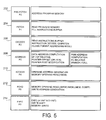
- the processor core 102 executes instructions through a 7 stage pipeline, the respective stages of which will now be described with reference to Figure 5.
- the first stage of the pipeline is a PRE-FETCH (P0) stage 202, during which stage a next program memory location is addressed by asserting an address on the address bus (PAB) 118 of a memory interface, or memory management unit 104.
- P0 PRE-FETCH
- PAB address bus
- FETCH (P1) stage 204 the program memory is read and the I Unit 106 is filled via the PB bus 122 from the memory management unit 104.
- the PRE-FETCH and FETCH stages are separate from the rest of the pipeline stages in that the pipeline can be interrupted during the PRE-FETCH and FETCH stages to break the sequential program flow and point to other instructions in the program memory, for example for a Branch instruction.
- the next instruction in the instruction buffer is then dispatched to the decoder/s 512/514 in the third stage, DECODE (P2) 206, where the instruction is decoded and dispatched to the execution unit for executing that instruction, for example to the P Unit 108, the A Unit 110 or the D Unit 112.
- the decode stage 206 includes decoding at least part of an instruction including a first part indicating the class of the instruction, a second part indicating the format of the instruction and a third part indicating an addressing mode for the instruction.
- the next stage is an ADDRESS (P3) stage 208, in which the address of the data to be used in the instruction is computed, or a new program address is computed should the instruction require a program branch or jump. Respective computations take place in the A Unit 110 or the P Unit 108 respectively.
- ADDRESS P3 stage 208
- an ACCESS (P4) stage 210 the address of a read operand is output and the memory operand, the address of which has been generated in a DAGEN X operator with an Xmem indirect addressing mode, is then READ from indirectly addressed X memory (Xmem).
- the next stage of the pipeline is the READ (P5) stage 212 in which a memory operand, the address of which has been generated in a DAGEN Y operator with an Ymem indirect addressing mode or in a DAGEN C operator with coefficient address mode, is READ.
- the address of the memory location to which the result of the instruction is to be written is output.
- read operands can also be generated in the Y path, and write operands in the X path.
- stage 214 there is an execution EXEC (P6) stage 214 in which the instruction is executed in either the A Unit 110 or the D Unit 112. The result is then stored in a data register or accumulator, or written to memory for Read/Modify/Write or store instructions. Additionally, shift operations are performed on data in accumulators during the EXEC stage.
- the present embodiment of the invention includes a memory management unit 104 which is coupled to external memory units via a 24 bit address bus 114 and a bi-directional 16 bit data bus 116. Additionally, the memory management unit 104 is coupled to program storage memory (not shown) via a 24 bit address bus 118 and a 32 bit bi-directional data bus 120. The memory management unit 104 is also coupled to the I Unit 106 of the machine processor core 102 via a 32 bit program read bus (PB) 122. The P Unit 108, A Unit 110 and D Unit 112 are coupled to the memory management unit 104 via data read and data write busses and corresponding address busses. The P Unit 108 is further coupled to a program address bus 128.
- PB program read bus
- the P Unit 108 is coupled to the memory management unit 104 by a 24 bit program address bus 128, the two 16 bit data write busses (EB, FB) 130, 132, and the two 16 bit data read busses (CB, DB) 134, 136.
- the A Unit 110 is coupled to the memory management unit 104 via two 24 bit data write address busses (EAB, FAB) 160, 162, the two 16 bit data write busses (EB, FB) 130, 132, the three data read address busses (BAB, CAB, DAB) 164, 166, 168 and the two 16 bit data read busses (CB, DB) 134, 136.
- the D Unit 112 is coupled to the memory management unit 104 via the two data write busses (EB, FB) 130, 132 and three data read busses (BB, CB, DB) 144, 134, 136.
- Figure 7 represents the passing of instructions from the I Unit 106 to the P Unit 108 at 124, for forwarding branch instructions for example. Additionally, Figure 7 represents the passing of data from the I Unit 106 to the A Unit 110 and the D Unit 112 at 126 and 128 respectively.
- MAC multiply and accumulate unit
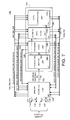
- FIG. 8 is a schematic overview of an embodiment of a MAC 300, corresponding to the MACs 42 and 44.
- Figure 8 shows that the MAC provides a network of cascaded sub-blocks:
- a partial product generation stage 324 which includes fractional mode control, receives first and second 17 bit operands 320 and 322 for generating partial products.
- the output of the partial products generation stage passes to a partial product summing tree 328, where rounding and partial multiplication saturation control are applied.
- a final adder stage 332 receives the 34 bit output of the partial product summing tree 328 and also a 40 bit Accumulator bus input (Ain).
- the final adder stage 332 includes zero and overflow flags detection, the flags being output at 334.
- a saturation stage 336 provides saturation to "0x007ffffffff” or “0x7ffffffff” or “0xff8000000” or “0x8000000000” and outputs a 40 bit result and provides 16 LSBs cleared for rounding.
- Control inputs 326 control the detailed operation of the MAC and control flags 334 are output by the decode unit.
- the partial product generation stage uses Booth encoding and the partial product reduction stages are implemented as a Wallace Tree structure. These techniques are described in "A suggestion for a fast multiplier” by CS Wallace, IEEE Transactions on Electronic Computers, 1964 and “A signed Binary Multiplication Technique", by Andrew D Booth, Quarterly Journal of mechanics and Applied Mathematics, Vol IV, part 2, 1951. More precisely, Radix-4 Booth encoding with a Wallace 4:2 based compressors reduction network is employed in the MAC 300.
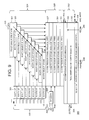
- Figure 9 shows the MAC 300 in more detail.
- the partial product generation stage 324 receives the X input 322 at fractional mode stage 323, and the Y input at Booth encoder stages 321. Also supplied as one input for the Booth stages is an Add/Subtract control signal (Add/sub). The partial products are then generated in a plurality of Booth select stages 325.
- the partial products are supplied to the partial product summing stage 328, which comprises a number of 3:2 Wallace tree compressor stages 327 and 4:2 Wallace tree compressor stages 331.
- Signals including Yin, Xin, and SMUL (saturation multiply) (or GSM) signals are supplied to a decoder 329, which applies a control signal to a compressor stage 327.
- a rounding (RND) control signal is also supplied to a compressor stage 327.
- the final adder stage 332 includes a 4:2 compressor stage 333 and the final adder itself 335.
- the compressor stage 333 receives the output of the last compressor stage 331.
- the 40 bit accumulator bus (Ain) is also effectively supplied to the adder 332, as are multiply/accumulate (Mpy/Acc) control signals. Zero and Overflow flags are output at 334 from the final adder 335.
- the final saturation stage 336 provides for 32/40 bits saturation and lowest significant bit clearing for rounding mode control.
- Saturation and rounding control signals (SAT, RND, RDM and OVF40) are supplied to the final saturation stage for rounding control).
- the 40 bit result Aout is output at 338.
- the Booth encoder stages 321 are implemented as a classical Booth encoder for dividing the number of partial products to be added.
- a Radix-4 encoder implements a modified Booth algorithm with 3 bits of a multiplier operand being converted to control zero Partial Product (PP) generation, multiplicand operand PP generation, multiplicand shifted by one position to the MSBs, PP generation and sign generation.
- Figure 10 is a table representing the Booth encoder, where p2, pl and sg are outputs.
- the Booth encoder basic equations should be packaged in one so-called leaf cell within the encoder. Output buffering can be left out of this cell. Nine cells like this are required to encode the 17 bits of the multiplier operand. Bits are associated in the manner indicated below:
- stage 325 It is in the partial product selection stages 325 that the partial products that will be further added together are generated.
- the stage consist of a multiplexor controlled by the signals "p2", “p1 " and “sg" previously described.
- Figure 12 is a Table describing a leaf cell that generates one bit of the partial product (PP).
- the first partial product also includes fractional mode control, as will be described later.
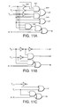
- Figure 13 shows the logic of the leaf cells.
- Figure 13A represents a normal stage.
- Figure 13B represents a normal stage with sign extension.
- Figure 13C represents a final stage, and
- Figure 13D a final stage with sign extension. It will be noted that the final stages are simpler than the normal stages.
- a compressor is an operator that adds together n partial product bits delivering a sum and a carry, bit.
- a 3:2 compressor sums 3 bits and delivers the two bits which are further reduced in the tree.
- a 4:2 compressor adds 4 bits together with a carry input and generates two bits and a carry output to its neighbor.
- the total number of reduction stages is three. The first one consist of at worst, three slices of 3:2 compressors 317 that will generate three (sum, carry) pairs per partial product bit. These pairs are further reduced by two cascaded stages of 4:2 compressors 321, finally delivering a (sum, carry) pair per partial product bit to be added in the accumulator 323.
- Figure 14 shows the partial products alignment and reduction using the first stage of compressors 327. Sign extension overhead in number of compressors is limited via addition of ones. Booth carries are also added in this stage (b0 to b8 signals). Rounding is performed by adding a one at bit position 15 when "RND" signal is active.
- Figure 15 is a logic diagram of a cell for a 4:2 Wallace compressor stage.
- This cell provides a 4:2 counter with a faster path from an input 'Pi' to an output 'Sum' and balanced paths from an input 'Cin' and an output 'Cout' and the input 'Pi' to the output 'Co'.
- the connection of the 4:2 compressor in the partial product reduction stage is in both horizontal (C0 - C1) and vertical directions (Sum; Cout - Pi).
- a particular application of the present embodiment is in digital telecommunications devices such as GSM devices.
- GSM requires the saturation and fractional mode control. In this embodiment, this is achieved by shifting the Xin operand by one position towards the most significant bit. This is implemented via a 2-input multiplexor as illustrated in Figure 16.
- the SMUL saturation mode implies that if "x1800" multiplied by "x1800” appears, the result must be forced to "007fffffff" or "0080007fff" where a rounding mode is selected.
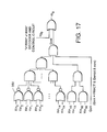
- Decoding of the Xin and Yin special operands is performed through standard logic gates as illustrated in Figure 17. (As mentioned above with reference to Figure 11A, symbol 350 represents a NOR gate). The result complements the Booth carry of the first stage in order to add all ones for the first partial product. The total decode time is not longer than the delay through the Booth encoding and partial product selection stages.
- the final adder stage includes addition of the accumulator content and sums and carries reduction. These operations are performed through a stage of 3:2 compressors in order to reduce the accumulator in (Ain), sum and carry busses to a new set of sums and carries, and an 40 bit adder to get the final result which is analyzed for 32 bits saturation detection.
- CLA Carry Look Ahead
- a one block CLA for 40 bits leads to a carry propagation scheme of a 64 bit adder, as regards both speed and area.
- Another technique based on the observation of the partial product reduction tree delay profile, allows pure CLA implementation to be limited to lower bits up to the bit position where this delay starts to decrease.
- the carry propagation effect is reduced by choosing a carry select adder scheme where the selection is performed by the carry output of the first CLA adder.
- a delay arrival profile can be taken into account by propagating the carry with a variable carry skip. This has the advantage of reducing toggling on the higher bits of the adder while getting a smaller CLA structure.
- Figure 18 depicts the delay arrival profile for the partial product reduction, in terms of elementary full adder delays, and the corresponding final adder structure.
- Zero detection it is noted that when the final result, at the adder output, is zero the corresponding flag (zero detector) is set to one. If rounding mode is active, the 16 least significant bits of the result are assumed to be zero for updating the flag. As such, conventional implementations that scan the final result bits (after rounding) lead to a unacceptable increase of the total MAC critical path.
- a zero anticipation mechanism or "Zero Result Anticipation” (ZRA) mechanism, is used to update the flag in parallel with the final addition.
- a slice of an operand comprises a range of bits of the operand.
- the degree of freedom provided by the index k in the above equation is used to slice the operand in the most efficient way, in terms of propagation delay. This is done by minimizing the global propagation time through the fast carry generator.
- the representation " ⁇ (a(i) + b(i))” indicates the complement of "(a(i) + b(i))"
- Z(i,0) ZERO(i,0) + G(i,0) + P(i,0)
- an operator is defined with the same properties as the operator "o". This can be derived from the equation (13) above. Indeed, two operand slices (n,k+1) and (k,m) each result in a zero if they have the property described in equation (13) above. A zero will be detected on a slice (n, m) in the two following cases: the state of the (k,m) slice is all zeros (A) the state of (n,k+1) is a zero_detect (i.e. the same as one of the states at (12)) (B) or the state of (k,m) is a zero_detect and the slice contains a "g" (C) the state of (n,k+1) is all p's (D)
- the G(i,j) and P(i,j) terms can be taken from the adder fast-carry generation intermediate results.
- cells can be created that are optimized both for layout implementation and performance. These cells are optimized for CMOS technology which invert signals.
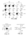
- Figure 20A is a schematic representation of an approach to implementing a zero anticipation mechanism in the form of time optimal adder comprising a binary tree of nodes N based on the principles set down in the above equations.
- the arrows A joining the nodes represent the propagation of intermediate zero signals.
- Figure 20A illustrates this structure for 8 bit positions B0 - B7. However, it will be apparent from Figure 20A how this can be extended to any number of bit positions.
- Figure 20B is a specific exemplary implementation for such a time optimal adder for 5 bits (e.g. bits B0 - B4 of Figure 20A).
- This includes an array of cells C(i,j), with cells CC, implementing the operator "u" for combining intermediate anticipation signal, and cells CB for forwarding intermediate anticipation signals between the cells CC.
- slice boundaries i,j
- a slice boundary is the boundary between slices.
- Each column in Figure 20B represents a bit position with the bit positions increasing from a lowest significant bit position on the right to successively higher bit positions towards the left.
- Inputs for bits B0 - B4 are supplied to cells of the first row 412.
- the intermediate anticipation signals ripple upwards through the second row 413 and the third row 414 and towards the left as indicated by the arrows.
- the signals pass from one row to the next with a delay corresponding to the time taken for the combining of the intermediate results, but pass horizontally without delay.
- the intermediate anticipation result from the first 2-bit operation 408 is generated at the cell 415 and is supplied to the third row 414 of cells of the three bit operation to form the global result at a vertical output from the cell 416.
- the principles employed correspond to those employed in the binary tree of Figure 20A.
- the first row 412 in Figure 20B corresponds to row R1 in Figure 20A.
- the cells CC of Figure 20B effectively correspond to the nodes N of Figure 20A. It will be noted that the distribution of the cells CC in the columns for bits B2, B3 and B4 and the rows 413 and 414 of Figure 20B differs from that of the nodes N in the columns for bits B2, B3 and B4 and the rows R2 and R3 of Figure 20A. This is due to the slicing of the 5-bit adder array of Figure 20B into the 2 bit and 3 bit sub-arrays 408 and 410.
- the final result of the zero detection can be supplied to enable anticipation of a zero result and to provide early indication of the result of, for example, condition codes evaluation.
- Figure 21 illustrates the inputs and outputs for one of the cells CC(i,j) 420 which are shown as a closed box in the Figure 20.
- This type of cell implements the "u" operation, and, in the general case, has the following inputs and outputs, both vertically and horizontally:
- a horizontal input 424 (if present) is simply passed to the horizontal output 426. This is performed without modification and without delay, so that the output signal is available substantially at the time the input signal is available.
- the vertical output 428 is a combination, as defined by the operator "u" of the vertical input 422 and the horizontal input 424. This process does take a certain time, so that the-vertical output 428 is available shortly after the vertical and horizontal inputs 422, 424 are available.
- the individual cells need not have a full set of inputs and outputs depending upon its position in the array, as shown in Figure 20.
- Figure 22 illustrates the inputs and outputs for one of the cells CB(i,j) 430 which are shown as an open box in Figure 20. This type of cell simply forwards signals from inputs to outputs of the cells, as illustrated below:
- the horizontal output signals (p_l, g_l, z_l) at 436 are copies of the vertical input signals (p_r, g_r, z_r) from 432, which have been "amplified” by a buffer.
- the vertical output signals (p_r, g_r,z_r) at 438 are the vertical input signals (p_r, g_r, z_r) from 432, which have been "amplified” by a buffer.
- a vertical input 432, if present, is passed to the horizontal and vertical outputs, 436 and 438 although the output is delayed with respect to the input by an amount corresponding to the delay involved in generating a combination signal in one of the combining cells CC 420.
- the individual cells CB 430 have vertical inputs and horizontal and/or vertical outputs depending upon the position in the array, as shown in Figure 20.
- the delay in the vertical direction provided by the buffer cells is needed in order that propagation of the signals in the upward direction in Figure 20B runs in parallel in each column.
- the horizontal propagation is effectively immediate, so that a result is available at the vertical output (where provided) of the last cell in the vertical direction (i.e. the topmost cell as shown in Figure 20B) for each bit position.
- the example shown in Figure 20B is effectively split into two sub-arrays, with intermediate anticipation signals propagating to the left and upwardly via the various cells in each sub-array, with the output of the first sub-array being combined with the output of the second cell in the third row (i.e. the topmost row of cells).
- the intermediate zero anticipation detection results which are available for the various bit positions in the top row of cells, are not needed.
- the top left cell alone in Figure 20, cell CC(4,0)
- cell CC(4,0) can be kept as an "u” operator, with one or more of the remaining cells in that row (where the intermediate results are not needed) being replaced by "o" operators, so as to avoid unnecessary logic and improve overall performance.
- "u" operator cells can also be provided at specific bit positions where intermediate zero anticipation results are needed for intermediate bit positions in an embodiment.
- Figure 23 is a schematic block diagram of an example of circuitry 450 including logic gates for implementing the "u" operator in one of the "CC" cells 420 of Figure 21.
- the inputs 422 and 424 shown in Figure 21 are provided at the left side of the Figure, and the outputs 426 and 428 are shown at the right hand side.
- the circuitry for the operator includes one NOT gate 452, four AND gates 454 and two OR gates 456. It can be seen that the gates implement the operator "u”. It will, however, be appreciated that other gate structures could be used to implement the operator "u” in other embodiments.
- Figure 24 is a schematic block diagram of an example of circuitry 460 for implementing one of the buffer cells CB of Figure 22.
- the vertical inputs 432 shown in Figure 24 are provided at the left hand side of the Figure and the horizontal and vertical outputs 436 and 438 are shown at the right hand side.
- the circuitry includes three buffer (delay) circuits 434, one for each of the g_r,p_r and z_r inputs 432.
- the delay factor of the buffer circuits is selected to match the delay imposed by the circuitry for performing the "u" operation.
- the outputs from the buffer circuits 434 are supplied to the horizontal and/or vertical outputs 436 and 438, depending on the position of the buffer cell CB in the array illustrated in Figure 20.
- Figure 25 is a schematic block diagram of an example application of the zero look-ahead mechanism of Figures 20A/20B to a forty-bit final adder stage 470 of a multiply and accumulate unit, such as the MACs 1 and 2 (42,44) shown in Figure 3.
- zero anticipation is required at forty bits and also at sixteen bits.
- a first zero anticipation stage 472 provides a zero anticipation output based on 16 bits B0-B15 supplied to it. These sixteen bits B0-B15 for which signals are supplied correspond to the sixteen lowest order bits of the arithmetic unit result.
- the arithmetic result bits are also supplied to the saturation stage 476 of the MAC.
- the zero anticipation result signal 473 on 16 bits is output at 477.
- a logical AND gate 478 where the signal is added to a partial zero anticipation result signal 475 from a second zero anticipation stage 474.
- the second zero anticipation stage 474 provides a zero anticipation output based on signals for 24 bits supplied to it.
- the twenty four bits for which signals are supplied correspond to the twenty four highest order bits B16-B39 of the forty bit arithmetic unit result.
- the arithmetic result bits B16-B39 are also supplied to the final adder stage 335 of the MAC, the output of the final adder stage comprising the product Pr.
- a global zero anticipation result signal 479 on 40 bits can be generated at the output of the AND gate 478.
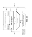
- Figure 26 illustrates in more detail the connection of the zero anticipation mechanism of Figure 25 in a MAC (e.g. the MAC 42 or the MAC 44 of Figure 3).
- the outputs from a partial product reduction tree 480 of the MAC is supplied to the forty bit final adder and zero anticipation mechanism 470.
- the outputs of the final adder and zero anticipation mechanism comprise the global zero anticipation flag 479 for the final result on forty bits, the result of the final adder 482 and the 16th bit zero anticipation flag 477.
- the results from the final adder 482 and the 16th bit zero anticipation flag 477 are supplied to the saturation stage 476 of the MAC, from which the output 483 is supplied to an accumulator register .
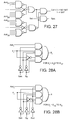
- Figure 27 illustrates an example of 32 bit saturation detection logic of the decoding section that generates the overflow bit OVF and also a saturation bit SATC which is a function of a saturation control signal SAT, causing a saturation mode and the presence of the overflow bit OVF.
- Overflow for extension bits is defined by the fact that Add[39:31] is either different from “0x1ff” or "0x000". The clamp value is then chosen based on the sign (Add[39]). If the RND signal is at one, Add[15:0] is set to "0x0000", in all cases.
- a cell is provided to generate the different values. There are two basic versions of this cell, one for bit positions lower than bit 15 and one for bit positions higher than bit 16. A special cell is provided for bits 16 to enable an unbiased rounding mode. If an unbiased rounding mode were not provided, the cell for bit 16 could be of the same type as for bit positions higher than 16. The various cell, which are described below, effectively define a multiplexor for selecting signals for the final accumulator.
- Figures 28A illustrates an example of a saturation control cell (multiplexor cell) suitable for each of bits X39 to X17.
- the signal ADD i is the bit to be added for the bit position i.
- the signal SG is bit is the sign bit represented by the ADD i bit for position 39 (i.e. ADD 39 ).
- the signal SATC is the saturation bit generated by the saturation detection logic of Figure 27.
- the signal Fi is set to one or zero depending on the cell position.
- Figure 28B illustrates an example of a saturation control cell (multiplexor cell) suitable for each of bits 15 to 0.
- the signal RND is a rounding signal. When this is active, rounding is effected on bits 15:0.
- Figure 28C illustrates an example of a saturation control cell (multiplexor cell) suitable for bit position 16.
- the signal UR is an unbiased rounding signal. This is generated when the zero anticipation signal Z16 477, from Figure 25 is active, representative of a zero having been detected for bits 15:0 (i.e. the first 16 bits) and a signal URM is active indicative of an unbiased rounding mode being active. The effect of this signal UR is to invalidate the Addi part of the multiplexor because saturation takes precedence over unbiased rounding.
- a rounded result which overflows e.g., for 32 bits, is represented as 7fff0000 and not 7ffe0000, and bit position 16 (i.e. the 17th bit) of the final adder is set to zero.
- the output of the AND gate 362 forming the signal UR will be low.
- the inverted UR signal from the NOT gate 364, i.e. the NUR signal, is then high, whereby, the NUR signal does not dominate the AND gate 366.
- the setting of bit X16 is controlled according to the saturation mode in the same manner as for bits X39 to X17. It will be appreciated that without the signal NUR, and the circuitry for generating that signal, the cell for bit position X16 corresponds to that for bit positions X39 to X17.
- zero anticipation is performed on a propagation tree of a carry lookahead structure.
- This uses the carry and sum generated from the partial product reduction tree 314. From the carry and sum, a zero result for the bit X16 is anticipated by mapping the propagation tree onto the one-zero result of the first 16 bits. This provides a propagation speed at least as fast as the carry propagation on the final adder. From the zero result, we can predict whether bit X16 of the MAC structure has to be forced to zero or not.
- Figure 30 illustrates logic for detecting an overflow on 40 bits.
- a control bit ovf4O enables an overflow on 32 bits if it is off, or an overflow on 40 bits if it is on. This detection occurs in a final 8 bits adder.
- a 40 bit overflow will occur if S[39] is different from S[40].
- OVF overflow
- OVF is directly derived with 2 XOR gates.
- the final result is forced to 0x7ffffffff or 0x8000000000 if the saturation signal (ovm) is on.
- Figure 31 is a schematic representation of an integrated circuit 40 incorporating the invention.
- the integrated circuit includes a plurality of contacts 42 for surface mounting.
- the integrated circuit could include other configurations, for example a plurality of pins on a lower surface of the circuit for mounting in a zero insertion force socket, or indeed any other suitable configuration.
- a processing engine such as the processor 10, for example as incorporated in an integrated circuit as in Figure 31, is in a telecommunications device, for example a mobile wireless telecommunications device.
- Figure 32 illustrates one example of such a telecommunications device.
- the telecommunications device is a mobile telephone 11 with integrated user input device such as a keypad, or keyboard 12 and a display 14.
- the display could be implemented using appropriate technology, as, for example, a liquid crystal display or a TFT display.
- the processor 10 is connected to the keypad 12, where appropriate via a keyboard adapter (not shown), to the display 14, where appropriate via a display adapter (not shown), and to a telecommunications interface or transceiver 16, for example a wireless telecommunications interface including radio frequency (RF) circuitry.
- the radio frequency circuitry could be incorporated into, or separate from, an integrated circuit 40 comprising the processor 10.
- the RF circuitry 16 is connected to an aerial 18.
- unbiased rounding is effected by forcing bit 16 to a predetermined value, here logical zero, when bits 15-0 are anticipated as being zero. It will be appreciated that this is one specific example. More generally, the (N + 1)th bit could be forced to that logical value when bits N - 0 are anticipated as being zero. Also, this description has been given specifically with respect to a multiply and accumulate (MAC) unit of a processor. However, the invention is not limited thereto and finds general application to arithmetic units of processing engines.
- MAC multiply and accumulate
Landscapes
- Engineering & Computer Science (AREA)
- Physics & Mathematics (AREA)
- General Physics & Mathematics (AREA)
- Theoretical Computer Science (AREA)
- Computational Mathematics (AREA)
- Computing Systems (AREA)
- Mathematical Analysis (AREA)
- Mathematical Optimization (AREA)
- Pure & Applied Mathematics (AREA)
- General Engineering & Computer Science (AREA)
- Executing Machine-Instructions (AREA)
- Complex Calculations (AREA)
Abstract
Description
- '0', Y0, Y1
- first encoder,
- Y1, Y2, Y3
- second encoder,
- Y3, Y4, Y5
- third encoder,
- ..., Y13, Y14, Y15
- eighth encoder.
- Y15, Y16
- ninth encoder.
| A | B | a + b + 1 | |
| sum | carry | ||
| 0 | 0 | 1 | 0 |
| 0 | 1 | 0 | 1 |
| 1 | 0 | 0 | 1 |
| 1 | 1 | 1 | 1 |

- ZERO(i,0) =
- State zero (402)
- G(i,0) =
- State generate (404)
- P(i,0) =
- State propagate (406).
the state of the (k,m) slice is all zeros (A)
the state of (n,k+1) is a zero_detect (i.e. the same as one of the states at (12)) (B)
or
the state of (k,m) is a zero_detect and the slice contains a "g" (C)
the state of (n,k+1) is all p's (D)


- Vertical input (422):
- p_r, g_r, z_r
- Horizontal input (424):
- p_l, g_l, z_l
- Horizontal output (426):
- p_l, g_l, z_l
- Vertical output (428):
- P, G, Z = (p_r,g_r,z_r)u(p_l,g_l,z_l)
- Vertical input (432):
- p_r, g_r, z_r
- Horizontal output (436) :
- p_l, g_l, z_l = p_r, g_r, z_r
- Vertical output(438):
- p_r, g_r, z_r
| A | 1 | 1 | 0 | 0 | 1 |
| B | 0 | 0 | 1 | 1 | 1 |
| p_in | 1 | 1 | 1 | 1 | 0 |
| g_in | 0 | 0 | 0 | 0 | 1 |
| z_in | 0 | 0 | 0 | 0 | 1 |
| stage 1 | P (4,4) = 1 | P (3,2) = 1 | P (2,2) = 1 | P (1,0)=0 | P (0,0) = 0 |
| G (4,4) = 0 | G (3,2) = 0 | G (2,2) = 0 | G (1,0) = 1 | G (0,0) = 1 | |
| Z (4,4) = 0 | Z (3,2) = 0 | Z (2,2) = 0 | Z (1,0)= 1 | Z (0,0) = 1 | |
| stage 2 | P (4,2) = 1 | P (3,2) = 1 | P (2,2) = 1 | P (1,0)=0 | P (0,0) = 0 |
| G (4,2) = 0 | G (3,2) = 0 | G (2,2) = 0 | G (1,0)=1 | G (0,0) = 1 | |
| Z (4,2) = 0 | Z (3,2) = 0 | Z (2,2) = 0 | Z (1,0) = 1 | Z (0,0) = 1 | |
| stage 3 | P (4,0) = 0 | P (3,0) = 0 | P (2,0) = 0 | P (1,0)=0 | P (0,0) = 0 |
| G (4,0) = 1 | G (3,0) = 1 | G (2,0) = 1 | G (1,0)=1 1 | G (0,0) = 1 | |
| Z (4,0) = 1 | Z (3,0) = 1 | Z (2,0) = 1 | Z (1,0)= 1 1 | Z (0,0) = 1 | |
| sum | 0 | 0 | 0 | 0 | 0 |
| zero | 1 | 1 | 1 | 1 | 1 |
S40 = A39^A39^C39 = C39
S39 = A39^ A38^C38, where A39 means the inverse of the A39 signal.
OVF = S40^S39
OVF = C39^A39^A38^C38
Claims (26)
- An arithmetic unit for a processing engine, the arithmetic unit comprising:arithmetic logic for performing an arithmetic operation to generate an arithmetic result;zero anticipation logic for anticipating a logical zero on N least significant bits of the result; andunbiased rounding logic for forcing a predetermined logic value on the (N+1)th least significant bit of the result.
- An arithmetic unit according to claim 1, wherein the predetermined logical value is logical zero.
- An arithmetic unit according to claim 1 or claim 2, wherein the zero anticipation tree comprises a carry propagation tree responsive to carry results of the arithmetic logic for anticipating a zero on each of N least significant bits of an arithmetic result to generate an output signal, the unbiased rounding logic being responsive to the output signal for forcing the (N+1)th least significant bit of the result to logical zero where a logic zero is anticipated on N lowest significant bits of the result.
- An arithmetic unit according to any preceding claim, wherein the unbiased rounding logic is selectively operable to provide unbiased rounding.
- An arithmetic unit according to any preceding claim, wherein the unbiased rounding logic comprises a multiplexor responsive to an unbiased rounding select signal selectively to enable forcing of the (N+1)th bit to logical zero.
- An arithmetic unit according to any preceding claim, wherein the arithmetic unit is a multiply and accumulate unit comprising a partial product reduction tree providing carry results, a final adder connected to the partial production reduction tree holding the result.
- An arithmetic unit according to claim 6, wherein the multiply and accumulate unit provides X-by-Y bit multiplication with accumulation on M bits.
- An arithmetic unit according to claim 7, where X = Y = 17 and M = 40.
- An arithmetic unit according to any preceding claim, wherein N is 16.
- An arithmetic unit according to any preceding claim, wherein said zero result anticipation logic generates a further output signal where all the bits of the result, or a predetermined number greater than N of least significant bits, are all logical zero.
- An arithmetic unit according to any preceding claim, wherein the arithmetic unit is a floating point unit with rounding to a nearest sticky bit.
- An arithmetic unit according to any one of claims 1 to 10, wherein the arithmetic unit is a fixed point unit with overflow anticipation.
- A processing engine comprising at least one arithmetic unit according to any preceding claim.
- A processing engine according to claim 14 in the form of a digital signal processor.
- An integrated circuit comprising a processing engine according to claim 13 or claim 14.
- Telecommunications apparatus comprising a processing engine according to claim 13 or claim 14.
- Telecommunications apparatus according to claim 16, comprising a user input device, a display, a wireless telecommunications interface and an aerial.
- A method for unbiased rounding in an arithmetic unit of a processing engine, the method comprising:performing an arithmetic operation to generate an arithmetic result;anticipating a logical zero on N least significant bits of the result; andforcing a predetemined logical value on the (N+1)th least significant bit of the result where a logic zero is anticipated on N least significant bits of the result.
- A method according to claim 18, wherein the predetermined logical value is logical zero.
- A method according to claim 18 or claim 19, wherein zero anticipation is effected by performing carry propagation in a carry propagation tree in response to carry results of arithmetic logic and generating an output signal where a logical zero is anticipated on N least significant bits of the result.
- A method according to claim 20, comprising selectively supplying an unbiased rounding select signal selectively to enable forcing of the (N+1)th bit to zero when a logical zero is anticipated for N lowest significant bits.
- A method according to any one of claims 18 to 21, wherein the arithmetic unit is a multiply and accumulate unit comprising a partial product reduction tree providing carry results, a final adder connected to the partial production reduction tree holding the result.
- A method according to claim 22, wherein the multiply and accumulate unit provides X-by-Y bit multiplication with accumulation on M bits
- A method according to claim 23, where X = Y = 17 and M = 40.
- A method according to any one of claims 18 to 24, wherein N is 16.
- A method according to any one of claims 18 to 25, additionally generating an zero anticipation result output where all the bits of the result, or a predetermined number greater than N of least significant bits, are all anticipated to be logical zero.
Priority Applications (3)
| Application Number | Priority Date | Filing Date | Title |
|---|---|---|---|
| DE1998624000 DE69824000T2 (en) | 1998-10-06 | 1998-10-06 | rounding mechanism |
| EP19980402458 EP0992883B1 (en) | 1998-10-06 | 1998-10-06 | Rounding mechanism |
| US09/411,186 US7047272B2 (en) | 1998-10-06 | 1999-10-01 | Rounding mechanisms in processors |
Applications Claiming Priority (1)
| Application Number | Priority Date | Filing Date | Title |
|---|---|---|---|
| EP19980402458 EP0992883B1 (en) | 1998-10-06 | 1998-10-06 | Rounding mechanism |
Publications (2)
| Publication Number | Publication Date |
|---|---|
| EP0992883A1 true EP0992883A1 (en) | 2000-04-12 |
| EP0992883B1 EP0992883B1 (en) | 2004-05-19 |
Family
ID=8235515
Family Applications (1)
| Application Number | Title | Priority Date | Filing Date |
|---|---|---|---|
| EP19980402458 Expired - Lifetime EP0992883B1 (en) | 1998-10-06 | 1998-10-06 | Rounding mechanism |
Country Status (2)
| Country | Link |
|---|---|
| EP (1) | EP0992883B1 (en) |
| DE (1) | DE69824000T2 (en) |
Cited By (1)
| Publication number | Priority date | Publication date | Assignee | Title |
|---|---|---|---|---|
| EP3035188A1 (en) * | 2014-11-25 | 2016-06-22 | AptCore Ltd | Fixed-point multiplication by one |
Citations (2)
| Publication number | Priority date | Publication date | Assignee | Title |
|---|---|---|---|---|
| EP0469841A1 (en) * | 1990-07-30 | 1992-02-05 | Matsushita Electric Industrial Co., Ltd. | Data round-off device |
| US5128889A (en) * | 1990-02-22 | 1992-07-07 | Matsushita Electric Industrial Co., Ltd. | Floating-point arithmetic apparatus with compensation for mantissa truncation |
-
1998
- 1998-10-06 DE DE1998624000 patent/DE69824000T2/en not_active Expired - Lifetime
- 1998-10-06 EP EP19980402458 patent/EP0992883B1/en not_active Expired - Lifetime
Patent Citations (2)
| Publication number | Priority date | Publication date | Assignee | Title |
|---|---|---|---|---|
| US5128889A (en) * | 1990-02-22 | 1992-07-07 | Matsushita Electric Industrial Co., Ltd. | Floating-point arithmetic apparatus with compensation for mantissa truncation |
| EP0469841A1 (en) * | 1990-07-30 | 1992-02-05 | Matsushita Electric Industrial Co., Ltd. | Data round-off device |
Non-Patent Citations (2)
| Title |
|---|
| HILLMAN G D: "DSP56200: AN ALGORITHM-SPECIFIC DIGITAL SIGNAL PROCESSOR PERIPHERAL", PROCEEDINGS OF THE IEEE, vol. 75, no. 9, September 1987 (1987-09-01), pages 1185 - 1191, XP000031791 * |
| R. OWEN: "A SUB 10 NANOSECOND MULTIPLIER AND MULTIPLIER-ACCUMULATOR", WESCON CONVENTION RECORD., vol. 30, 18 November 1986 (1986-11-18) - 20 November 1986 (1986-11-20), NORTH HOLLYWOOD US, pages 14/5 1 - 5, XP002093109 * |
Cited By (1)
| Publication number | Priority date | Publication date | Assignee | Title |
|---|---|---|---|---|
| EP3035188A1 (en) * | 2014-11-25 | 2016-06-22 | AptCore Ltd | Fixed-point multiplication by one |
Also Published As
| Publication number | Publication date |
|---|---|
| EP0992883B1 (en) | 2004-05-19 |
| DE69824000D1 (en) | 2004-06-24 |
| DE69824000T2 (en) | 2005-06-09 |
Similar Documents
| Publication | Publication Date | Title |
|---|---|---|
| US7047272B2 (en) | Rounding mechanisms in processors | |
| EP0992885B1 (en) | Multiplier accumulator circuits | |
| US6571268B1 (en) | Multiplier accumulator circuits | |
| US5448509A (en) | Efficient hardware handling of positive and negative overflow resulting from arithmetic operations | |
| US6381625B2 (en) | Method and apparatus for calculating a power of an operand | |
| US6282556B1 (en) | High performance pipelined data path for a media processor | |
| JP2662196B2 (en) | Calculation result normalization method and apparatus | |
| US8341204B2 (en) | Vector SIMD processor | |
| US6269384B1 (en) | Method and apparatus for rounding and normalizing results within a multiplier | |
| US6134574A (en) | Method and apparatus for achieving higher frequencies of exactly rounded results | |
| US20060041610A1 (en) | Processor having parallel vector multiply and reduce operations with sequential semantics | |
| US20050071413A1 (en) | Processor reduction unit for accumulation of multiple operands with or without saturation | |
| JP5719341B2 (en) | Mechanism for fast detection of overshifts in floating point units | |
| US6115733A (en) | Method and apparatus for calculating reciprocals and reciprocal square roots | |
| US5301139A (en) | Shifter circuit for multiple precision division | |
| US7519646B2 (en) | Reconfigurable SIMD vector processing system | |
| EP0992883B1 (en) | Rounding mechanism | |
| JP3579087B2 (en) | Arithmetic unit and microprocessor | |
| US6393554B1 (en) | Method and apparatus for performing vector and scalar multiplication and calculating rounded products | |
| EP0992917B1 (en) | Linear vector computation | |
| EP0992884B1 (en) | Zero anticipation method and apparatus | |
| US6487576B1 (en) | Zero anticipation method and apparatus | |
| Farooqui et al. | 64-bit media adder | |
| US6631393B1 (en) | Method and apparatus for speculative addition using a limited carry | |
| US20090063609A1 (en) | Static 4:2 Compressor with Fast Sum and Carryout |
Legal Events
| Date | Code | Title | Description |
|---|---|---|---|
| PUAI | Public reference made under article 153(3) epc to a published international application that has entered the european phase |
Free format text: ORIGINAL CODE: 0009012 |
|
| AK | Designated contracting states |
Kind code of ref document: A1 Designated state(s): DE FI FR GB SE |
|
| AX | Request for extension of the european patent |
Free format text: AL;LT;LV;MK;RO;SI |
|
| 17P | Request for examination filed |
Effective date: 20000825 |
|
| AKX | Designation fees paid |
Free format text: DE FI FR GB SE |
|
| RAP1 | Party data changed (applicant data changed or rights of an application transferred) |
Owner name: TEXAS INSTRUMENTS FRANCE Owner name: TEXAS INSTRUMENTS INC. |
|
| 17Q | First examination report despatched |
Effective date: 20020513 |
|
| GRAH | Despatch of communication of intention to grant a patent |
Free format text: ORIGINAL CODE: EPIDOS IGRA |
|
| GRAH | Despatch of communication of intention to grant a patent |
Free format text: ORIGINAL CODE: EPIDOS IGRA |
|
| GRAA | (expected) grant |
Free format text: ORIGINAL CODE: 0009210 |
|
| AK | Designated contracting states |
Kind code of ref document: B1 Designated state(s): DE FI FR GB SE |
|
| PG25 | Lapsed in a contracting state [announced via postgrant information from national office to epo] |
Ref country code: FI Free format text: LAPSE BECAUSE OF FAILURE TO SUBMIT A TRANSLATION OF THE DESCRIPTION OR TO PAY THE FEE WITHIN THE PRESCRIBED TIME-LIMIT Effective date: 20040519 |
|
| REG | Reference to a national code |
Ref country code: GB Ref legal event code: FG4D |
|
| REF | Corresponds to: |
Ref document number: 69824000 Country of ref document: DE Date of ref document: 20040624 Kind code of ref document: P |
|
| PG25 | Lapsed in a contracting state [announced via postgrant information from national office to epo] |
Ref country code: SE Free format text: LAPSE BECAUSE OF FAILURE TO SUBMIT A TRANSLATION OF THE DESCRIPTION OR TO PAY THE FEE WITHIN THE PRESCRIBED TIME-LIMIT Effective date: 20040819 |
|
| ET | Fr: translation filed | ||
| PLBE | No opposition filed within time limit |
Free format text: ORIGINAL CODE: 0009261 |
|
| STAA | Information on the status of an ep patent application or granted ep patent |
Free format text: STATUS: NO OPPOSITION FILED WITHIN TIME LIMIT |
|
| 26N | No opposition filed |
Effective date: 20050222 |
|
| REG | Reference to a national code |
Ref country code: FR Ref legal event code: PLFP Year of fee payment: 18 |
|
| PGFP | Annual fee paid to national office [announced via postgrant information from national office to epo] |
Ref country code: GB Payment date: 20150924 Year of fee payment: 18 |
|
| PGFP | Annual fee paid to national office [announced via postgrant information from national office to epo] |
Ref country code: FR Payment date: 20150924 Year of fee payment: 18 |
|
| PGFP | Annual fee paid to national office [announced via postgrant information from national office to epo] |
Ref country code: DE Payment date: 20151030 Year of fee payment: 18 |
|
| REG | Reference to a national code |
Ref country code: DE Ref legal event code: R119 Ref document number: 69824000 Country of ref document: DE |
|
| GBPC | Gb: european patent ceased through non-payment of renewal fee |
Effective date: 20161006 |
|
| REG | Reference to a national code |
Ref country code: FR Ref legal event code: ST Effective date: 20170630 |
|
| PG25 | Lapsed in a contracting state [announced via postgrant information from national office to epo] |
Ref country code: DE Free format text: LAPSE BECAUSE OF NON-PAYMENT OF DUE FEES Effective date: 20170503 Ref country code: FR Free format text: LAPSE BECAUSE OF NON-PAYMENT OF DUE FEES Effective date: 20161102 Ref country code: GB Free format text: LAPSE BECAUSE OF NON-PAYMENT OF DUE FEES Effective date: 20161006 |