EP0987907A2 - Telecommunication module having edge mounted jack and switch therefor - Google Patents
Telecommunication module having edge mounted jack and switch therefor Download PDFInfo
- Publication number
- EP0987907A2 EP0987907A2 EP99307322A EP99307322A EP0987907A2 EP 0987907 A2 EP0987907 A2 EP 0987907A2 EP 99307322 A EP99307322 A EP 99307322A EP 99307322 A EP99307322 A EP 99307322A EP 0987907 A2 EP0987907 A2 EP 0987907A2
- Authority
- EP
- European Patent Office
- Prior art keywords
- jack
- switch
- circuit board
- telecommunication
- operation shaft
- Prior art date
- Legal status (The legal status is an assumption and is not a legal conclusion. Google has not performed a legal analysis and makes no representation as to the accuracy of the status listed.)
- Withdrawn
Links
Images


Classifications
-
- H—ELECTRICITY
- H05—ELECTRIC TECHNIQUES NOT OTHERWISE PROVIDED FOR
- H05K—PRINTED CIRCUITS; CASINGS OR CONSTRUCTIONAL DETAILS OF ELECTRIC APPARATUS; MANUFACTURE OF ASSEMBLAGES OF ELECTRICAL COMPONENTS
- H05K7/00—Constructional details common to different types of electric apparatus
-
- H—ELECTRICITY
- H04—ELECTRIC COMMUNICATION TECHNIQUE
- H04Q—SELECTING
- H04Q3/00—Selecting arrangements
-
- H—ELECTRICITY
- H04—ELECTRIC COMMUNICATION TECHNIQUE
- H04Q—SELECTING
- H04Q1/00—Details of selecting apparatus or arrangements
- H04Q1/02—Constructional details
- H04Q1/14—Distribution frames
- H04Q1/142—Terminal blocks for distribution frames
-
- H—ELECTRICITY
- H04—ELECTRIC COMMUNICATION TECHNIQUE
- H04Q—SELECTING
- H04Q2201/00—Constructional details of selecting arrangements
- H04Q2201/12—Printed circuits
-
- Y—GENERAL TAGGING OF NEW TECHNOLOGICAL DEVELOPMENTS; GENERAL TAGGING OF CROSS-SECTIONAL TECHNOLOGIES SPANNING OVER SEVERAL SECTIONS OF THE IPC; TECHNICAL SUBJECTS COVERED BY FORMER USPC CROSS-REFERENCE ART COLLECTIONS [XRACs] AND DIGESTS
- Y10—TECHNICAL SUBJECTS COVERED BY FORMER USPC
- Y10S—TECHNICAL SUBJECTS COVERED BY FORMER USPC CROSS-REFERENCE ART COLLECTIONS [XRACs] AND DIGESTS
- Y10S439/00—Electrical connectors
- Y10S439/944—Coaxial connector having circuit-interrupting provision effected by mating or having "dead" contact activated after mating
Definitions
- the present invention relates to telecommunication switches and, in particular, the present invention relates to a telecommunication module such as a Digital Signal Cross Connect (DSX) module that has a jack mounted to an edge of a Printed Circuit Board (PCB) and a switch therefor.
- a telecommunication module such as a Digital Signal Cross Connect (DSX) module that has a jack mounted to an edge of a Printed Circuit Board (PCB) and a switch therefor.
- DSX Digital Signal Cross Connect
- PCB Printed Circuit Board
- Telecommunication modules such as DSX modules
- DSX modules are used as interfaces for cross connecting an electrical signal from one telecommunications device or network to another.
- each jack which is typically a WECO or BNC jack
- a switch which in turn is mounted on a PCB.
- current jacks are limited by their size, cost, and adaptability.
- current jacks have electrical power running through them when the associated DSX module is coupled to a backplane because switches contained within the module are normally open. Therefore, electrocution can occur if a conductive object, such as a pen or paperclip, is inserted into the jack.
- the jacks of present DSX modules are "live" without a plug inserted into the jacks.
- a telecommunication module for receiving a plug and having a circuit board disposed therein with a bounding edge, the telecommunication module comprising:
- a preferred feature of the present telecommunication module is that an angled ramp is coupled to the switch operation shaft and spaced apart from the switch.
- the jack may further include an opening disposed therein for receiving the angled ramp therein.
- a camshaft is preferably coupled to the switch operation shaft and is in axial alignment therewith for rotating when the switch operation shaft is rotated to change states of the switch.
- Each output and input jack preferably has two spaced apart openings for receiving the angled ramp therein such that the switch and the associated switch operation shaft can be mounted on either side of the jack on the circuit board.
- the switch preferably further includes a plurality of leaf springs mounted thereon and a corresponding plurality of L-shaped members against which the plurality of leaf springs are naturally biased.
- the camshaft includes a plurality of extensions for each releasing mechanical contact with one of the plurality of leaf springs thereby causing mechanical and electrical connection to be made between the plurality of L-shaped members and the plurality of leaf springs in axial alignment therewith.
- a rocker arm performs the function of the camshaft with extensions.
- the invention further provides a telecommunication jack for mounting on a circuit board having a bounding edge, two sides, and a plurality of pads attached thereto for electrical communication, the jack comprising:
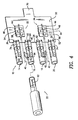
- FIG. 1 is a perspective view of a module of the present invention.
- FIG. 2 is a perspective view of the module of the present invention showing a plurality ofjacks mounted on an edge of a PCB of the module.
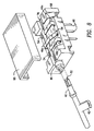
- FIG. 3 is a perspective view of the module of the present invention showing the plurality of jacks mounted on the edge of the PCB of the module with a plug being inserted into a jack of the module.
- FIG. 4 is a phantom view of the module of the present invention showing the plurality of jacks mounted on the edge of the PCB of the module with a plug being inserted into one of the jacks of the module.
- FIG. 5 is an exploded view of a first embodiment of a switch of the present invention.
- FIG. 6 is a side elevational view of the first embodiment of the switch of the present invention.
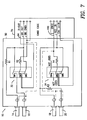
- FIG. 7 is a circuit schematic of the circuit board for the first embodiment and a second embodiment module of the present invention.
- FIG. 8 is a perspective view of the second embodiment of the switch of the present invention.
- FIG. 9 is a perspective view of one of the edge mountable jacks of the present invention.
- FIG. 10 is a front elevational view of the plurality of jacks of the module of the present invention.
- FIG. 1 Shown in FIG. 1 is a telecommunication module 10, such as a Digital Signal Cross Connect (DSX) module, which is typically releasably secured within a panel for allowing communication between a piece of telecommunications equipment and a telecommunications network, such as a telephone network.
- a telecommunication module such as a Digital Signal Cross Connect (DSX) module
- DSX Digital Signal Cross Connect
- the present module 10 receives a DS-3 signal, which is at a high frequency rate on the order of 44.736 megabits per second, but could be a lower frequency signal such as DS-1 on the order of 1.544 megabits per second or higher frequency signal such as a DS-4 on the order of 274.176 megabits per second.
- the module 10 includes a plastic casing 12 to protect the contents of the module 10.
- a tab 26 protrudes through the casing 12 for securing the module 10 within the panel.
- the module 10 has at least one jack such as a BNC for receiving a plug 22 therein, as shown in FIG. 3, but preferably has a plurality of WECO jacks including a first monitor jack 14, an output jack 16, an input jack 18, and a second monitor jack 20.
- the first monitor jack 14 and the second monitor jack 20 provide for the taking of samples of a signal from the telecommunications network and the output jack 16 and input jack 18 are for receiving the signal from, and inputting a signal to, the telecommunications network, respectively, as will be discussed in greater below.
- a Printed Circuit Board (PCB) 50 is disposed within the module 10 and has a bounding edge 28 to which the first monitor jack 14, the output jack 16, the input jack 18, and the second monitor jack 20 are coupled for receiving a plug 22 therein.
- Each of the jacks includes an integral pad 74 as is best shown in FIGS. 6 and 9, which has a plurality of legs 30 extending therefrom for being slidingly received about the circuit board 50 and preferably held in place via friction fit. It is understood, however, that the legs 30 could also be secured to PCB 50 in other ways such as being soldered to the PCB 50 or received within slots in the PCB 50.
- the legs 30 need be employed on the jack, and it can be attached by being soldered to the PCB 50 or received within a slot via friction fit.
- the coaxial rod 64 serves to hold the jack to the PCB 50 whether via friction fit, soldering, or being received within a slot.
- the legs 30 or leg also serve to hold the jack to the PCB 50 whether via friction fit, soldering, or being received within a slot. It is understood, however, that either the coaxial rod 64, the legs 30, or leg can hold the jack to the PCB 50.
- the legs 30 that are secured to the side of the PCB 50 on which the switches 32 and 34 are mounted, which will be discussed below, contact grounding pads 52, as shown in FIGS. 2, 3, and 4, which ground the PCB 50 to the jack.
- the pads 74 are mounted on the bounding edge 28 of the circuit board 50.
- the rod 64 of each of the jacks 14, 16, 18, and 20 projects outside the jacks, as is best shown in FIG. 9, and preferably contacts a landing pad 92 on the PCB 50 and is in electrical and mechanical communication therewith, which is shown in FIGS. 2, 3, and 4. It is also understood, however, that the rod 64 apart from friction contacting the landing pad 92, can also be soldered thereto or received within a port that contains an abutting or encircling landing pad 92.
- each rod 64 Surrounding each rod 64 is a solid, annular dielectric 72 preferably consisting of Teflon, which is manufactured by the DuPont Company of the United States.
- the dielectric 72 prevents any electro-magnetic frequencies existing on the rod 64 from transferring to the casing of the jack.
- the present telecommunication module 10 further includes at least one switch, but preferably includes a first switch 32 for the output jack 16 and second switch 34 for the input jack 18, as is best shown in FIGS. 2, 3, 4, and 7.
- Each switch 32, 34 has a first state and a second state, as will be discussed in greater detail below.
- each switch 32, 34 is mounted on the circuit board 50 via a plurality of prongs 68, which are inserted through apertures in the circuit board 50, and soldered thereto.
- the prongs 68 are coupled to a base 58 of each switch 32, 34, which is shown in FIG. 5.
- the base 58 is preferably constructed of a non-conductive material such as thermoplastic or nylon and has an elongated channel 48 formed lengthwise therein for receiving, at least partially, a rotatable camshaft 44 therein.
- the camshaft 44 is constructed of an electrically conductive metal such as steel or aluminum.
- each switch operation shaft 40 extends outward from the switches 32, 34 such that each switch operation shaft 40 is adjacent to one of the jacks 16, 18.
- Angled ramps 42 are coupled to the switch operation shafts 40 and spaced apart from the switches 32, 34.
- the camshaft 44 is in axial alignment with the switch operation shaft 40 for rotating when the switch operation shaft 40 is rotated to change states of each switch 32, 34.
- a card edge 70 is formed on the circuit board 50 for coupling to a card edge 70 connector.
- the card edge 70 has electrical contacts on only one side, as shown in FIG. 7, and is formed opposite the jacks 14, 16, 18, 20 on the circuit board 50, and will be discussed in greater detail below.
- an opening is disposed in each of the jacks, but preferably two spaced apart openings 66 for receiving the angled ramp 42 therein such that the switch and the associated switch operation shaft 40 can be mounted on either side of the jacks 14, 16, 18, 20 on the circuit board 50.
- the plug 22 When the plug 22 is inserted into one of the jacks 14, 16, 18, 20 the plug 22 contacts the angled ramp 42 within the jack causing the ramp 42 to be biased out of the jack through one of the openings 66 and thus the switch operation shaft 40 to rotate, thereby changing states of the switch from a normally closed state where an electrical signal does not enter the jack, to a state where it does.
- the switch 32 further includes a plurality of electrically conductive leaf springs 46 mounted to the base 58 and a corresponding and opposing plurality of electrically conductive L-shaped members 54 mounted in slots 52 formed in the base 58.
- the leaf springs 46 and L-shaped members 54 are preferably constructed of copper for electrical conductivity.
- a plastic cover 60 snap fits onto the base 58 and covers the L-shaped members 54, leaf springs 46, camshaft 44, slots 52, and base 58.
- the camshaft 44 includes a plurality of extensions 56 for allowing the switch 32 to have a first normally closed state with two of the extensions 56 releasing mechanical contact between two of the plurality of leaf springs 46b and 46c and two of the L-shaped members 54, in axial alignment therewith, when the plug 22 is not installed in the associated jack. This is accomplished by two of the extensions 56 actuated “under” the leaf springs 46b and 46c, thereby lifting the leaf springs 46b and 46c such that they do not contact the L-shaped members 54. Also in this normally closed state, the middle leaf spring 46a contacts one of the L-shaped members 54 that is in axial alignment therewith.
- FIG. 8 A second embodiment of the present switch 32 is shown in FIG. 8, the switch 32 further includes a plurality of electrically conductive leaf springs 46 mounted to the base 58 and a corresponding and opposing plurality of electrically conductive L-shaped members 54 mounted in slots 52 formed in the base 58.
- the leaf springs 46 and L-shaped members 54 are preferably constructed of copper for electrical conductivity.
- a rocker arm 78 is mounted via friction fit in the base 58 of this embodiment.
- Integrally coupled to the rocker arm 78 is a coupling cylinder 80 that has a cross-shaped aperture disposed therein for receiving a complimentary cross-shaped coupler attached to the switch operation shaft 40.
- a plastic cover 60 snap fits onto the base 58 and covers the L-shaped members 54, leaf springs 46, rocker arm 78, and base 58.
- the rocker arm 78 prevents mechanical contact between two of the plurality of leaf springs 46b and 46c and two of the L-shaped members 54, in axial alignment therewith, when the plug 22 is not installed in the associated jack. This is accomplished by the rocker arm 78 being placed "under” the leaf springs 46b and 46c, thereby lifting the leaf springs 46b and 46c such that they do not contact the L-shaped members 54. Also in this normally closed state, the middle leaf spring 46a contacts one of the L-shaped members 54 that is in axial alignment therewith.
- the telecommunications signal on the cross connect X-OUT line 94 and the cross connect X-IN line 104 on the card edge 70 to be routed to the signal OUT line 96 and signal IN line 102, respectively, when the plug 22 is not inserted into one of the jacks 16, 18.
- this provides for a normally closed circuit with the jacks normally open to prevent electrical shock unless the plug 22 is inserted therein and the associated DSX module is inserted into a panel whereby it is energized.
- a co-axial pin 62 of the plug 22 comes in electrical and mechanical communication with a co-axial rod 64 disposed in the output jack 16, as shown in FIG. 4.
- the co-axial rod 64 preferably has a bore disposed therein for receiving, at least partially, the co-axial pin 62 of the plug 22.
- one of the extensions 56 or rocker arm 78 will lift leaf spring 46a from contacting the L-shaped member 54 in axial alignment therewith. This occurs when the camshaft of switch 32 is rotated clockwise and represents the opening of switch SW3, as shown in FIG. 7, while simultaneously switches SW1 and SW2 become closed.
- the signal on the cross connect X-OUT line 94 will be routed across resistor R2, which preferably has a resistance of seventy-five ohms. The signal then continues to a first ground line 98.
- the signal on the OUT line is routed through switch SW1, because SW3 will be open circuited and the signal is received in the output jack 16.
- the signal on the OUT line 96 of the card edge 70 is sent across resistor R1, which has a preferred value of seven hundred and sixty-eight ohms. This relatively large resistance value allows approximately five percent of the signal to pass, which can then be monitored via the first monitor jack 14, and results in no degradation in performance of the telecommunications network.
- the signal on the IN line 102 is routed to the input jack 18.
- the signal on the IN line 102 of the card edge 70 is sent across resistor R3, which has a preferred value of seven hundred and sixty-eight ohms. This relatively large resistance value only allows approximately five percent of the signal to pass, which can then be monitored via the second monitor jack 20.
- resistor R3 has a preferred value of seven hundred and sixty-eight ohms. This relatively large resistance value only allows approximately five percent of the signal to pass, which can then be monitored via the second monitor jack 20.
- clockwise and “counterclockwise” used throughout are meant to be exemplary and could easily be reversed if switches 32 and 34 were reversed such that the switch operation shafts 40 are on opposite sides of the input and output jacks 18 and 16, respectively, than that shown in FIG. 4.
Landscapes
- Engineering & Computer Science (AREA)
- Computer Networks & Wireless Communication (AREA)
- Microelectronics & Electronic Packaging (AREA)
- Coupling Device And Connection With Printed Circuit (AREA)
- Details Of Connecting Devices For Male And Female Coupling (AREA)
- Connector Housings Or Holding Contact Members (AREA)
Abstract
Description
- In general, the present invention relates to telecommunication switches and, in particular, the present invention relates to a telecommunication module such as a Digital Signal Cross Connect (DSX) module that has a jack mounted to an edge of a Printed Circuit Board (PCB) and a switch therefor.
- Telecommunication modules, such as DSX modules, are used as interfaces for cross connecting an electrical signal from one telecommunications device or network to another. In current designs each jack, which is typically a WECO or BNC jack, of a DSX module is coupled to, and mounted on top of, a switch, which in turn is mounted on a PCB. This creates a thick housing for the module that encases the jacks, switches, and at least part of the PCB of the module. Thus, current jacks are limited by their size, cost, and adaptability.
- Moreover, current jacks have electrical power running through them when the associated DSX module is coupled to a backplane because switches contained within the module are normally open. Therefore, electrocution can occur if a conductive object, such as a pen or paperclip, is inserted into the jack. The jacks of present DSX modules are "live" without a plug inserted into the jacks.
- According to a first aspect of the invention, there is provided a telecommunication module for receiving a plug and having a circuit board disposed therein with a bounding edge, the telecommunication module comprising:
- a jack mounted on the circuit board for receiving the plug therein;
- a switch mounted on the circuit board and having at least two states;
- a switch operation shaft mechanically and electrically coupled to the switch and extending outward therefrom such that the switch operation shaft is adjacent to the jack; and
-
- A preferred feature of the present telecommunication module is that an angled ramp is coupled to the switch operation shaft and spaced apart from the switch. The jack may further include an opening disposed therein for receiving the angled ramp therein. When the plug is inserted into the jack, the plug contacts the angled ramp within the jack causing the switch operation shaft to rotate, thereby changing states of the switch as the angled ramp is biased from within the jack.
- A camshaft is preferably coupled to the switch operation shaft and is in axial alignment therewith for rotating when the switch operation shaft is rotated to change states of the switch. Each output and input jack, however, preferably has two spaced apart openings for receiving the angled ramp therein such that the switch and the associated switch operation shaft can be mounted on either side of the jack on the circuit board. The switch preferably further includes a plurality of leaf springs mounted thereon and a corresponding plurality of L-shaped members against which the plurality of leaf springs are naturally biased.
- In one embodiment, the camshaft includes a plurality of extensions for each releasing mechanical contact with one of the plurality of leaf springs thereby causing mechanical and electrical connection to be made between the plurality of L-shaped members and the plurality of leaf springs in axial alignment therewith. In another embodiment, a rocker arm performs the function of the camshaft with extensions.
- The invention further provides a telecommunication jack for mounting on a circuit board having a bounding edge, two sides, and a plurality of pads attached thereto for electrical communication, the jack comprising:
- a pad abutting the bounding edge of the circuit board;
- a dielectric secured in the pad;
- a holding structure projecting outside the jack and, in use, in electrical and mechanical communication with one of the plurality of pads of the circuit board; and
- attachment means for securing the jack to the circuit board.
-
- FIG. 1 is a perspective view of a module of the present invention.
- FIG. 2 is a perspective view of the module of the present invention showing a plurality ofjacks mounted on an edge of a PCB of the module.
- FIG. 3 is a perspective view of the module of the present invention showing the plurality of jacks mounted on the edge of the PCB of the module with a plug being inserted into a jack of the module.
- FIG. 4 is a phantom view of the module of the present invention showing the plurality of jacks mounted on the edge of the PCB of the module with a plug being inserted into one of the jacks of the module.
- FIG. 5 is an exploded view of a first embodiment of a switch of the present invention.
- FIG. 6 is a side elevational view of the first embodiment of the switch of the present invention.
- FIG. 7 is a circuit schematic of the circuit board for the first embodiment and a second embodiment module of the present invention.
- FIG. 8 is a perspective view of the second embodiment of the switch of the present invention.
- FIG. 9 is a perspective view of one of the edge mountable jacks of the present invention.
- FIG. 10 is a front elevational view of the plurality of jacks of the module of the present invention.
- The above and other features, aspects, and advantages of the present invention will now be discussed in the following detailed description and appended claims, which are to be considered in conjunction with the accompanying drawings in which identical reference characters designate like elements throughout the views. Shown in FIG. 1 is a
telecommunication module 10, such as a Digital Signal Cross Connect (DSX) module, which is typically releasably secured within a panel for allowing communication between a piece of telecommunications equipment and a telecommunications network, such as a telephone network. Preferably, thepresent module 10 receives a DS-3 signal, which is at a high frequency rate on the order of 44.736 megabits per second, but could be a lower frequency signal such as DS-1 on the order of 1.544 megabits per second or higher frequency signal such as a DS-4 on the order of 274.176 megabits per second. Themodule 10 includes aplastic casing 12 to protect the contents of themodule 10. Atab 26 protrudes through thecasing 12 for securing themodule 10 within the panel. - The
module 10 has at least one jack such as a BNC for receiving aplug 22 therein, as shown in FIG. 3, but preferably has a plurality of WECO jacks including afirst monitor jack 14, anoutput jack 16, aninput jack 18, and asecond monitor jack 20. Thefirst monitor jack 14 and thesecond monitor jack 20 provide for the taking of samples of a signal from the telecommunications network and theoutput jack 16 andinput jack 18 are for receiving the signal from, and inputting a signal to, the telecommunications network, respectively, as will be discussed in greater below. - As shown in FIGS. 2, 3, 4, and 7, a Printed Circuit Board (PCB) 50 is disposed within the
module 10 and has a boundingedge 28 to which thefirst monitor jack 14, theoutput jack 16, theinput jack 18, and thesecond monitor jack 20 are coupled for receiving aplug 22 therein. Each of the jacks includes anintegral pad 74 as is best shown in FIGS. 6 and 9, which has a plurality oflegs 30 extending therefrom for being slidingly received about thecircuit board 50 and preferably held in place via friction fit. It is understood, however, that thelegs 30 could also be secured toPCB 50 in other ways such as being soldered to thePCB 50 or received within slots in thePCB 50. It is further understood that only one of thelegs 30 need be employed on the jack, and it can be attached by being soldered to thePCB 50 or received within a slot via friction fit. Thecoaxial rod 64 serves to hold the jack to thePCB 50 whether via friction fit, soldering, or being received within a slot. Thelegs 30 or leg also serve to hold the jack to the PCB 50 whether via friction fit, soldering, or being received within a slot. It is understood, however, that either thecoaxial rod 64, thelegs 30, or leg can hold the jack to thePCB 50. Thelegs 30 that are secured to the side of thePCB 50 on which theswitches grounding pads 52, as shown in FIGS. 2, 3, and 4, which ground thePCB 50 to the jack. - The
pads 74 are mounted on the boundingedge 28 of thecircuit board 50. By mounting the jacks on theedge 28 of thecircuit board 50, the overall thickness of themodule 10 has been reduced to a minimum thereby allowing a maximum number of modules to be installed in a given physical space. Therod 64 of each of thejacks landing pad 92 on thePCB 50 and is in electrical and mechanical communication therewith, which is shown in FIGS. 2, 3, and 4. It is also understood, however, that therod 64 apart from friction contacting thelanding pad 92, can also be soldered thereto or received within a port that contains an abutting or encirclinglanding pad 92. Surrounding eachrod 64 is a solid, annular dielectric 72 preferably consisting of Teflon, which is manufactured by the DuPont Company of the United States. The dielectric 72 prevents any electro-magnetic frequencies existing on therod 64 from transferring to the casing of the jack. - The
present telecommunication module 10 further includes at least one switch, but preferably includes afirst switch 32 for theoutput jack 16 andsecond switch 34 for theinput jack 18, as is best shown in FIGS. 2, 3, 4, and 7. Eachswitch switch circuit board 50 via a plurality ofprongs 68, which are inserted through apertures in thecircuit board 50, and soldered thereto. Theprongs 68 are coupled to abase 58 of eachswitch base 58 is preferably constructed of a non-conductive material such as thermoplastic or nylon and has an elongatedchannel 48 formed lengthwise therein for receiving, at least partially, arotatable camshaft 44 therein. Thecamshaft 44 is constructed of an electrically conductive metal such as steel or aluminum. - As is best shown in FIGS. 3 and 4,
separate camshafts 44 are mechanically and electrically coupled to theswitches switch operation shafts 40 that are mechanically and electrically coupled to theswitches 32. 34 via thecamshafts 44. Eachswitch operation shaft 40 extends outward from theswitches switch operation shaft 40 is adjacent to one of thejacks Angled ramps 42 are coupled to theswitch operation shafts 40 and spaced apart from theswitches camshaft 44 is in axial alignment with theswitch operation shaft 40 for rotating when theswitch operation shaft 40 is rotated to change states of eachswitch card edge 70 is formed on thecircuit board 50 for coupling to acard edge 70 connector. Thecard edge 70 has electrical contacts on only one side, as shown in FIG. 7, and is formed opposite thejacks circuit board 50, and will be discussed in greater detail below. - As shown in FIGS. 4 and 10, an opening is disposed in each of the jacks, but preferably two spaced apart
openings 66 for receiving theangled ramp 42 therein such that the switch and the associatedswitch operation shaft 40 can be mounted on either side of thejacks circuit board 50. When theplug 22 is inserted into one of thejacks plug 22 contacts theangled ramp 42 within the jack causing theramp 42 to be biased out of the jack through one of theopenings 66 and thus theswitch operation shaft 40 to rotate, thereby changing states of the switch from a normally closed state where an electrical signal does not enter the jack, to a state where it does. - One embodiment of the
present switch 32 is best shown in FIG. 5, theswitch 32 further includes a plurality of electricallyconductive leaf springs 46 mounted to thebase 58 and a corresponding and opposing plurality of electrically conductive L-shapedmembers 54 mounted inslots 52 formed in thebase 58. The leaf springs 46 and L-shapedmembers 54 are preferably constructed of copper for electrical conductivity. Aplastic cover 60 snap fits onto thebase 58 and covers the L-shapedmembers 54,leaf springs 46,camshaft 44,slots 52, andbase 58. - The
camshaft 44 includes a plurality ofextensions 56 for allowing theswitch 32 to have a first normally closed state with two of theextensions 56 releasing mechanical contact between two of the plurality ofleaf springs members 54, in axial alignment therewith, when theplug 22 is not installed in the associated jack. This is accomplished by two of theextensions 56 actuated "under" theleaf springs leaf springs members 54. Also in this normally closed state, themiddle leaf spring 46a contacts one of the L-shapedmembers 54 that is in axial alignment therewith. - A second embodiment of the
present switch 32 is shown in FIG. 8, theswitch 32 further includes a plurality of electricallyconductive leaf springs 46 mounted to thebase 58 and a corresponding and opposing plurality of electrically conductive L-shapedmembers 54 mounted inslots 52 formed in thebase 58. The leaf springs 46 and L-shapedmembers 54 are preferably constructed of copper for electrical conductivity. Instead of a camshaft, arocker arm 78 is mounted via friction fit in thebase 58 of this embodiment. Integrally coupled to therocker arm 78 is acoupling cylinder 80 that has a cross-shaped aperture disposed therein for receiving a complimentary cross-shaped coupler attached to theswitch operation shaft 40. Aplastic cover 60 snap fits onto thebase 58 and covers the L-shapedmembers 54,leaf springs 46,rocker arm 78, andbase 58. - At rest, the
rocker arm 78 prevents mechanical contact between two of the plurality ofleaf springs members 54, in axial alignment therewith, when theplug 22 is not installed in the associated jack. This is accomplished by therocker arm 78 being placed "under" theleaf springs leaf springs members 54. Also in this normally closed state, themiddle leaf spring 46a contacts one of the L-shapedmembers 54 that is in axial alignment therewith. - As shown in FIG. 7 in the normally closed state for both embodiments of the switches, the telecommunications signal on the cross connect
X-OUT line 94 and the cross connectX-IN line 104 on thecard edge 70 to be routed to the signal OUT line 96 and signal INline 102, respectively, when theplug 22 is not inserted into one of thejacks plug 22 is inserted therein and the associated DSX module is inserted into a panel whereby it is energized. - When the
plug 22 is partially inserted into one of the jacks, as for example theoutput jack 16, thecamshaft 44 orrocker arm 78 is rotated partially clockwise such that all theleaf springs members 54 and thus switches SW1, SW2, and SW3 ofswitch 32 are closed. Similarly, when theplug 22 is partially inserted into theinput jack 18, thecamshaft 44 is rotated partially such that switches SW4, SW5, and SW6 out ofswitch 34 are closed. Thus, this is a "make" before "break" circuit arrangement with theplug 22 contacting theramp 42 before the closed circuit running through switches SW3 and/or SW6 are broken. - When, however, the
plug 22 is fully inserted into, for example, theoutput jack 16, aco-axial pin 62 of theplug 22 comes in electrical and mechanical communication with aco-axial rod 64 disposed in theoutput jack 16, as shown in FIG. 4. Theco-axial rod 64 preferably has a bore disposed therein for receiving, at least partially, theco-axial pin 62 of theplug 22. At this time of insertion, one of theextensions 56 orrocker arm 78 will liftleaf spring 46a from contacting the L-shapedmember 54 in axial alignment therewith. This occurs when the camshaft ofswitch 32 is rotated clockwise and represents the opening of switch SW3, as shown in FIG. 7, while simultaneously switches SW1 and SW2 become closed. At this time, the signal on the cross connectX-OUT line 94 will be routed across resistor R2, which preferably has a resistance of seventy-five ohms. The signal then continues to a first ground line 98. - Moreover, the signal on the OUT line is routed through switch SW1, because SW3 will be open circuited and the signal is received in the
output jack 16. Likewise, when theplug 22 is inserted into thefirst monitor jack 14, the signal on the OUT line 96 of thecard edge 70 is sent across resistor R1, which has a preferred value of seven hundred and sixty-eight ohms. This relatively large resistance value allows approximately five percent of the signal to pass, which can then be monitored via thefirst monitor jack 14, and results in no degradation in performance of the telecommunications network. - When the
plug 22 is fully inserted into theinput jack 18, one of theextensions 56 orrocker arm 78 of thesecond switch 34 will rotate counterclockwise and "lift" a center leaf spring from contacting one of the L-shaped members in axial alignment therewith, which represents the opening of switch SW6, as shown in FIG. 7, while simultaneously switches SW4 and SW5 become closed. At this time, the signal on the cross connectX-IN line 104 will be routed across resistor R4, which preferably has a resistance of seventy-five ohms. The signal then continues to asecond ground line 100. - Moreover, the signal on the
IN line 102 is routed to theinput jack 18. Likewise, when theplug 22 is inserted into thesecond monitor jack 20, the signal on theIN line 102 of thecard edge 70 is sent across resistor R3, which has a preferred value of seven hundred and sixty-eight ohms. This relatively large resistance value only allows approximately five percent of the signal to pass, which can then be monitored via thesecond monitor jack 20. It is understood that the terms "clockwise" and "counterclockwise" used throughout are meant to be exemplary and could easily be reversed ifswitches switch operation shafts 40 are on opposite sides of the input andoutput jacks - Although the invention has been described in detail above, it is expressly understood that it will be apparent to persons skilled in the relevant art that the invention may be modified without departing from the spirit of the invention. Various changes of form, design, or arrangement may be made to the invention without departing from the spirit and scope of the invention. Therefore, the above mentioned description is to be considered exemplary, rather than limiting, and the true scope of the invention is that defined in the following claims.
wherein when the plug is inserted into the jack, the switch operation shaft is actuated thereby changing states of the switch.
Because the jack is coupled to the edge of the circuit board, the module has a thin profile allowing more modules to be contained in a smaller physical space.
Claims (21)
- A telecommunication module for receiving a plug and having a circuit board disposed therein with a bounding edge, the telecommunication module comprising:and extending outward therefrom such that the switch operation shaft is adjacent to the jack; anda jack mounted on the circuit board for receiving the plug therein;a switch mounted on the circuit board and having at least two states;a switch operation shaft mechanically and electrically coupled to the switch
wherein when the plug is inserted into the jack, the switch operation shaft is actuated thereby changing states of the switch. - The telecommunication module of claim 1 further comprising an angled ramp coupled to the switch operation shaft and spaced apart from the switch.
- The telecommunication module of claim 2 wherein the jack further includes an opening for receiving the angled ramp therein.
- The telecommunication module of claim 3 wherein when the plug is inserted into the jack, the plug contacts the angled ramp within the jack causing the switch operation shaft to rotate thereby changing states of the switch as the angled ramp is biased from within the jack.
- The telecommunication module of any one of claims 1 to 4 further comprising a camshaft coupled to the switch operation shaft and in axial alignment therewith for rotating when the switch operation shaft is rotated to change states of the switch.
- The telecommunication module of any one of claims 1 to 5 wherein the switch operation shaft is rotated when actuated.
- The telecommunication module of claim 2 wherein the jack has two spaced apart openings for receiving the angled ramp therein such that the switch and the associated switch operation shaft can be mounted on either side of the jack on the circuit board.
- The telecommunication module of claim 5 wherein the switch further includes a plurality of leaf springs mounted thereon and a corresponding plurality of L-shaped members in axial alignment therewith against which the plurality of plurality of leaf springs are naturally biased.
- The telecommunication module of claim 8 wherein the camshaft includes a plurality of extensions that when rotated prevents mechanical and electrical connection from being made between at least one of the plurality of L-shaped members and at least one of the plurality of leaf springs thereby changing states of the switch.
- The telecommunication module of any one of claims 1 to 7 wherein the switch further includes a plurality of leaf springs mounted thereon and a corresponding plurality of L-shaped members against which the plurality of plurality of leaf springs are naturally biased.
- The telecommunication module of claim 10 wherein the switch further includes a rocker arm that when rotated prevents mechanical and electrical connection from being made between at least one of the plurality of L-shaped members and at least one of the plurality of leaf springs thereby changing states of the switch.
- The telecommunication module of claim 11 wherein the rocker arm includes a coupling cylinder disposed thereon for partially receiving the switch operation shaft therein.
- A telecommunication jack for mounting on a circuit board having a bounding edge, two sides, and a plurality of pads attached thereto for electrical communication, the jack comprising:a pad abutting the bounding edge of the circuit board;a dielectric secured in the pad;a holding structure projecting outside the jack and, in use, in electrical and mechanical communication with one of the plurality of pads of the circuit board; andattachment means for securing the jack to the circuit board.
- The telecommunication jack of claim 13 wherein the holding structure is surrounded by the dielectric.
- The telecommunication jack of claim 13 or claim 14 wherein the jack comprises a leg coupled to the jack and extending outward therefrom.
- The telecommunication jack of claim 15 wherein the leg of the switch is in electrical and mechanical communication with one of the pads of the circuit board, in use.
- The telecommunication jack of any one of claims 13 to 16 wherein the holding structure includes a plurality of paired legs, each of the paired legs abutting the two sides of the circuit board.
- The telecommunication jack of claim 17 wherein each of the paired legs hold the jack in place via friction fit.
- The telecommunication jack of any one of claims 13 to 18 wherein the holding structure includes a rod surrounded by the dielectric.
- The telecommunication jack of claim 19 wherein the rod, in use, is in mechanical communication with the circuit board on only one of the two sides of the circuit board.
- The telecommunication jack of claim 19 or claim 20 wherein the rod is in mechanical communication with one of the pads of the circuit board, in use, with a friction fit.
Applications Claiming Priority (4)
| Application Number | Priority Date | Filing Date | Title |
|---|---|---|---|
| US10060498P | 1998-09-16 | 1998-09-16 | |
| US100604P | 1998-09-16 | ||
| US277235 | 1999-03-26 | ||
| US09/277,235 US6146167A (en) | 1998-09-16 | 1999-03-26 | Telecommunication module having edge mounted jack and switch therefor |
Publications (2)
| Publication Number | Publication Date |
|---|---|
| EP0987907A2 true EP0987907A2 (en) | 2000-03-22 |
| EP0987907A3 EP0987907A3 (en) | 2000-04-05 |
Family
ID=26797354
Family Applications (1)
| Application Number | Title | Priority Date | Filing Date |
|---|---|---|---|
| EP99307322A Withdrawn EP0987907A3 (en) | 1998-09-16 | 1999-09-15 | Telecommunication module having edge mounted jack and switch therefor |
Country Status (9)
| Country | Link |
|---|---|
| US (1) | US6146167A (en) |
| EP (1) | EP0987907A3 (en) |
| JP (1) | JP2000091040A (en) |
| KR (1) | KR20000022693A (en) |
| CN (1) | CN1248081A (en) |
| AU (1) | AU3013599A (en) |
| BR (1) | BR9902791A (en) |
| CA (1) | CA2272791A1 (en) |
| MX (1) | MXPA99004885A (en) |
Families Citing this family (8)
| Publication number | Priority date | Publication date | Assignee | Title |
|---|---|---|---|---|
| JP3526820B2 (en) * | 2000-08-18 | 2004-05-17 | セイコーインスツルメンツ株式会社 | Tuner |
| US6358093B1 (en) | 2001-02-07 | 2002-03-19 | Adc Telecommunications, Inc. | Normal through jack and method |
| JP4488636B2 (en) * | 2001-02-28 | 2010-06-23 | 佐鳥電機株式会社 | High frequency switch and video signal switching device incorporating the same |
| JP3801546B2 (en) * | 2002-08-07 | 2006-07-26 | Smk株式会社 | Coaxial connector with switch |
| US20050026506A1 (en) * | 2002-11-18 | 2005-02-03 | Trompeter Electronics, Inc. | Modular cross-connect with hot-swappable modules |
| US6752665B2 (en) * | 2002-11-18 | 2004-06-22 | Trompeter Electronics, Inc. | Modular cross-connect with removable switch assembly |
| US6921272B2 (en) * | 2003-05-12 | 2005-07-26 | International Business Machines Corporation | Method and apparatus for providing positive contact force in an electrical assembly |
| USD771409S1 (en) * | 2015-02-27 | 2016-11-15 | Francis Wall | Pegboard |
Citations (3)
| Publication number | Priority date | Publication date | Assignee | Title |
|---|---|---|---|---|
| US5078624A (en) * | 1991-05-28 | 1992-01-07 | Adc Telecommunications, Inc. | Digital signal cross-connect module |
| EP0485245A2 (en) * | 1990-11-05 | 1992-05-13 | Adc Telecommunications, Inc. | Digital distribution frame module |
| WO1993020600A1 (en) * | 1992-04-02 | 1993-10-14 | Adc Telecommunications, Inc. | Miniature coax jack module |
Family Cites Families (62)
| Publication number | Priority date | Publication date | Assignee | Title |
|---|---|---|---|---|
| US4017770A (en) * | 1974-11-22 | 1977-04-12 | Applicazione Elettrotelefoniche Spa | Connecting device for telecommunication circuits |
| US4002399A (en) * | 1975-10-06 | 1977-01-11 | Magnetic Controls Company | Printed circuit jack |
| US4221445A (en) * | 1978-02-02 | 1980-09-09 | Amp Incorporated | Cross connect distribution system and apparatus |
| US4213013A (en) * | 1978-02-17 | 1980-07-15 | Bunker Ramo Corporation | Telephone network/subscriber interface device |
| US4273966A (en) * | 1979-09-26 | 1981-06-16 | Bell Telephone Laboratories, Incorporated | Terminal apparatus for telecommunications lines |
| US4286121A (en) * | 1979-10-25 | 1981-08-25 | Northern Telecom Limited | Telephone line cutover apparatus and switch |
| US4312552A (en) * | 1980-05-15 | 1982-01-26 | Amp Incorporated | Cross connect apparatus |
| US4426558A (en) * | 1981-06-11 | 1984-01-17 | Hosiden Electronics Co., Ltd. | Jack having an insulating contact operator |
| US4514030A (en) * | 1981-08-27 | 1985-04-30 | Methode Electronics, Inc. | Shorting edge connector |
| JPS5887276U (en) * | 1981-12-09 | 1983-06-13 | 星電器製造株式会社 | jack |
| US4595799A (en) * | 1982-02-16 | 1986-06-17 | Allied Corporation | Modularized 66-block |
| US4423466A (en) * | 1982-03-08 | 1983-12-27 | Northern Telecom Limited | Supports for telephone jacks and circuit boards incorporating such supports |
| US4609242A (en) * | 1984-11-06 | 1986-09-02 | Adc Telecommunications, Inc. | Electrical connector apparatus |
| US4628159A (en) * | 1984-11-06 | 1986-12-09 | Adc Telecommunications, Inc. | Electrical connector apparatus |
| JPH0436065Y2 (en) * | 1984-12-30 | 1992-08-26 | ||
| US4618194A (en) * | 1985-07-15 | 1986-10-21 | At&T Bell Laboratories | Connecting block for digital system cross-connect frame |
| US4749968A (en) * | 1985-12-13 | 1988-06-07 | Adc Telecommunications, Inc. | Jack device |
| DE3614063C3 (en) * | 1986-04-23 | 1994-02-24 | Krone Ag | Distribution device, in particular for the main distributor of telephone systems |
| US4773867A (en) * | 1986-07-02 | 1988-09-27 | Amp Incorporated | Premise distribution cross connect apparatus |
| US4705921A (en) * | 1986-08-26 | 1987-11-10 | Vir, Inc. | Patch module |
| US4737985A (en) * | 1986-10-31 | 1988-04-12 | Porta Systems Corp. | Digital system connect frame |
| US4811169A (en) * | 1986-12-08 | 1989-03-07 | Porta Systems Corp. | Single sided DSX frame |
| US4796289A (en) * | 1987-02-12 | 1989-01-03 | Masor Randall B | Multi-line network interface |
| US4820200A (en) * | 1987-02-13 | 1989-04-11 | Switchcraft, Inc. | Slab-like jack module |
| US4797114A (en) * | 1987-03-02 | 1989-01-10 | Switchcraft, Inc. | Jack circuit board assembly |
| US4770639A (en) * | 1987-03-02 | 1988-09-13 | Switchcraft, Inc. | Channelized jackfield |
| US4815104A (en) * | 1988-01-11 | 1989-03-21 | Telect, Inc. | Digital telecommunications network, cross-connect module |
| US4874317A (en) * | 1988-08-15 | 1989-10-17 | Switchcraft, Inc. | Jackfield with front terminals |
| US4861281A (en) * | 1988-09-01 | 1989-08-29 | Telect, Inc. | Electrical jack unit |
| SU1582238A1 (en) * | 1988-09-15 | 1990-07-30 | Специальное Конструкторское Бюро Кировоградского Завода Радиоизделий | Electric connector with switch |
| DE3836360A1 (en) * | 1988-10-21 | 1990-04-26 | Krone Ag | DISTRIBUTION DEVICE, ESPECIALLY FOR THE MAIN DISTRIBUTOR OF TELEPHONE SYSTEMS |
| US4941165A (en) * | 1989-06-29 | 1990-07-10 | Adc Telecommunications, Inc. | Hot cut procedure for telecommunications network |
| US5214673A (en) * | 1989-08-04 | 1993-05-25 | Adc Telecommunications, Inc. | Digital cross connect assembly |
| US4975087A (en) * | 1989-12-18 | 1990-12-04 | Telect, Inc. | Telecommunication bantam jack module |
| US5272277A (en) * | 1990-10-26 | 1993-12-21 | Holscher-Wernig, Inc. | Telecommunications wiring system |
| US5178554A (en) * | 1990-10-26 | 1993-01-12 | The Siemon Company | Modular jack patching device |
| US5265156A (en) * | 1991-08-21 | 1993-11-23 | Augat Communication Products Inc. | Digital signal cross-connect panel |
| US5178558A (en) * | 1991-09-23 | 1993-01-12 | Minnesota Mining And Manufacturing Company | Cross connect system for telecommunications systems |
| US5281163A (en) * | 1991-09-23 | 1994-01-25 | Minnesota Mining And Manufacturing Company | Cross connect system for telecommunications systems |
| US5209678A (en) * | 1992-01-09 | 1993-05-11 | Telect, Inc. | Telecommunications front access coaxial jack and plug assembly with releasable locking feature |
| US5233501A (en) * | 1992-02-27 | 1993-08-03 | Telect, Inc. | Digital telecommunication network cross-connect module having a printed circuit board connected to jack switches |
| US5238422A (en) * | 1992-03-23 | 1993-08-24 | John Scherer | Self-terminating phone plug and method of manufacture |
| US5423694A (en) * | 1993-04-12 | 1995-06-13 | Raychem Corporation | Telecommunications terminal block |
| US5393249A (en) * | 1993-06-30 | 1995-02-28 | Adc Telecommunications, Inc. | Rear cross connect DSX system |
| US5482469A (en) * | 1993-07-21 | 1996-01-09 | Trimm, Inc. | Dual monitor self-contained six port digital signal cross-connect module |
| US5456608A (en) * | 1993-08-25 | 1995-10-10 | Conx Corporation | Cross-connect system |
| US5439395A (en) * | 1993-08-30 | 1995-08-08 | At&T Corp. | DSX jack |
| FI94191C (en) * | 1993-09-28 | 1995-07-25 | Verdera Oy | A coaxial resonator |
| US5432847A (en) * | 1994-03-29 | 1995-07-11 | Telect, Inc. | Low frequency telecommunication digital network interface patch panel |
| US5552962A (en) * | 1994-05-27 | 1996-09-03 | At&T Corp | Interconnect and cross-connect equipment including jack panel |
| US5522738A (en) * | 1994-09-18 | 1996-06-04 | Thomas E. Dorn | Electrical connector jack |
| US5639261A (en) * | 1994-12-23 | 1997-06-17 | Lucent Technologies Inc. | Modular cross-connect system |
| US5546282A (en) * | 1995-05-02 | 1996-08-13 | Telect, Inc. | Telecommunication network digital cross-connect panels having insertable modules with printed circuit board mounted coaxial jack switches |
| US5669779A (en) * | 1995-09-26 | 1997-09-23 | Industrial Technology, Inc. | Method and apparatus for connecting to a circuit in a jack without interrupting the circuit |
| US5701380A (en) * | 1996-06-24 | 1997-12-23 | Telect, Inc. | Fiber optic module for high density supply of patching and splicing |
| US5685741A (en) * | 1996-06-27 | 1997-11-11 | Adc Telecommunications, Inc. | On demand plug-in jack card and monitor frame |
| US5909155A (en) * | 1996-12-06 | 1999-06-01 | Adc Telecommunications, Inc. | RF splitter/combiner module |
| US5903829A (en) * | 1996-12-06 | 1999-05-11 | Adc Telecommunications, Inc. | RF equalizer module |
| US5913701A (en) * | 1997-02-28 | 1999-06-22 | Adc Telecommunications, Inc. | DSX module with removable switching jack |
| US5882217A (en) * | 1997-10-10 | 1999-03-16 | Lucent Technologies Inc. | Coaxial jack with an internal switch mechanism |
| US5879197A (en) * | 1997-11-17 | 1999-03-09 | Adc Telecommunications, Inc. | Jack module |
| US5938478A (en) * | 1998-02-05 | 1999-08-17 | Telect, Inc. | Jack assembly & panel system |
-
1999
- 1999-03-26 US US09/277,235 patent/US6146167A/en not_active Expired - Lifetime
- 1999-05-19 AU AU30135/99A patent/AU3013599A/en not_active Abandoned
- 1999-05-20 CA CA002272791A patent/CA2272791A1/en not_active Abandoned
- 1999-05-26 MX MXPA99004885A patent/MXPA99004885A/en not_active Application Discontinuation
- 1999-07-14 BR BR9902791-7A patent/BR9902791A/en not_active Application Discontinuation
- 1999-08-09 KR KR1019990032493A patent/KR20000022693A/en not_active Application Discontinuation
- 1999-09-15 CN CN99120303A patent/CN1248081A/en active Pending
- 1999-09-15 EP EP99307322A patent/EP0987907A3/en not_active Withdrawn
- 1999-09-16 JP JP11261550A patent/JP2000091040A/en active Pending
Patent Citations (3)
| Publication number | Priority date | Publication date | Assignee | Title |
|---|---|---|---|---|
| EP0485245A2 (en) * | 1990-11-05 | 1992-05-13 | Adc Telecommunications, Inc. | Digital distribution frame module |
| US5078624A (en) * | 1991-05-28 | 1992-01-07 | Adc Telecommunications, Inc. | Digital signal cross-connect module |
| WO1993020600A1 (en) * | 1992-04-02 | 1993-10-14 | Adc Telecommunications, Inc. | Miniature coax jack module |
Also Published As
| Publication number | Publication date |
|---|---|
| JP2000091040A (en) | 2000-03-31 |
| CN1248081A (en) | 2000-03-22 |
| KR20000022693A (en) | 2000-04-25 |
| EP0987907A3 (en) | 2000-04-05 |
| BR9902791A (en) | 2000-05-16 |
| CA2272791A1 (en) | 2000-03-16 |
| AU3013599A (en) | 2000-03-23 |
| MXPA99004885A (en) | 2003-12-01 |
| US6146167A (en) | 2000-11-14 |
Similar Documents
| Publication | Publication Date | Title |
|---|---|---|
| US4602842A (en) | Electrical connector receptacle | |
| AU676994B2 (en) | Miniature coax jack module | |
| US5161988A (en) | Patching panel | |
| US6830465B2 (en) | Interconnect chassis and module | |
| US6450837B1 (en) | Electrical connector having surge suppressing device | |
| US20030040227A1 (en) | Card edge contact including compliant end | |
| US6511330B1 (en) | Interconnect module | |
| US6932634B2 (en) | High frequency coaxial jack | |
| IL97425A (en) | Connector | |
| AU6447994A (en) | Rear cross connect dsx system | |
| EP1841241A3 (en) | Jack assembly | |
| US6368129B1 (en) | Electrical connector with outer and inner sleeves | |
| US20050233640A1 (en) | Module-less cross connect assembly | |
| JPH06236785A (en) | Connector with switch | |
| AU2005325005A1 (en) | Cable connector for printed circuit boards | |
| US6146167A (en) | Telecommunication module having edge mounted jack and switch therefor | |
| KR930703744A (en) | Electroacoustic transducer mounting device | |
| EP0709931A2 (en) | Surface mountable board edge connector | |
| US6106314A (en) | Coaxial jack with integral switch and shielded center conductor | |
| WO1998056076A1 (en) | Combined connector for ethernet and modem cables | |
| US5483573A (en) | Electric circuit connector with auto-termination | |
| US5556290A (en) | Self-switching connector for electronic systems | |
| SE512400C2 (en) | Coaxial connector | |
| KR20000022662A (en) | Telecommunication module having edge mounted jack and switch therefor | |
| EP1041680B1 (en) | Electrostatic discharge protection for a coaxial connector |
Legal Events
| Date | Code | Title | Description |
|---|---|---|---|
| PUAI | Public reference made under article 153(3) epc to a published international application that has entered the european phase |
Free format text: ORIGINAL CODE: 0009012 |
|
| PUAL | Search report despatched |
Free format text: ORIGINAL CODE: 0009013 |
|
| AK | Designated contracting states |
Kind code of ref document: A2 Designated state(s): AT BE CH CY DE DK ES FI FR GB GR IE IT LI LU MC NL PT SE |
|
| AX | Request for extension of the european patent |
Free format text: AL;LT;LV;MK;RO;SI |
|
| AK | Designated contracting states |
Kind code of ref document: A3 Designated state(s): AT BE CH CY DE DK ES FI FR GB GR IE IT LI LU MC NL PT SE |
|
| AX | Request for extension of the european patent |
Free format text: AL;LT;LV;MK;RO;SI |
|
| 17P | Request for examination filed |
Effective date: 20000908 |
|
| AKX | Designation fees paid |
Free format text: AT BE CH CY DE DK ES FI FR GB GR IE IT LI LU MC NL PT SE |
|
| STAA | Information on the status of an ep patent application or granted ep patent |
Free format text: STATUS: THE APPLICATION IS DEEMED TO BE WITHDRAWN |
|
| 18D | Application deemed to be withdrawn |
Effective date: 20030401 |