EP0987762A2 - Semiconductor module - Google Patents
Semiconductor module Download PDFInfo
- Publication number
- EP0987762A2 EP0987762A2 EP99117597A EP99117597A EP0987762A2 EP 0987762 A2 EP0987762 A2 EP 0987762A2 EP 99117597 A EP99117597 A EP 99117597A EP 99117597 A EP99117597 A EP 99117597A EP 0987762 A2 EP0987762 A2 EP 0987762A2
- Authority
- EP
- European Patent Office
- Prior art keywords
- main current
- semiconductor
- terminal
- semiconductor chips
- electrode
- Prior art date
- Legal status (The legal status is an assumption and is not a legal conclusion. Google has not performed a legal analysis and makes no representation as to the accuracy of the status listed.)
- Granted
Links
Images

Classifications
-
- H—ELECTRICITY
- H10—SEMICONDUCTOR DEVICES; ELECTRIC SOLID-STATE DEVICES NOT OTHERWISE PROVIDED FOR
- H10W—GENERIC PACKAGES, INTERCONNECTIONS, CONNECTORS OR OTHER CONSTRUCTIONAL DETAILS OF DEVICES COVERED BY CLASS H10
- H10W90/00—Package configurations
-
- H—ELECTRICITY
- H10—SEMICONDUCTOR DEVICES; ELECTRIC SOLID-STATE DEVICES NOT OTHERWISE PROVIDED FOR
- H10W—GENERIC PACKAGES, INTERCONNECTIONS, CONNECTORS OR OTHER CONSTRUCTIONAL DETAILS OF DEVICES COVERED BY CLASS H10
- H10W72/00—Interconnections or connectors in packages
- H10W72/50—Bond wires
- H10W72/541—Dispositions of bond wires
- H10W72/5445—Dispositions of bond wires being orthogonal to a side surface of the chip, e.g. parallel arrangements
-
- H—ELECTRICITY
- H10—SEMICONDUCTOR DEVICES; ELECTRIC SOLID-STATE DEVICES NOT OTHERWISE PROVIDED FOR
- H10W—GENERIC PACKAGES, INTERCONNECTIONS, CONNECTORS OR OTHER CONSTRUCTIONAL DETAILS OF DEVICES COVERED BY CLASS H10
- H10W72/00—Interconnections or connectors in packages
- H10W72/50—Bond wires
- H10W72/541—Dispositions of bond wires
- H10W72/547—Dispositions of multiple bond wires
- H10W72/5473—Dispositions of multiple bond wires multiple bond wires connected to a common bond pad
Definitions
- the present invention relates to a semiconductor module, and in particular it relates to a non-insulated power semiconductor module.
- a power semiconductor module with a large current capacity is used in a control device for driving the motor for running an electromotive vehicle, such as a battery-powered forklift, etc., as a switching device installed between a battery and the motor.
- semiconductor modules with a variety of structures, such as, a semiconductor in which the current capacity is enlarged by connecting power semiconductor chips of the same kind in parallel, a semiconductor module which is constituted as a simple circuit with several kinds of semiconductor chips, a semiconductor module which has an embedded driving circuit composed of semiconductor chips, etc., are known.
- a semiconductor module in particular a power semiconductor module, is usually formed by building one of the semiconductor chips described above in a resin package.
- a packages is usually made of plastics, and the semiconductor chip is insulated using ceramics, etc. The space inside the package is filled up with gel, epoxy resin, etc.
- a power semiconductor module generates a large amount of heat, since a large current flows through the module. Therefore, measures must be taken to radiate the heat.
- a method for installing a semiconductor module on a base substrate which has both a large heat capacity and a high heat radiation effect is often used to radiate the heat of semiconductor modules. In this case, the heat generated by a semiconductor module is radiated through the base substrate.
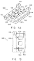
- Fig. 1A shows the internal structure of a conventional semiconductor module.
- a MOSFET is used as an example here.
- a semiconductor module 100 includes a plurality of semiconductor chips 101 which are connected to each other in parallel (three semiconductor modules 101a, 101b and 101c in Fig. 1A).
- a plurality of semiconductor chips 101 are arranged in a straight line with the respective drain region connected to the conductive base substrate 102.
- Semiconductors with such a structure are often termed "non-insulated".
- a source electrode 103 and a gate electrode 104 are formed in parallel with the arranging direction of the plurality of semiconductor chips 101.
- the source electrode 103 and gate electrode 104 are connected to a source region and a gate region, respectively, of each semiconductor chip 101 using bonding wires 105.
- the source electrode 103 and gate electrode 104 are electrically insulated from the base substrate 102 using an insulation sheet 106.
- a drain terminal 107, a source terminal 108 and a gate terminal 109 are connected to the base substrate 102, source electrode 103 and gate electrode 104, respectively.
- the drain terminal 107 and source terminal 108 are an input point and an output point of the main current of this semiconductor module, respectively.
- Each of the semiconductor chips 101 are turned on, when a control voltage is applied between the gate and source.
- the main current which is supplied through the drain terminal 103 reaches the source terminal 108 through the base substrate 102, each of the semiconductor chips 101, bonding wires 105 and source electrode 103 in this order.
- the base substrate 102 functions as a drain electrode.
- a path Ic through the semiconductor chip 101c is substantially longer than a path Ia through the semiconductor chip 101a.
- inductance in a current path is nearly proportional to the length of the path.
- the inductance of the path Ic becomes larger than the inductance of the path Ia.
- this inductance occurs at the time the semiconductor chip 101 is switched (especially, at the time the MOSFET is turned off). Specifically, the larger the inductance, the larger the surge voltage that is generated at the time the semiconductor chip 101 is turned off. Sometimes the semiconductor chip 101 is damaged since this surge voltage is applied to the semiconductor chip 102.
- An object of the present invention is to suppress the surge voltage of a semiconductor module including a plurality of semiconductor elements.
- a semiconductor module of the present invention a plurality of semiconductor chips are arranged in a straight line on a conductive substrate which functions as an electrode for inputting the main current.
- This semiconductor module comprises a terminal for inputting the main current, which is connected to the conductive substrate and is formed in parallel with the arranging direction of the plurality of semiconductor chips, and a terminal which is connected to the respective region for outputting the main current of the plurality of semiconductor chips and is formed in parallel with the arranging direction of the plurality of semiconductor chips.
- the end portion of at least one of the terminal for inputting the main current and terminal for outputting the main current is divided in parallel in the flowing direction of the main current.
- the terminal for inputting the main current is divided into two or more parts, the main current supplied to the respective semiconductor chip is to be inputted through the nearest divided part. If the terminal for outputting the main current is divided into two or more parts, the main current which flows through the respective semiconductor chip is to be outputted to the nearest divided part.
- the terminal for inputting the main current and terminal for outputting the main current are formed in parallel with the arranging direction of the plurality of semiconductor chips, respectively. Therefore, the main current of the respective semiconductor chip flows through the shortest path, and the lengths of all the paths are almost the same each other. As a result, the wiring inductances of all the semiconductor chips become uniform and small, and thus the surge voltages which are applied to the semiconductor chips also become uniform and small.
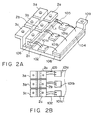
- Figs. 2A and 2B show the internal structure of a semiconductor module, which is one preferred embodiment of the present invention.
- Fig. 2A is the oblique section view
- Fig.2B is the top view.
- a plurality of semiconductor chips 101 (101a through 101c), base substrate 102, gate electrode 104, bonding wire 105, insulation sheet 106 and gate terminal 109 are basically the same as the components used for the conventional semiconductor module shown in Fig. 1A.
- the semiconductor module in this preferred embodiment is characterized mainly in the structure and arrangement of a source electrode, source terminal and drain terminal.
- a source electrode 1 is formed in parallel with the arranging direction of the plurality of semiconductor chips 101, and is connected to the source region of the respective semiconductor chip 101 using bonding wires 105.
- the source electrode 1 is electrically insulated from the base substrate 102 using the insulation sheet 106.
- Source terminals 2a, 2b and 2c are directly connected to the source electrode 1.
- a hole formed in each of the source terminals 2a through 2c is used for connection to an external circuit (including a power supply circuit), etc.
- each of the source terminals 2a through 2c is the output point of the main current in the semiconductor module.
- the widths of all the source terminals 2a through 2c are the same, and are formed in such a way that the width becomes as large as possible.
- the source electrode 1 and source terminals 2a through 2c can be formed monolithically.
- Drain terminals 3a, 3b and 3c are directly connected to the base substrate 102.
- a hole formed in each of the drain terminals 3a through 3c is used for connection to an external circuit (including a power supply circuit), etc.
- each of the drain terminals 3a through 3c is the input point of the main current in the semiconductor module.
- the widths of all the drain terminals 3a through 3c are the same, and are formed in such a way that the width is as large as possible.
- each of the semiconductor chips 101 is turned on, if a control voltage is applied between the gate and source.
- the main current which is supplied through the drain terminals 3a, 3b and 3c reaches the source terminals 2a, 2b and 2c, through the base substrate 102, respective semiconductor chip 101, bonding wires 105 and source electrode 1 in this order.
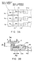
- Figs. 3A and 3B explain the path of the main current in this preferred embodiment.
- a "source terminal 2" indicates an arbitrary source terminal of the source terminals 2a through 2c
- a "drain terminal 3" indicates an arbitrary drain terminal of the drain terminals 3a through 3c.
- the semiconductor module in this preferred embodiment comprises a plurality of drain terminals 3a through 3c and a plurality of source terminals 2a through 2c.
- the semiconductor module in this preferred embodiment has a plurality of main current input points (main current supply points) and a plurality of main current output points.
- the main currents of a plurality of semiconductor chips 101a through 101c are supplied from a plurality of main current input points and are outputted to a plurality of main current output points.
- the main current of the respective semiconductor chip 101a through 101c takes the shortest path of a plurality of paths from a main current input point to a main current output point.
- the main current of the semiconductor chip 101a is supplied from the drain terminal 3a and is outputted to the source terminal 2a.
- the main current of the semiconductor chip 101b is supplied from the drain terminal 3b and is outputted to the source terminal 2b.
- a conventional semiconductor module as shown in Fig. 1B, the paths of some semiconductor chips become long, and the inductances of the paths become large.
- the semiconductor of the preferred embodiment as shown in Fig. 3A, all the paths of the main current of semiconductor chips 101a through 101c have the shortest length. Therefore, the inductance of the respective semiconductor chip becomes small, and the surge voltage applied to the respective semiconductor chip becomes small.
- the semiconductor module in this preferred embodiment can be used in a higher input voltage range even if the conventional semiconductor chips are used.
- the source terminal 2 and drain terminal 3 are closely formed.
- the source terminal 2 and drain terminal 3 are insulated, for example, using a case to protect semiconductor chips 101a through 101c.
- the thickness of the case shall be sufficiently thin such that the source terminal 2 and the drain terminal 3 are close to each other.
- This case is formed of a material which allows magnetic flux to pass.
- the directions of the main current flowing through the source terminal 2 and drain terminal 3 are opposite to each other. For this reason, in a region A1, a magnetic field generated by the main current flowing through the source terminal 2 and a magnetic field generated by the main current flowing through the drain terminal 3 are offset by each other, and thus the inductance of this path becomes reasonably small. In the same way, in a region A2, a magnetic field generated by the main current flowing through the source electrode 1 and a magnetic field generated by main current flowing through the base substrate 102 are offset by each other, and thus the inductance of this path also becomes reasonably small.
- the semiconductor module in this preferred embodiment can be used in a higher input voltage range even if the conventional semiconductor chips are used.
- the source electrode 1 and the source terminals 2a through 2c can be monolithically formed from a piece of a metal plate.
- the source terminals 2a through 2c are formed by bending. The bending is easy and a distortion is small because the portions to be bent (the source terminals 2a through 2c) are divided each other.
- one set of a source terminal and drain terminal are formed for each of the semiconductor chips, the present invention is not limited to this structure.
- one source terminal and one drain terminal can be formed for a plurality of semiconductor chips.
- a source terminal and drain terminal both are divided into two or more parts
- the present invention is not limited to this structure.
- a structure in which a drain terminal is not divided is acceptable.
- a structure in which the source terminal is not divided is acceptable.
- a source electrode can be divided into two or more parts.
- each divided source electrode is connected to one or more source regions of semiconductor chips through bonding wires.
- a semiconductor is assumed to be a MOSFET
- the structure of the present invention can be selected irrespective of the kind of semiconductor device.
- IGBT, GTO, bipolar transistor, thyristor, etc. can be used.
- the wiring inductance of all the semiconductor devices become uniform and small, and thus all the surge voltages become small.
- the upper limit of an input voltage which can be applied to a semiconductor module is extended. If the surge voltage becomes small, a protection circuit, such as a snubber circuit, etc., is not required or the scale of such a protection circuit can be reduced. Accordingly, a semiconductor module itself can be miniaturized.
- a plurality of semiconductor chips are provided on a base substrate.
- a drain region of the respective semiconductor chip is directly connected to the base substrate.
- a source electrode is formed in parallel with the arranging direction of the plurality of semiconductor chips.
- a source electrode and a source region of the respective semiconductor chip are connected using bonding wires.
- a plurality of source terminals are connected to the source electrode.
- a plurality of drain terminals are connected to the base substrate. The source terminal and drain terminal are located close to one another.
Landscapes
- Inverter Devices (AREA)
- Power Conversion In General (AREA)
- Junction Field-Effect Transistors (AREA)
- Insulated Gate Type Field-Effect Transistor (AREA)
- Wire Bonding (AREA)
Abstract
Description
Claims (13)
- A semiconductor module in which a plurality of semiconductor chips (101a, 101b, 101c) are arranged in a straight line on a conductive substrate (102) which functions as an electrode for inputting main current, comprising:a main current input terminal (3a, 3b, 3c), which is connected to the conductive substrate and formed in parallel with an arranging direction of the plurality of semiconductor chips; anda main current output terminal (2a, 2b, 2c), which is connected to each of a plurality of main current output regions of the plurality of semiconductor chips and formed in parallel with the arranging direction of the plurality of semiconductor chips, whereinan end portion of at least one of the main current input terminal and the main current output terminal is divided in parallel in a main current direction.
- The semiconductor module according to claim 1, wherein lengths of said main current input terminal and said main current output terminal are the same as a overall length of a configuration of the plurality of semiconductor chips arranged on the conductive substrate.
- The semiconductor module according to claim 1, wherein if the end portion of said main current input terminal is divided, each divided part is connected to a respective external circuit.
- The semiconductor module according to claim 1, wherein if the end portion of said main current output terminal is divided, each divided part is connected to a respective external circuit.
- The semiconductor module according to claim 1, wherein said main current input terminal and said main current output are located close to one another.
- A semiconductor module including a plurality of semiconductor chips (101a, 101b, 101c), comprising:a first electrode (102) connected to each of main current input regions of the plurality of semiconductor chips; anda second electrode (1) connected to each of main current output regions of the plurality of semiconductor chips, whereinat least one of the first and second electrodes is connected to an external circuit through a plurality of connection points.
- The semiconductor module according to claim 6, wherein said first electrode is a conductive substrate on which the plurality of semiconductor chips are arranged and said second electrode is formed in parallel with an arranging direction of the plurality of semiconductor chips.
- The semiconductor module according to claim 7, further comprisinga first terminal (11 or 3a, 3b, 3c) connected to said first electrode, whereinsaid first terminal is formed in parallel with the arranging direction of the plurality of semiconductor chips, with the length of said first terminal being the same as length of overall configuration of the plurality of semiconductor chips, and said first electrode is connected to the external circuit through said first terminal.
- The semiconductor module according to claim 8, wherein an end portion of said first terminal is divided into two or more parts, and each divided part is connected to the respective external circuit.
- The semiconductor module according to claim 7, further comprisinga plurality of first terminals (3a, 3b, 3c) connected to said first electrode, whereinsaid first electrode is connected to the external circuit through the plurality of first terminals.
- The semiconductor module according to claim 7, wherein the length of said second electrode is the same as the length of overall configuration of the plurality of semiconductor chips, and said second electrode is connected to the external circuit through a plurality of connection points.
- The semiconductor module according to claim 11, wherein a plurality of terminals (2a, 2b, 2c) are formed in an end portion of said second electrode, and each terminal is connected to the respective external circuit.
- The semiconductor module according to claim 11, further comprisinga plurality of second terminals (2a, 2b, 2c) connected to said second electrode, whereinsaid second electrode is connected to the external circuit through the plurality of second terminals.
Applications Claiming Priority (2)
| Application Number | Priority Date | Filing Date | Title |
|---|---|---|---|
| JP25361298A JP3521757B2 (en) | 1998-09-08 | 1998-09-08 | Semiconductor module electrode structure |
| JP25361298 | 1998-09-08 |
Publications (3)
| Publication Number | Publication Date |
|---|---|
| EP0987762A2 true EP0987762A2 (en) | 2000-03-22 |
| EP0987762A3 EP0987762A3 (en) | 2000-11-08 |
| EP0987762B1 EP0987762B1 (en) | 2003-05-07 |
Family
ID=17253799
Family Applications (1)
| Application Number | Title | Priority Date | Filing Date |
|---|---|---|---|
| EP99117597A Expired - Lifetime EP0987762B1 (en) | 1998-09-08 | 1999-09-07 | Semiconductor module |
Country Status (5)
| Country | Link |
|---|---|
| US (1) | US6566750B1 (en) |
| EP (1) | EP0987762B1 (en) |
| JP (1) | JP3521757B2 (en) |
| DE (1) | DE69907590T2 (en) |
| TW (1) | TW437083B (en) |
Cited By (6)
| Publication number | Priority date | Publication date | Assignee | Title |
|---|---|---|---|---|
| EP1150429A1 (en) * | 2000-04-28 | 2001-10-31 | Denso Corporation | Load drive circuit having parallel-connected switch circuits |
| WO2002058150A1 (en) * | 2001-01-19 | 2002-07-25 | Siemens Aktiengesellschaft | Circuit arrangement with semiconductor elements arranged in chips |
| WO2002082543A1 (en) * | 2001-03-30 | 2002-10-17 | Hitachi, Ltd. | Semiconductor device |
| FR2828580A1 (en) * | 2001-08-08 | 2003-02-14 | Mitsubishi Electric Corp | POWER MODULE |
| WO2004107442A1 (en) * | 2003-05-27 | 2004-12-09 | Siemens Aktiengesellschaft | Bi-directional switch, and use of said switch |
| EP1315206A3 (en) * | 2001-11-26 | 2006-03-29 | Kabushiki Kaisha Toyota Jidoshokki | Semiconductor apparatus of a plurality of semiconductor devices enclosed in a case and wiring method therefore |
Families Citing this family (12)
| Publication number | Priority date | Publication date | Assignee | Title |
|---|---|---|---|---|
| DE10237561C1 (en) * | 2002-08-16 | 2003-10-16 | Semikron Elektronik Gmbh | Power semiconductor circuit device has DC and AC terminal leads extending parallel to substrate and/or connector paths and provided with surface elements for bonding wire connections |
| US6982482B2 (en) * | 2004-02-24 | 2006-01-03 | Applied Pulsed Power, Inc. | Packaging of solid state devices |
| JP4513770B2 (en) * | 2006-02-28 | 2010-07-28 | 株式会社豊田自動織機 | Semiconductor device |
| DE102006034599B4 (en) * | 2006-07-26 | 2010-01-21 | Infineon Technologies Ag | Method for interconnecting semiconductor chips produced from a wafer |
| US7781872B2 (en) * | 2007-12-19 | 2010-08-24 | Fairchild Semiconductor Corporation | Package with multiple dies |
| US7626249B2 (en) * | 2008-01-10 | 2009-12-01 | Fairchild Semiconductor Corporation | Flex clip connector for semiconductor device |
| JP5136343B2 (en) * | 2008-10-02 | 2013-02-06 | 三菱電機株式会社 | Semiconductor device |
| US9147666B2 (en) | 2009-05-14 | 2015-09-29 | Rohm Co., Ltd. | Semiconductor device |
| WO2014091608A1 (en) * | 2012-12-13 | 2014-06-19 | 株式会社 日立製作所 | Power semiconductor module and power conversion apparatus using same |
| JP6252194B2 (en) * | 2014-01-17 | 2017-12-27 | 株式会社豊田自動織機 | Semiconductor device |
| CN109511278B (en) * | 2017-07-14 | 2022-06-17 | 新电元工业株式会社 | Electronic module |
| CN111540730B (en) * | 2020-04-22 | 2021-08-13 | 西安交通大学 | Packaging structure of multi-chip wide bandgap power module based on conductive metal clip interconnection |
Family Cites Families (5)
| Publication number | Priority date | Publication date | Assignee | Title |
|---|---|---|---|---|
| JPS61139051A (en) | 1984-12-11 | 1986-06-26 | Toshiba Corp | Semiconductor device |
| US5233235A (en) * | 1988-08-16 | 1993-08-03 | Siemens Aktiengesellschaft | On-chip intermediate driver for discrete WSI systems |
| JP3053298B2 (en) | 1992-08-19 | 2000-06-19 | 株式会社東芝 | Semiconductor device |
| JP3186925B2 (en) * | 1994-08-04 | 2001-07-11 | シャープ株式会社 | Panel mounting structure, integrated circuit mounting tape and method of manufacturing the same |
| JP3267169B2 (en) | 1996-09-06 | 2002-03-18 | 株式会社日立製作所 | Power semiconductor device |
-
1998
- 1998-09-08 JP JP25361298A patent/JP3521757B2/en not_active Expired - Lifetime
-
1999
- 1999-09-03 US US09/389,327 patent/US6566750B1/en not_active Expired - Lifetime
- 1999-09-07 TW TW088115393A patent/TW437083B/en not_active IP Right Cessation
- 1999-09-07 DE DE69907590T patent/DE69907590T2/en not_active Expired - Lifetime
- 1999-09-07 EP EP99117597A patent/EP0987762B1/en not_active Expired - Lifetime
Cited By (10)
| Publication number | Priority date | Publication date | Assignee | Title |
|---|---|---|---|---|
| EP1150429A1 (en) * | 2000-04-28 | 2001-10-31 | Denso Corporation | Load drive circuit having parallel-connected switch circuits |
| US6417652B1 (en) | 2000-04-28 | 2002-07-09 | Denso Corporation | Load drive circuit for an electric load |
| WO2002058150A1 (en) * | 2001-01-19 | 2002-07-25 | Siemens Aktiengesellschaft | Circuit arrangement with semiconductor elements arranged in chips |
| US6940136B2 (en) | 2001-01-19 | 2005-09-06 | Siemens Aktiengesellschaft | Circuit arrangement with semiconductor elements arranged in chips |
| WO2002082543A1 (en) * | 2001-03-30 | 2002-10-17 | Hitachi, Ltd. | Semiconductor device |
| US6943445B2 (en) | 2001-03-30 | 2005-09-13 | Hitachi, Ltd. | Semiconductor device having bridge-connected wiring structure |
| FR2828580A1 (en) * | 2001-08-08 | 2003-02-14 | Mitsubishi Electric Corp | POWER MODULE |
| EP1315206A3 (en) * | 2001-11-26 | 2006-03-29 | Kabushiki Kaisha Toyota Jidoshokki | Semiconductor apparatus of a plurality of semiconductor devices enclosed in a case and wiring method therefore |
| US7161235B2 (en) | 2001-11-26 | 2007-01-09 | Kabushiki Kaisha Toyota Jidoshokki | Semiconductor apparatus of a plurality of semiconductor devices enclosed in case and wiring method therefore |
| WO2004107442A1 (en) * | 2003-05-27 | 2004-12-09 | Siemens Aktiengesellschaft | Bi-directional switch, and use of said switch |
Also Published As
| Publication number | Publication date |
|---|---|
| DE69907590D1 (en) | 2003-06-12 |
| JP2000091498A (en) | 2000-03-31 |
| US6566750B1 (en) | 2003-05-20 |
| DE69907590T2 (en) | 2004-04-01 |
| EP0987762A3 (en) | 2000-11-08 |
| TW437083B (en) | 2001-05-28 |
| JP3521757B2 (en) | 2004-04-19 |
| EP0987762B1 (en) | 2003-05-07 |
Similar Documents
| Publication | Publication Date | Title |
|---|---|---|
| US6566750B1 (en) | Semiconductor module | |
| US8466561B2 (en) | Semiconductor module with a power semiconductor chip and a passive component and method for producing the same | |
| CN102067309B (en) | Power semiconductor module | |
| US10319671B2 (en) | Semiconductor package with leadframe | |
| US7095099B2 (en) | Low profile package having multiple die | |
| US20070108575A1 (en) | Semiconductor package that includes stacked semiconductor die | |
| KR20150140600A (en) | Power semiconductor device | |
| US20220254700A1 (en) | Packaged power semiconductor device | |
| US12489103B2 (en) | Semiconductor module | |
| US10699987B2 (en) | SMD package with flat contacts to prevent bottleneck | |
| CN110364499B (en) | Multi-Package Top-Side Cooling | |
| US11329000B2 (en) | Package for a multi-chip power semiconductor device | |
| US6521992B2 (en) | Semiconductor apparatus | |
| US12412815B2 (en) | Semiconductor package and method of manufacturing a semiconductor package | |
| US6664629B2 (en) | Semiconductor device | |
| CN112447612B (en) | Multi-chip package | |
| US6232654B1 (en) | Semiconductor module | |
| JPH11177021A (en) | Electrode structure of semiconductor switch | |
| US20230146272A1 (en) | Semiconductor apparatus | |
| US20250118634A1 (en) | Intelligent power module arrangement | |
| US20250022835A1 (en) | Semiconductor module | |
| US12500185B2 (en) | Semiconductor device | |
| US20230268255A1 (en) | Power Semiconductor Device | |
| US20240088796A1 (en) | Semiconductor module | |
| US20240297148A1 (en) | Power module with improved semiconductor die arrangement for active clamping |
Legal Events
| Date | Code | Title | Description |
|---|---|---|---|
| PUAI | Public reference made under article 153(3) epc to a published international application that has entered the european phase |
Free format text: ORIGINAL CODE: 0009012 |
|
| 17P | Request for examination filed |
Effective date: 19990907 |
|
| AK | Designated contracting states |
Kind code of ref document: A2 Designated state(s): DE FR GB SE |
|
| AX | Request for extension of the european patent |
Free format text: AL;LT;LV;MK;RO;SI |
|
| PUAL | Search report despatched |
Free format text: ORIGINAL CODE: 0009013 |
|
| AK | Designated contracting states |
Kind code of ref document: A3 Designated state(s): AT BE CH CY DE DK ES FI FR GB GR IE IT LI LU MC NL PT SE |
|
| AX | Request for extension of the european patent |
Free format text: AL;LT;LV;MK;RO;SI |
|
| RIC1 | Information provided on ipc code assigned before grant |
Free format text: 7H 01L 25/065 A, 7H 01L 25/07 B |
|
| AKX | Designation fees paid |
Free format text: DE FR GB SE |
|
| 17Q | First examination report despatched |
Effective date: 20011001 |
|
| RAP1 | Party data changed (applicant data changed or rights of an application transferred) |
Owner name: KABUSHIKI KAISHA TOYOTA JIDOSHOKKI |
|
| GRAH | Despatch of communication of intention to grant a patent |
Free format text: ORIGINAL CODE: EPIDOS IGRA |
|
| GRAH | Despatch of communication of intention to grant a patent |
Free format text: ORIGINAL CODE: EPIDOS IGRA |
|
| GRAA | (expected) grant |
Free format text: ORIGINAL CODE: 0009210 |
|
| AK | Designated contracting states |
Designated state(s): DE FR GB SE |
|
| REG | Reference to a national code |
Ref country code: GB Ref legal event code: FG4D |
|
| REF | Corresponds to: |
Ref document number: 69907590 Country of ref document: DE Date of ref document: 20030612 Kind code of ref document: P |
|
| REG | Reference to a national code |
Ref country code: SE Ref legal event code: TRGR |
|
| ET | Fr: translation filed | ||
| PLBE | No opposition filed within time limit |
Free format text: ORIGINAL CODE: 0009261 |
|
| STAA | Information on the status of an ep patent application or granted ep patent |
Free format text: STATUS: NO OPPOSITION FILED WITHIN TIME LIMIT |
|
| 26N | No opposition filed |
Effective date: 20040210 |
|
| REG | Reference to a national code |
Ref country code: FR Ref legal event code: PLFP Year of fee payment: 18 |
|
| REG | Reference to a national code |
Ref country code: FR Ref legal event code: PLFP Year of fee payment: 19 |
|
| REG | Reference to a national code |
Ref country code: FR Ref legal event code: PLFP Year of fee payment: 20 |
|
| PGFP | Annual fee paid to national office [announced via postgrant information from national office to epo] |
Ref country code: FR Payment date: 20180813 Year of fee payment: 20 Ref country code: DE Payment date: 20180828 Year of fee payment: 20 |
|
| PGFP | Annual fee paid to national office [announced via postgrant information from national office to epo] |
Ref country code: GB Payment date: 20180905 Year of fee payment: 20 Ref country code: SE Payment date: 20180910 Year of fee payment: 20 |
|
| REG | Reference to a national code |
Ref country code: DE Ref legal event code: R071 Ref document number: 69907590 Country of ref document: DE |
|
| REG | Reference to a national code |
Ref country code: GB Ref legal event code: PE20 Expiry date: 20190906 |
|
| REG | Reference to a national code |
Ref country code: SE Ref legal event code: EUG |
|
| PG25 | Lapsed in a contracting state [announced via postgrant information from national office to epo] |
Ref country code: GB Free format text: LAPSE BECAUSE OF EXPIRATION OF PROTECTION Effective date: 20190906 |