EP0986166B1 - Charge pump circuit - Google Patents
Charge pump circuit Download PDFInfo
- Publication number
- EP0986166B1 EP0986166B1 EP19990117576 EP99117576A EP0986166B1 EP 0986166 B1 EP0986166 B1 EP 0986166B1 EP 19990117576 EP19990117576 EP 19990117576 EP 99117576 A EP99117576 A EP 99117576A EP 0986166 B1 EP0986166 B1 EP 0986166B1
- Authority
- EP
- European Patent Office
- Prior art keywords
- transistor
- charge pump
- terminal
- pump circuit
- input
- Prior art date
- Legal status (The legal status is an assumption and is not a legal conclusion. Google has not performed a legal analysis and makes no representation as to the accuracy of the status listed.)
- Expired - Lifetime
Links
Images


Classifications
-
- H—ELECTRICITY
- H02—GENERATION; CONVERSION OR DISTRIBUTION OF ELECTRIC POWER
- H02M—APPARATUS FOR CONVERSION BETWEEN AC AND AC, BETWEEN AC AND DC, OR BETWEEN DC AND DC, AND FOR USE WITH MAINS OR SIMILAR POWER SUPPLY SYSTEMS; CONVERSION OF DC OR AC INPUT POWER INTO SURGE OUTPUT POWER; CONTROL OR REGULATION THEREOF
- H02M3/00—Conversion of dc power input into dc power output
- H02M3/02—Conversion of dc power input into dc power output without intermediate conversion into ac
- H02M3/04—Conversion of dc power input into dc power output without intermediate conversion into ac by static converters
- H02M3/06—Conversion of dc power input into dc power output without intermediate conversion into ac by static converters using resistors or capacitors, e.g. potential divider
- H02M3/07—Conversion of dc power input into dc power output without intermediate conversion into ac by static converters using resistors or capacitors, e.g. potential divider using capacitors charged and discharged alternately by semiconductor devices with control electrode, e.g. charge pumps
- H02M3/073—Charge pumps of the Schenkel-type
Definitions
- charge pump circuits or charge pumps are the supply of a connected to the output terminal, preferably capacitive load, with an output voltage whose value exceeds the value of an available supply voltage which can be applied to the input terminal.
- Such circuits are in EP-A-0403823 discloses and finds use, for example, in memory modules, such as EEPROMs, in which high voltages are briefly required for writing the memory cells.
- charge pump circuits are used for driving power MOSFET, which serve to drive a source side connected load.
- a number of the known charge pumps are usually cascaded to a multistage charge pump.
- the output terminal is connected in each case a charge pump to the input terminal of a subsequent charge pump.
- the provision of the output voltage at the output terminal of each charge pump, or the charging of a capacitive load connected there, requires a multi-stage process, in which the first capacity is charged via the input terminal in a first step.
- the first transistor conducts and a capacitor connected downstream of the output terminal can be charged to a voltage substantially above the magnitude of the first drive potential above the voltage the first capacity is located.
- the control electrode of the first transistor is connected by the second capacitance and the second drive potential at a potential which exceeds the potential at the input terminal and thus ensures a safe conduction of the first transistor and thus minimizing the voltage losses across the load path.
- the purpose of the second transistor is to short-circuit the control electrode of the first transistor with its load terminal connected to the input terminal after the first drive potential has been withdrawn, in order to block the first transistor and thereby prevent a backflow of the charge delivered to the output terminal.
- the control electrode of the second transistor connected to the first capacitor of a subsequent charge pump stage, it being ensured that due to the higher potential applied thereto after the pumping operation has ended, the second transistor conducts the blocking of the first transistor.
- the disadvantage of such a coupling of the second transistor to the next higher pumping stage is that for the last pumping stage, at the output terminal of the load is connected, no second transistor for blocking the first transistor and thus no second capacitance can be provided.
- the control electrode of the first transistor of this last pump stage is above the first diode at the maximum at the potential of the load terminal connected to the input terminal. This results in voltage losses over the load path of the first transistor of this last pump stage, which worsen the efficiency of the overall arrangement of a plurality of charge pumps.
- the object of the present invention is to provide a charge pump circuit in which, independently of a further connection, voltage losses across the load path of the first transistor acting as a switch are minimized.
- a charge pump circuit mentioned in the opening paragraph which additionally has a charge storage circuit having a first terminal connected to the control electrode of the first transistor and a second terminal connected to the control electrode of the second transistor.
- the charge storage circuit takes on concern of the second drive potential at the second control terminal on a charge on its first terminal.
- the circuit arrangement is dimensioned such that the potential caused at the second terminal by this charge is less than or equal to the potential at the input terminal and thus at the load path terminal of the second transistor as long as the first drive potential applied to the first control terminal; the second transistor then largely blocks.
- the potential at the control electrode of the second transistor exceeds the potential at the input terminal; the second transistor conducts and short circuits the control electrode of the first transistor with its load terminal connected to the input terminal.
- the first transistor blocks and prevents backflow of charge to the first capacitor.
- the charge storage circuit comprises a series connection of a diode and a capacitor, one terminal of the diode being connected to the control electrode of the first transistor and one of the diode and the common node capacitance being connected to the control electrode of the second transistor is.
- This embodiment represents a simple realization of the charge storage circuit in which the charge to be stored can flow through the diode to the capacitor, the diode preventing the charge from flowing back.
- the electrode facing away from the common node of the capacitance is connected to a constant supply potential. This supply potential causes a bias of the common node to which the control electrode of the second transistor is connected, whereby less charge must be absorbed via the diode.
- the invention further provides a method according to claim 8.
- the invention will be described below using field effect transistors (FET) for the transistors occurring in the charge pump circuit according to the invention.
- FET field effect transistors
- the control electrode corresponds to the gate electrode, the load path of the drain-source path or the load path terminals to the drain and source terminals.
- Fig. 1 shows a charge pump circuit according to the invention with an input terminal EK, an output terminal AK, a first control input SK1 and a second control input SK2.
- the output terminal is connected downstream of a capacitive load L by way of example.
- the capacitive load L shown as a capacitor represents all types of capacitive loads, including write lines of EEPROMs, gate electrodes of MOSFETs or other charge pump circuits according to the invention.
- the first transistor T1 is connected, whose gate electrode G is connected via a first diode D1 to the input terminal EK.
- a first capacitor C1 Between the first control input SK1 and the input terminal EK is a first capacitor C1, between the second control input SK2 and the gate electrode G of the first transistor T1, a second capacitor C2 is connected.
- the task of the first transistor T1 is to establish an electrically conductive connection between the input terminal EK and the output terminal AK in order to allow a charge stored on the first capacitor C1 to flow to the capacitive load L.
- a second transistor T2 In order to block the first transistor T1 and thus prevent the charge from flowing back from the capacitive load L, a second transistor T2, likewise designed as an n-channel MOSFET, is provided between the gate electrode G of the first transistor T1 and the input terminal EK is switched.
- a circuit LS is provided for charge storage, which is connected to a first terminal K1 to the gate electrode G of the first transistor T1 and a second terminal K2 to the gate electrode G of the second transistor T2.
- the circuit LS has a series arrangement of a diode D2 and a capacitor C3, the diode D2 having a terminal to the first terminal K1 of the circuit arrangement LS is connected and wherein one of the diode D2 and the capacitor C3 common node N is connected to the second terminal K2 of the circuit LS and thus to the gate electrode G of the second transistor T2.
- a terminal of the capacitance C3 facing away from the common node N is connected to a supply potential Vc.
- the object of the charge pump circuit according to the invention is to provide an output voltage for the load L connected to the output terminal AK or to charge the capacitive load to a voltage which is above the value of a voltage supplied to the input terminal EK.
- the charging of the capacitive load L is carried out in a multi-stage process, wherein in a first step, the first capacitor C1 is charged via a connectable to the input terminal EK charge source, the input terminal is disconnected after charging the first capacitor C1 from the charge source.
- a charge source for example, a constant voltage source is considered, which is switched to the input source for a predetermined period of time.
- the charge source is again a charge pump circuit according to the invention, whose output terminal is connected to the input terminal of the illustrated charge pump circuit.
- One of the input terminals EK advantageously upstream diode D3 prevents leakage of the charge stored in the first capacitor C1 via the input terminal EK. In the case of multistage charge pumps, such a diode is required only in front of the input terminal of the first pumping stage.
- the input terminal EK is at a first potential.
- a first drive potential V1 at the first Control input SK1 which until then was preferably at a reference potential M, increases by a value V +, the potential at the input terminal also increases accordingly.
- Both the gate electrode G of the first transistor T1 and the second capacitor C2 are charged via the first diode D1, wherein the value of the potential which occurs there is reduced by the value of the voltage drop across the first diode D1.
- the first diode as in Fig. 2 represented a self-conducting field effect transistor T3 used, which is connected as a diode. The advantage is that the voltage dropping across the diode-connected field effect transistor T3 in the flux direction is almost zero.
- the second capacitance C2 is advantageously dimensioned substantially smaller than the first capacitance C1 in order to be able to deliver the charge stored on the first capacitance C1 as completely as possible to the load L. If the gate electrode G of the first transistor T1 is charged to the potential at the input terminal EK, and this potential exceeds the potential applied to the source electrode S of the first transistor T1 or to the output terminal AK, the first transistor T1 starts to conduct. The charge stored on the first capacitor C1 flows through the output terminal AK to the load L. In this case, the potential at the output terminal AK or at the source electrode S of the first transistor T1 increases, whereby its conductivity is reduced.
- the potential at the gate electrode G of the first transistor T1 thus also increases.
- the gate potential of the first transistor T1 is thus ideally around the value V + above the potential applied to the input terminal EK and thereby maximally applied to the output terminal AK.
- the capacitive load in view of only small losses across the load path DS of the first transistor T1, can be approximately charged to the potential applied to the input terminal, which is about the value V + above the potential originally provided at the input terminal EK.
- the load may only flow into the charge stored on the first capacitor so that, depending on the capacity ratio of the first capacitor C1 to the load L, the described method may need to be repeated several times to charge the load to the higher voltage.
- the capacitance C3 of the circuit arrangement LS for charge storage is also charged via the diode D2.
- the node N common to the diode D2 and the capacitance C3 is biased by the supply voltage source Vc, whereby a smaller charge flows to the capacitor C3 than would be required in the case of a connection of the capacitance to the reference potential M.
- the diode D2, which may also be formed as a transistor T4, as in Fig. 2 is shown, is dimensioned so that the potential applied to the common node N potential does not exceed the value of the potential at the input terminal EK, as long as applied to the first control input to the V + increased driving potential V1. This ensures that during the pumping operation, ie, while "charge" is being pumped from the first capacitor C1 to the load L, the second transistor T2 does not conduct and thus does not block the first transistor T1.
- the second drive potential V2 and the first drive potential V1 are withdrawn, preferably one after the other, and the first and second control inputs SK1, SK2 are preferably connected to reference potential M.
- the voltage applied to the gate electrode G of the second transistor T2 then exceeds the voltage applied to the input terminal EK Potential or the voltage applied across the discharged first capacitor C1 voltage.
- the second transistor T2 conducts and discharges the gate electrode G of the first transistor T1, which thereby blocks and prevents backflow of the charge from the load L to the first capacitor C1.
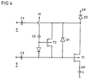
- Fig. 3 shows the charge pump circuit according to the invention when using p-channel MOSFET for the first and second transistors.
- the sign of the voltages occurring at the individual components and also the drive voltages V1, V2 (see Fig. 5 ) is opposite to that in the Ladugnspumpenscen according to Fig. 1 and 2 occurring voltages vice versa.
- the polarity of the diodes D1, D2 is reversed in this embodiment.
Description
Die vorliegende Erfindung betrifft eine Ladungspumpenschaltung die folgende Merkmale aufweist:
- eine Eingangsklemme, eine Ausgangsklemme, einen ersten Steuereingang und einen zweiten Steuereingang;
- einen ersten Transistor mit einer Laststrecke, die zwischen die Eingangsklemme und die Ausgangsklemme geschaltet ist, und mit einer Steuerelektrode, die über eine erste Diode an die Eingangsklemme angeschlossen ist;
- eine erste Kapazität, die zwischen den ersten Steuereingang und die Eingangsklemme geschaltet ist;
- eine zweite Kapazität, die zwischen den zweiten Steuereingang und die Steuerelektrode des ersten Transistors geschaltet ist;
- einen zweiten Transistor mit einer Steuerelektrode und mit einer Laststrecke, die zwischen die Eingangsklemme und die Steuerelektrode des ersten Transistors geschaltet ist.
- an input terminal, an output terminal, a first control input and a second control input;
- a first transistor having a load path connected between the input terminal and the output terminal and having a control electrode connected to the input terminal via a first diode;
- a first capacitance connected between the first control input and the input terminal;
- a second capacitance connected between the second control input and the control electrode of the first transistor;
- a second transistor having a control electrode and a load path connected between the input terminal and the control electrode of the first transistor.
Die Funktion derartiger Ladungspumpenschaltungen oder Ladungspumpen ist die Versorgung einer an die Ausgangsklemme angeschlossenen, vorzugsweise kapazitiven Last, mit einer Ausgangsspannung, deren Wert den Wert einer zur Verfügung stehenden Versorgungsspannung, die an die Eingangsklemme anlegbar ist, übersteigt. Derartige Schaltungen sind in
Zum Erreichen großer Ausgangsspannungen werden üblicherweise eine Anzahl der bekannten Ladungspumpen zu einer mehrstufigen Ladungspumpe kaskadiert. Hierzu wird die Ausgangsklemme jeweils einer Ladungspumpe an die Eingangsklemme einer nachfolgenden Ladungspumpe angeschlossen. Die Ausgangsklemme der letzten Ladungspumpe in der Kaskade, der keine weitere Ladungspumpe nachgeschaltet ist, bildet dabei den Anschluß für die anzusteuernde Last.To achieve high output voltages, a number of the known charge pumps are usually cascaded to a multistage charge pump. For this purpose, the output terminal is connected in each case a charge pump to the input terminal of a subsequent charge pump. The output terminal of the last charge pump in the cascade, which is followed by no further charge pump, thereby forms the connection for the load to be controlled.
Die Bereitstellung der Ausgangsspannung an der Ausgangsklemme jeder einzelnen Ladungspumpe, bzw. das Aufladen einer dort angeschlossenen kapazitiven Last, erfordert ein mehrstufiges Verfahren, bei dem in einem ersten Schritt die erste Kapazität über die Eingangsklemme aufgeladen wird. Durch Anlegen eines ersten Ansteuerpotentials an die erste Steuerklemme und durch nachfolgendes Anlegen eines zweiten Ansteuerpotentials an die zweite Steuerelektrode leitet der erste Transistor und eine der Ausgangsklemme nachgeschaltete Kapazität kann auf eine Spannung aufgeladen werden, die im wesentlichen um den Betrag des ersten Ansteuerpotentials über der Spannung an der ersten Kapazität liegt. Die Steuerelektrode des ersten Transistors liegt durch die zweite Kapazität und das zweite Ansteuerpotentials an einem Potential, welches das Potential an der Eingangsklemme übersteigt und damit ein sicheres Leiten des ersten Transistors und damit eine Minimierung der Spannungsverluste über dessen Laststrecke gewährleistet.The provision of the output voltage at the output terminal of each charge pump, or the charging of a capacitive load connected there, requires a multi-stage process, in which the first capacity is charged via the input terminal in a first step. By applying a first drive potential to the first control terminal and then applying a second drive potential to the second control electrode, the first transistor conducts and a capacitor connected downstream of the output terminal can be charged to a voltage substantially above the magnitude of the first drive potential above the voltage the first capacity is located. The control electrode of the first transistor is connected by the second capacitance and the second drive potential at a potential which exceeds the potential at the input terminal and thus ensures a safe conduction of the first transistor and thus minimizing the voltage losses across the load path.
Aufgabe des zweiten Transistors ist es hierbei, nach Zurücknahme des ersten Ansteuerpotentials die Steuerelektrode des ersten Transistors mit seinem an die Eingangsklemme angeschlossenen Laststreckenanschluß kurzzuschließen, um den ersten Transistor zu sperren und dadurch ein Zurückfließen der an die Ausgangsklemme abgegebenen Ladung zu verhindern. Bei den bekannten Ladungspumpenschaltungen ist die Steuerelektrode des zweiten Transistors an die erste Kapazität einer nachfolgenden Ladungspumpenstufe angeschlossen, wobei aufgrund des nach Abschluß des Pumpvorgangs dort anliegenden höheren Potentials sichergestellt ist, daß der zweite Transistor zum Sperren des ersten Transistors leitet.The purpose of the second transistor is to short-circuit the control electrode of the first transistor with its load terminal connected to the input terminal after the first drive potential has been withdrawn, in order to block the first transistor and thereby prevent a backflow of the charge delivered to the output terminal. In the known charge pump circuits, the control electrode of the second transistor connected to the first capacitor of a subsequent charge pump stage, it being ensured that due to the higher potential applied thereto after the pumping operation has ended, the second transistor conducts the blocking of the first transistor.
Nachteilig einer derartigen Kopplung des zweiten Transistors an die nächsthöhere Pumpstufe ist, daß für die letzte Pumpstufe, an deren Ausgangsklemme die Last angeschlossen ist, kein zweiter Transistor zum Sperren des ersten Transistors und damit auch keine zweite Kapazität vorgesehen werden kann. Die Steuerelektrode des ersten Transistors dieser letzten Pumpstufe liegt über die erste Diode maximal auf dem Potential des mit der Eingangsklemme verbundenen Laststreckenanschlusses. Hierdurch ergeben sich über der Laststrecke des ersten Transistors dieser letzten Pumpstufe Spannungsverluste, die den Wirkungsgrad der Gesamtanordnung aus mehreren Ladungspumpen verschlechtern.The disadvantage of such a coupling of the second transistor to the next higher pumping stage is that for the last pumping stage, at the output terminal of the load is connected, no second transistor for blocking the first transistor and thus no second capacitance can be provided. The control electrode of the first transistor of this last pump stage is above the first diode at the maximum at the potential of the load terminal connected to the input terminal. This results in voltage losses over the load path of the first transistor of this last pump stage, which worsen the efficiency of the overall arrangement of a plurality of charge pumps.
Gleiches gilt, wenn nur eine Ladungspumpe mit einer Pumpstufe benötigt wird.The same applies if only one charge pump with one pump stage is needed.
Aufgabe der vorliegenden Erfindung ist es eine Ladungspumpenschaltung zur Verfügung zu stellen, bei der unabhängig von einer weiteren Verschaltung Spannungsverluste über der Laststrecke des als Schalter wirkenden ersten Transistors minimiert sind.The object of the present invention is to provide a charge pump circuit in which, independently of a further connection, voltage losses across the load path of the first transistor acting as a switch are minimized.
Diese Aufgabe wird durch eine eingangs erwähnte Ladungspumpenschaltung gelöst, die zusätzlich eine Schaltungsanordnung zur Ladungsspeicherung aufweist mit einer ersten Klemme, die an die Steuerelektrode des ersten Transistors angeschlossen ist, und mit einer zweiten Klemme, die an die Steuerelektrode des zweiten Transistors angeschlossen ist.This object is achieved by a charge pump circuit mentioned in the opening paragraph, which additionally has a charge storage circuit having a first terminal connected to the control electrode of the first transistor and a second terminal connected to the control electrode of the second transistor.
Die erfindungsgemäße Schaltungsanordnung zur Ladungsspeicherung nimmt bei Anliegen des zweiten Ansteuerpotentials an der zweiten Steuerklemme eine Ladung über ihre erste Klemme auf. Die Schaltungsanordnung ist dabei so dimensioniert, daß das an der zweiten Klemme durch diese Ladung hervorgerufene Potential kleiner oder gleich dem Potential an der Eingangsklemme -und damit an dem Laststreckenanschluß des zweiten Transistors ist- solange das erste Ansteuerpotential an der ersten Steuerklemme anliegt; der zweite Transistor sperrt dann weitgehend. Nach Zurücknehmen des ersten Ansteuerpotentials übersteigt das Potential an der Steuerelektrode des zweiten Transistors das Potential an der Eingangsklemme; der zweite Transistor leitet und schließt so die Steuerelektrode des ersten Transistors mit seinem an die Eingangsklemme angeschlossenen Laststreckenanschluß kurz. Der erste Transistor sperrt und verhindert ein Zurückfließen von Ladung auf die erste Kapazität.The charge storage circuit according to the invention takes on concern of the second drive potential at the second control terminal on a charge on its first terminal. The circuit arrangement is dimensioned such that the potential caused at the second terminal by this charge is less than or equal to the potential at the input terminal and thus at the load path terminal of the second transistor as long as the first drive potential applied to the first control terminal; the second transistor then largely blocks. Upon withdrawal of the first drive potential, the potential at the control electrode of the second transistor exceeds the potential at the input terminal; the second transistor conducts and short circuits the control electrode of the first transistor with its load terminal connected to the input terminal. The first transistor blocks and prevents backflow of charge to the first capacitor.
Vorteilhafte Ausgestaltungen der Erfindung sind Gegenstand der Unteransprüche.Advantageous embodiments of the invention are the subject of the dependent claims.
Gemäß einer Ausführungsform der Erfindung ist vorgesehen, daß die Schaltungsanordnung zur Ladungsspeicherung eine Reihenschaltung einer Diode und einer Kapazität aufweist, wobei eine Klemme der Diode an die Steuerelektrode des ersten Transistors und wobei ein der Diode und der Kapazität gemeinsamer Knoten an die Steuerelektrode des zweiten Transistors angeschlossen ist. Diese Ausführungsform stellt eine einfache Realisierung der Schaltungsanordnung zur Ladungsspeicherung dar, bei der die zu speichernde Ladung über die Diode auf die Kapazität fließen kann, wobei die Diode ein Zurückfließen der Ladung verhindert. Vorteilhafterweise ist die dem gemeinsamen Knoten abgewandte Elektrode der Kapazität an ein konstantes Versorgungspotential angeschlossen. Dieses Versorgungspotential bewirkt eine Vorspannung des gemeinsamen Knotens, an den die Steuerelektrode des zweiten Transistors angeschlossen ist, wodurch weniger Ladung über die Diode aufgenommen werden muß.According to an embodiment of the invention, it is provided that the charge storage circuit comprises a series connection of a diode and a capacitor, one terminal of the diode being connected to the control electrode of the first transistor and one of the diode and the common node capacitance being connected to the control electrode of the second transistor is. This embodiment represents a simple realization of the charge storage circuit in which the charge to be stored can flow through the diode to the capacitor, the diode preventing the charge from flowing back. Advantageously, the electrode facing away from the common node of the capacitance is connected to a constant supply potential. This supply potential causes a bias of the common node to which the control electrode of the second transistor is connected, whereby less charge must be absorbed via the diode.
Gegenstand der Erfindung ist des weiteren ein Verfahren gemäß Patentanspruch 8.The invention further provides a method according to claim 8.
Vorteilhafte Ausgestaltungen der Erfindung werden nachfolgend in Ausführungsbeispielen anhand von Figuren näher erläutert. Es zeigen:
- Fig. 1
- erfindungsgemäße Ladungspumpenschaltung gemäß einer ersten Ausführungsform;
- Fig. 2
- erfindungsgemäße Ladungspumpenschaltung gemäß einer zweiten Ausführungsform;
- Fig. 3
- erste und zweite Ansteuerpotentiale über der Zeit zur Durchführung des erfindungsgemäßen Verfahrens mit einer der Ladungspumpenschaltungen gemäß
Fig. 1 oder 2 ; - Fig. 4
- erfindungsgemäße Ladungspumpenschaltung gemäß einer dritten Ausführungsform;
- Fig. 5
- erste und zweite Ansteuerpotentiale über der Zeit zur Durchführung des erfindungsgemäßen Verfahrens mit einer Ladungspumpenschaltung gemäß
Fig. 4 .
- Fig. 1
- Inventive charge pump circuit according to a first embodiment;
- Fig. 2
- Inventive charge pump circuit according to a second embodiment;
- Fig. 3
- first and second drive potentials over time for carrying out the method according to the invention with one of the charge pump circuits according to FIG
Fig. 1 or 2 ; - Fig. 4
- Inventive charge pump circuit according to a third embodiment;
- Fig. 5
- first and second drive potentials over time for carrying out the method according to the invention with a charge pump circuit according to
Fig. 4 ,
In den Figuren bezeichnen, sofern nicht anders angegeben, gleiche Bezugszeichen gleiche Bauteile mit gleicher Bedeutung.In the figures, unless otherwise stated, like reference numerals designate like components with the same meaning.
Ohne Beschränkung der Allgemeinheit wird die Erfindung nachfolgend unter Verwendung von Feldeffekttransistoren (FET) für die in der erfindungsgemäßen Ladungspumpenschaltung vorkommenden Transistoren beschrieben. Die Steuerelektrode entspricht hierbei der Gate-Elektrode, die Laststrecke der Drain-Source-Strecke bzw. die Laststreckenanschlüsse den Drain- und Source-Anschlüssen.Without limiting the generality, the invention will be described below using field effect transistors (FET) for the transistors occurring in the charge pump circuit according to the invention. In this case, the control electrode corresponds to the gate electrode, the load path of the drain-source path or the load path terminals to the drain and source terminals.
Zwischen die Eingangsklemme EK und die Ausgangsklemme AK ist ein als Schalter wirkender, in dem dargestellten Ausführungsbeispiel als n-Kanal-MOSFET ausgebildeter, erster Transistor T1 geschaltet, dessen Gate-Elektrode G über eine erste Diode D1 an die Eingangsklemme EK angeschlossen ist. Zwischen den ersten Steuereingang SK1 und die Eingangsklemme EK ist eine erste Kapazität C1, zwischen den zweiten Steuereingang SK2 und die Gate-Elektrode G des ersten Transistors T1 ist eine zweite Kapazität C2 geschaltet. Aufgabe des ersten Transistors T1 ist es, eine elektrisch leitende Verbindung zwischen der Eingangsklemme EK und der Ausgangsklemme AK herzustellen, um eine auf der ersten Kapazität C1 gespeicherte Ladung auf die kapazitive Last L fließen zu lassen. Um den ersten Transistor T1 zu sperren und damit ein Zurückfließen der Ladung von der kapazitiven Last L zu verhindern, ist ein zweiter ebenfalls als n-Kanal-MOSFET ausgebildeter Transistor T2 vorgesehen, der zwischen die Gate-Elektrode G des ersten Transistors T1 und die Eingangsklemme EK geschaltet ist. Zur Ansteuerung dieses zweiten Transistors T2 ist eine Schaltungsanordnung LS zur Ladungsspeicherung vorgesehen, die mit einer ersten Klemme K1 an die Gate-Elektrode G des ersten Transistors T1 und mit einer zweiten Klemme K2 an die Gate-Elektrode G des zweiten Transistors T2 angeschlossen ist.Between the input terminal EK and the output terminal AK acting as a switch, designed in the illustrated embodiment as an n-channel MOSFET, the first transistor T1 is connected, whose gate electrode G is connected via a first diode D1 to the input terminal EK. Between the first control input SK1 and the input terminal EK is a first capacitor C1, between the second control input SK2 and the gate electrode G of the first transistor T1, a second capacitor C2 is connected. The task of the first transistor T1 is to establish an electrically conductive connection between the input terminal EK and the output terminal AK in order to allow a charge stored on the first capacitor C1 to flow to the capacitive load L. In order to block the first transistor T1 and thus prevent the charge from flowing back from the capacitive load L, a second transistor T2, likewise designed as an n-channel MOSFET, is provided between the gate electrode G of the first transistor T1 and the input terminal EK is switched. For driving this second transistor T2, a circuit LS is provided for charge storage, which is connected to a first terminal K1 to the gate electrode G of the first transistor T1 and a second terminal K2 to the gate electrode G of the second transistor T2.
Die Schaltungsanordnung LS weist eine Reihenschaltung aus einer Diode D2 und einer Kapazität C3 auf, wobei die Diode D2 mit einer Klemme an die erste Klemme K1 der Schaltungsanordnung LS angeschlossen ist und wobei ein der Diode D2 und der Kapazität C3 gemeinsamer Knoten N an die zweite Klemme K2 der Schaltungsanordnung LS und so an die Gate-Elektrode G des zweiten Transistors T2 angeschlossen ist. Eine dem gemeinsamen Knoten N abgewandte Klemme der Kapazität C3 ist an ein Versorgungspotential Vc angeschlossen.The circuit LS has a series arrangement of a diode D2 and a capacitor C3, the diode D2 having a terminal to the first terminal K1 of the circuit arrangement LS is connected and wherein one of the diode D2 and the capacitor C3 common node N is connected to the second terminal K2 of the circuit LS and thus to the gate electrode G of the second transistor T2. A terminal of the capacitance C3 facing away from the common node N is connected to a supply potential Vc.
Aufgabe der erfindungsgemäßen Ladungspumpenschaltung ist es, für die an die Ausgangsklemme AK angeschlossene Last L eine Ausgangsspannung zur Verfügung zu stellen bzw. die kapazitive Last auf eine Spannung zu laden, die über dem Wert einer an die Eingangsklemme EK gelieferten Spannung liegt. Die Funktionsweise der erfindungsgemäßen Schaltung gemäß
Das Laden der kapazitiven Last L erfolgt in einem mehrstufigen Verfahren, wobei in einem ersten Schritt die erste Kapazität C1 über eine an die Eingangsklemme EK anschließbare Ladungsquelle geladen wird, wobei die Eingangsklemme nach Laden der ersten Kapazität C1 von der Ladungsquelle getrennt wird. Als Ladungsquelle kommt beispielsweise eine Konstantspannungsquelle in Betracht, die für eine vorgegebene Zeitdauer an die Eingangsquelle geschaltet wird. Vorteilhafterweise ist die Ladungsquelle wiederum eine erfindungsgemäße Ladungspumpenschaltung, deren Ausgangsklemme an die Eingangsklemme der dargestellten Ladungspumpenschaltung angeschlossen ist. Eine der Eingangsklemmen EK vorteilhafterweise vorgeschaltete Diode D3 verhindert ein Abfließen der in der ersten Kapazität C1 gespeicherten Ladung über die Eingangsklemme EK. Im Falle mehrstufiger Ladungspumpen ist eine derartige Diode lediglich vor der Eingangsklemme der ersten Pumpstufe erforderlich.The charging of the capacitive load L is carried out in a multi-stage process, wherein in a first step, the first capacitor C1 is charged via a connectable to the input terminal EK charge source, the input terminal is disconnected after charging the first capacitor C1 from the charge source. As a charge source, for example, a constant voltage source is considered, which is switched to the input source for a predetermined period of time. Advantageously, the charge source is again a charge pump circuit according to the invention, whose output terminal is connected to the input terminal of the illustrated charge pump circuit. One of the input terminals EK advantageously upstream diode D3 prevents leakage of the charge stored in the first capacitor C1 via the input terminal EK. In the case of multistage charge pumps, such a diode is required only in front of the input terminal of the first pumping stage.
Nach Laden der ersten Kapazität C1 liegt die Eingangsklemme EK auf einem ersten Potential. Wird in einem nächsten Schritt, wie in dem Spannungs-Zeit-Diagramm in
Die zweite Kapazität C2 ist vorteilhafterweise wesentlich geringer dimensioniert als die erste Kapazität C1, um die auf der ersten Kapazität C1 gespeicherte Ladung möglichst vollständig an die Last L abgeben zu können. Ist die Gate-Elektrode G des ersten Transistors T1 auf das Potential an der Eingangsklemme EK aufgeladen und übersteigt dieses Potential das an der Source-Elektrode S des ersten Transistors T1 bzw. an der Ausgangsklemme AK anliegende Potential beginnt der erste Transistor T1 zu leiten. Die auf der ersten Kapazität C1 gespeicherte Ladung fließt über die Ausgangsklemme AK an die Last L. Dabei steigt das Potential an der Ausgangsklemme AK bzw. an der Source-Elektrode S des ersten Transistors T1 an, wodurch sich dessen Leitfähigkeit reduziert. In einem nächsten Schritt wird daher ein zweites Ansteuerpotential V2 an der zweiten Steuerklemme SK2, das sich bis dahin vorzugsweise auf einem Bezugspotential M befand, um einen Wert V+ erhöht. Das Potential an der Gate-Elektrode G des ersten Transistors T1 steigt damit ebenfalls an. Das Gate-Potential des ersten Transistors T1 befindet sich damit idealerweise um den Wert V+ über dem an der Eingangsklemme EK und dem dadurch maximal an der Ausgangsklemme AK anliegenden Potential. Hierdurch ist ein sicheres Leiten des ersten Transistors und eine Minimierung der über dessen Laststrecke D-S anfallenden Spannungsverluste gewährleistet. Die kapazitive Last kann in Anbetracht lediglich geringer Verluste über der Laststrecke D-S des ersten Transistors T1 annäherungsweise auf das an der Eingangsklemme anliegende Potential aufgeladen werden, das um den Wert V+ über dem ursprünglich an der Eingangsklemme EK zur Verfügung gestellten Potential liegt.The second capacitance C2 is advantageously dimensioned substantially smaller than the first capacitance C1 in order to be able to deliver the charge stored on the first capacitance C1 as completely as possible to the load L. If the gate electrode G of the first transistor T1 is charged to the potential at the input terminal EK, and this potential exceeds the potential applied to the source electrode S of the first transistor T1 or to the output terminal AK, the first transistor T1 starts to conduct. The charge stored on the first capacitor C1 flows through the output terminal AK to the load L. In this case, the potential at the output terminal AK or at the source electrode S of the first transistor T1 increases, whereby its conductivity is reduced. In a next step, therefore, a second drive potential V2 at the second control terminal SK2, which until then was preferably at a reference potential M, is increased by a value V +. The potential at the gate electrode G of the first transistor T1 thus also increases. The gate potential of the first transistor T1 is thus ideally around the value V + above the potential applied to the input terminal EK and thereby maximally applied to the output terminal AK. As a result, a safe conduction of the first transistor and a minimization over the load path DS guaranteed voltage losses. The capacitive load, in view of only small losses across the load path DS of the first transistor T1, can be approximately charged to the potential applied to the input terminal, which is about the value V + above the potential originally provided at the input terminal EK.
Der Last kann nur die Ladung zufließen, die auf der ersten Kapazität gespeichert war, so daß abhängig von dem Kapazitätsverhältnis der ersten Kapazität C1 zu der Last L das beschriebene Verfahren gegebenenfalls mehrmals durchzuführen ist, um die Last auf die höhere Spannung aufzuladen.The load may only flow into the charge stored on the first capacitor so that, depending on the capacity ratio of the first capacitor C1 to the load L, the described method may need to be repeated several times to charge the load to the higher voltage.
Bei Anlegen des erhöhten zweiten Ansteuerpotentials V2 an den zweiten Steuereingang SK2 wird weiterhin die Kapazität C3 der Schaltungsanordnung LS zur Ladungsspeicherung über die Diode D2 aufgeladen. Der der Diode D2 und der Kapazität C3 gemeinsame Knoten N ist durch die Versorgungsspannungsquelle Vc vorgespannt, wodurch eine geringere Ladung auf die Kapazität C3 fließt als im Falle eines Anschlusses der Kapazität an Bezugspotential M erforderlich wäre. Die Diode D2, die auch als Transistor T4 ausgebildet sein kann, wie in
Am Ende des Pumpvorgangs werden das zweite Ansteuerpotential V2 und das erste Ansteuerpotential V1, vorzugsweise nacheinander, zurückgenommen und der erste und zweite Steuereingang SK1, SK2 vorzugsweise auf Bezugspotential M gelegt. Das an der Gate-Elektrode G des zweiten Transistors T2 anliegende Potential übersteigt dann das an der Eingangsklemme EK anliegende Potential bzw. die über der entladenen ersten Kapazität C1 anliegenden Spannung. Der zweite Transistor T2 leitet und entlädt die Gate-Elektrode G des ersten Transistors T1, der damit sperrt und ein Zurückfließen der Ladung von der Last L an die erste Kapazität C1 verhindert.At the end of the pumping operation, the second drive potential V2 and the first drive potential V1 are withdrawn, preferably one after the other, and the first and second control inputs SK1, SK2 are preferably connected to reference potential M. The voltage applied to the gate electrode G of the second transistor T2 then exceeds the voltage applied to the input terminal EK Potential or the voltage applied across the discharged first capacitor C1 voltage. The second transistor T2 conducts and discharges the gate electrode G of the first transistor T1, which thereby blocks and prevents backflow of the charge from the load L to the first capacitor C1.
Claims (8)
- Charge pump circuit having the following features:an input terminal (EK), an output terminal (AK), a first control input (SK1) and a second control input (SK2);a first transistor (T1) having a load path (D-S), which is connected between the input terminal (EK) and the output terminal (AK), and having a control electrode (G), which is connected to the input terminal (EK) via a first diode (D1; T3);a first capacitance (C1), which is connected between the first control input (SK1) and the input terminal (EK);a second capacitance (C2), which is connected between the second control input (SK2) and the control electrode (G) of the first transistor (T1);a second transistor (T2) having a control electrode (G) and having a load path (D-S), which is connected between the input terminal (EK) and the control electrode (G) of the first transistor (T1);
characterized bya circuit arrangement (LS) for charge storage having a first terminal (K1), which is connected to the control electrode (G) of the first transistor (T1), having a second terminal (K2), which is connected to the control electrode (G) of the second transistor (T2), and having a second diode (D2; T4), which is connected between the first and second terminals (K1, K2). - Charge pump circuit according to Claim 1,
characterized
in that the circuit arrangement (LS) has a series circuit formed by the second diode (D2; T4) and a capacitance (C3), a terminal of the diode (D2) being connected to the control electrode (G) of the first transistor (T1), and a node (N) common to the diode (D2; T4) and the capacitance (C3) being connected to the control electrode (G) of the second transistor (T2). - Charge pump circuit according to Claim 2,
characterized
in that that electrode of the capacitance which is remote from the common node is connected to a constant supply potential (Vc). - Charge pump circuit according to any of the preceding claims,
characterized
in that the diodes are embodied as transistors (T3, T4), in which the control electrode (G) is in each case connected to one of the load path connections. - Charge pump circuit according to any one of the preceding claims,
characterized
in that the output terminal (AK) is connected to a control electrode (G) of a power semiconductor switch. - Charge pump circuit according to any of Claims 1 to 4,
characterized
in that the output terminal (AK) is connected to a writing line of a programmable memory component. - Charge pump circuit according to any of the preceding claims,
characterized
in that an output terminal of a further charge pump circuit is connected to the input terminal (EK). - Method for charging a capacitive load connected to the output terminal (AK) of a charge pump circuit according to the preceding patent claims, the method having the following method steps:applying a first supply potential to the input terminal (EK) for a predetermined time duration for the purpose of charging the first capacitance (C1);applying a first drive potential to the first control input (SK1);applying a second drive potential to the second control input (SK2);withdrawing the first drive potential at the first control input (SK1);withdrawing the second drive potential at the second control input.
Applications Claiming Priority (2)
| Application Number | Priority Date | Filing Date | Title |
|---|---|---|---|
| DE19841444 | 1998-09-10 | ||
| DE19841444 | 1998-09-10 |
Publications (2)
| Publication Number | Publication Date |
|---|---|
| EP0986166A1 EP0986166A1 (en) | 2000-03-15 |
| EP0986166B1 true EP0986166B1 (en) | 2010-03-31 |
Family
ID=7880536
Family Applications (1)
| Application Number | Title | Priority Date | Filing Date |
|---|---|---|---|
| EP19990117576 Expired - Lifetime EP0986166B1 (en) | 1998-09-10 | 1999-09-10 | Charge pump circuit |
Country Status (2)
| Country | Link |
|---|---|
| EP (1) | EP0986166B1 (en) |
| DE (1) | DE59915144D1 (en) |
Family Cites Families (4)
| Publication number | Priority date | Publication date | Assignee | Title |
|---|---|---|---|---|
| US4734599A (en) * | 1985-04-30 | 1988-03-29 | Hughes Aircraft Company | Circuit for multiplying a pump clock voltage |
| JP2805210B2 (en) * | 1989-06-09 | 1998-09-30 | 日本テキサス・インスツルメンツ株式会社 | Boost circuit |
| US5282170A (en) * | 1992-10-22 | 1994-01-25 | Advanced Micro Devices, Inc. | Negative power supply |
| WO1998016010A1 (en) * | 1996-10-10 | 1998-04-16 | Macronix International Co., Ltd. | Triple well charge pump |
-
1999
- 1999-09-10 DE DE59915144T patent/DE59915144D1/en not_active Expired - Lifetime
- 1999-09-10 EP EP19990117576 patent/EP0986166B1/en not_active Expired - Lifetime
Also Published As
| Publication number | Publication date |
|---|---|
| DE59915144D1 (en) | 2010-05-12 |
| EP0986166A1 (en) | 2000-03-15 |
Similar Documents
| Publication | Publication Date | Title |
|---|---|---|
| EP0423885B1 (en) | Current supply with inrush current limitation | |
| EP0135889A2 (en) | Voltage multiplication circuit | |
| EP0043489A1 (en) | Switch with series-connected MOSFETs | |
| DE2356974A1 (en) | CONTACT DRIVER CIRCUIT CONSTRUCTED FROM FIELD EFFECT TRANSISTORS FOR DIGITAL APPLICATIONS | |
| DE102005012662A1 (en) | Arrangement with voltage converter for supplying power to an electrical load and method for supplying power to an electrical load | |
| DE2544974B2 (en) | Circuit for realizing logical functions | |
| DE2810641A1 (en) | VOLTAGE SEQUENCE CONTROL CIRCUIT | |
| DE3629612C2 (en) | Driver circuit for MOS power transistors in push-pull stages | |
| EP0794619A2 (en) | Circuit for controlling a field-effect transistor having a load connected to its source | |
| DE2314015C3 (en) | Signal amplifier | |
| DE3343700C2 (en) | ||
| WO2002001694A2 (en) | Electronic circuit for an energy supply device, especially for a charging device for batteries | |
| DE4031288C1 (en) | Incorrect polarity protection CCT - has drain-source connected into minus or positive line between DC source | |
| DE3042323C2 (en) | Resonant circuit | |
| DE3018604A1 (en) | INTEGRATED CLAMPING | |
| EP0551906B1 (en) | Switchable MOS-current mirror | |
| DE2224738A1 (en) | Circuit arrangement to avoid uncontrolled output signals in insulating layer FET driver circuits | |
| EP0005743A1 (en) | Arrangement for charge regeneration of the output node of a field effect transistor circuit and a flip-flop using this arrangement as charge element | |
| EP0986166B1 (en) | Charge pump circuit | |
| EP0205158B1 (en) | Electronic switch | |
| DE3108342A1 (en) | DYNAMIC SHIFT REGISTER CIRCUIT | |
| DE3323284C2 (en) | Delay circuit | |
| EP1078460A1 (en) | Method and device for switching a field effect transistor | |
| EP1439443B9 (en) | Circuit for the voltage supply and method for producing a supply voltage | |
| DE2359991C3 (en) | SEMICONDUCTOR INVERTER |
Legal Events
| Date | Code | Title | Description |
|---|---|---|---|
| PUAI | Public reference made under article 153(3) epc to a published international application that has entered the european phase |
Free format text: ORIGINAL CODE: 0009012 |
|
| AK | Designated contracting states |
Kind code of ref document: A1 Designated state(s): DE FR GB IT |
|
| AX | Request for extension of the european patent |
Free format text: AL;LT;LV;MK;RO;SI |
|
| 17P | Request for examination filed |
Effective date: 20000404 |
|
| AKX | Designation fees paid |
Free format text: DE FR GB IT |
|
| RAP1 | Party data changed (applicant data changed or rights of an application transferred) |
Owner name: INFINEON TECHNOLOGIES AG |
|
| 17Q | First examination report despatched |
Effective date: 20080102 |
|
| GRAP | Despatch of communication of intention to grant a patent |
Free format text: ORIGINAL CODE: EPIDOSNIGR1 |
|
| RIN1 | Information on inventor provided before grant (corrected) |
Inventor name: LAUTERBACH, CHRISTL Inventor name: CHRISTOPH, AXEL |
|
| GRAS | Grant fee paid |
Free format text: ORIGINAL CODE: EPIDOSNIGR3 |
|
| GRAA | (expected) grant |
Free format text: ORIGINAL CODE: 0009210 |
|
| AK | Designated contracting states |
Kind code of ref document: B1 Designated state(s): DE FR GB IT |
|
| REG | Reference to a national code |
Ref country code: GB Ref legal event code: FG4D Free format text: NOT ENGLISH |
|
| REF | Corresponds to: |
Ref document number: 59915144 Country of ref document: DE Date of ref document: 20100512 Kind code of ref document: P |
|
| RAP2 | Party data changed (patent owner data changed or rights of a patent transferred) |
Owner name: INFINEON TECHNOLOGIES AG |
|
| REG | Reference to a national code |
Ref country code: FR Ref legal event code: CA |
|
| PLBE | No opposition filed within time limit |
Free format text: ORIGINAL CODE: 0009261 |
|
| STAA | Information on the status of an ep patent application or granted ep patent |
Free format text: STATUS: NO OPPOSITION FILED WITHIN TIME LIMIT |
|
| 26N | No opposition filed |
Effective date: 20110104 |
|
| REG | Reference to a national code |
Ref country code: FR Ref legal event code: PLFP Year of fee payment: 18 |
|
| PGFP | Annual fee paid to national office [announced via postgrant information from national office to epo] |
Ref country code: DE Payment date: 20161115 Year of fee payment: 18 |
|
| REG | Reference to a national code |
Ref country code: FR Ref legal event code: PLFP Year of fee payment: 19 |
|
| PGFP | Annual fee paid to national office [announced via postgrant information from national office to epo] |
Ref country code: FR Payment date: 20170928 Year of fee payment: 19 Ref country code: GB Payment date: 20170921 Year of fee payment: 19 Ref country code: IT Payment date: 20170926 Year of fee payment: 19 |
|
| REG | Reference to a national code |
Ref country code: DE Ref legal event code: R119 Ref document number: 59915144 Country of ref document: DE |
|
| PG25 | Lapsed in a contracting state [announced via postgrant information from national office to epo] |
Ref country code: DE Free format text: LAPSE BECAUSE OF NON-PAYMENT OF DUE FEES Effective date: 20180404 |
|
| GBPC | Gb: european patent ceased through non-payment of renewal fee |
Effective date: 20180910 |
|
| PG25 | Lapsed in a contracting state [announced via postgrant information from national office to epo] |
Ref country code: IT Free format text: LAPSE BECAUSE OF NON-PAYMENT OF DUE FEES Effective date: 20180910 |
|
| PG25 | Lapsed in a contracting state [announced via postgrant information from national office to epo] |
Ref country code: FR Free format text: LAPSE BECAUSE OF NON-PAYMENT OF DUE FEES Effective date: 20180930 |
|
| PG25 | Lapsed in a contracting state [announced via postgrant information from national office to epo] |
Ref country code: GB Free format text: LAPSE BECAUSE OF NON-PAYMENT OF DUE FEES Effective date: 20180910 |