EP0986015A1 - Method for the electric dynamic simulation of VLSI circuits - Google Patents
Method for the electric dynamic simulation of VLSI circuits Download PDFInfo
- Publication number
- EP0986015A1 EP0986015A1 EP98830526A EP98830526A EP0986015A1 EP 0986015 A1 EP0986015 A1 EP 0986015A1 EP 98830526 A EP98830526 A EP 98830526A EP 98830526 A EP98830526 A EP 98830526A EP 0986015 A1 EP0986015 A1 EP 0986015A1
- Authority
- EP
- European Patent Office
- Prior art keywords
- circuit
- devices
- subcircuits
- time interval
- electric
- Prior art date
- Legal status (The legal status is an assumption and is not a legal conclusion. Google has not performed a legal analysis and makes no representation as to the accuracy of the status listed.)
- Granted
Links
Images

Classifications
-
- G—PHYSICS
- G06—COMPUTING; CALCULATING OR COUNTING
- G06F—ELECTRIC DIGITAL DATA PROCESSING
- G06F30/00—Computer-aided design [CAD]
- G06F30/30—Circuit design
- G06F30/36—Circuit design at the analogue level
- G06F30/367—Design verification, e.g. using simulation, simulation program with integrated circuit emphasis [SPICE], direct methods or relaxation methods
-
- G—PHYSICS
- G06—COMPUTING; CALCULATING OR COUNTING
- G06F—ELECTRIC DIGITAL DATA PROCESSING
- G06F30/00—Computer-aided design [CAD]
- G06F30/30—Circuit design
- G06F30/32—Circuit design at the digital level
- G06F30/33—Design verification, e.g. functional simulation or model checking
Definitions
- the present invention relates to a method for the electric dynamic simulation of VLSI circuits.
- VLSI circuit cannot be considered to be purely digital because of the presence of analog functions, customized blocks, memories etcetera. If a highly accurate simulation is required in order to check timings, power levels etcetera, an electric simulator should be used.
- digital simulators which are an alternative to electric simulators, are fast, can handle large circuits and provide good modeling capabilities, but they cannot take into account any analog behavior of the circuit.
- circuits of the VLSI Very Large Scale Integration
- a circuit can be composed of devices and connections which represent the component used by designers (MOS, capacitors, etcetera) and of millions of "parasitic" components correlated to the physical implementation of the circuit on the silicon wafer.
- a group of equations (model) is solved in order to calculate (predict) responses of the circuit to the stimuli generated by the testing rig.
- the aim of the present invention is therefore to provide a method for the electric dynamic simulation of VLSI circuits which allows to combine the advantages of an electric simulator with those of a digital simulator.
- an object of the present invention is to provide a method for the electric dynamic simulation of VLSI circuits which is capable of providing the results of the simulation in a short time.
- Another object of the present invention is to provide a method for the electric dynamic simulation of VLSI circuits which operates in a parallel manner on various hardware devices.
- Another object of the present invention is to provide a method for the electric dynamic simulation of VLSI circuits which allows to use a reduced amount of memory to record the results with respect to known methods.
- Another object of the present invention is to provide a method for the electric dynamic simulation of VLSI circuits which allows to reduce the simulation load affecting the CPU.
- Another object of the present invention is to provide a method for the electric dynamic simulation of VLSI circuits which is highly reliable, relatively easy to provide and at competitive costs.
- the method according to the present invention starts by considering that in real applications not all devices are active at the same time.
- the circuit to be modeled is therefore considered as a dynamic combination of devices which are activated as a consequence of the propagation of the stimuli at the primary input of the chip.
- the "active" circuit is constituted by the group of devices excited by the stimuli or by the response of other devices excited earlier by said stimuli.
- the method according to the invention provides for the extraction of the "active" devices, i.e., of the devices for which a digital transition is detected.
- a device is defined as a group of primitive elements (MOS, capacitors, etcetera) enclosed in a block whose input/output gates are known.
- MOS primitive elements
- capacitors etcetera
- a device is also considered active if a "digital" transition is detected at any one of its gates.
- a known digital simulator can detect changes of any order of a circuit and can also digitally log the value of all the nodes. By means of an interface it can be possible to access the internal database of the digital simulator and extract any type of information related to the nodes.
- the circuit is reduced to a plurality of subcircuits or subnetworks in which the devices are included if at least one of their gates is connected to another device whose value has changed.
- the generated subnetworks are a subset of the entire set of devices of the circuit and are composed of the devices that are connected to simulated networks in a given time interval.
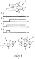
- An example of an initial complete circuit and of its subnetworks for a simple simulation is given in Figure 1, in which the reference numeral 1 designates the initial circuit to be simulated, with inputs A, B, C and an output Z.
- the example circuit is composed of a set of logic gates, and specifically a NOT gate 1, two AND gates 2 and 3, and an OR gate 4.
- the signals A, B, C and Z are shown in the charts of Figure 1 and yield the subnetworks, designated by the reference numerals 5 and 6, which represent the active devices according to the instant considered in relation to the application of the signals A, B and C.
- the subnetwork 5 is a schematic representation of the circuit 1 at the instant in which the signals A and B are nil and the signal C has a step.
- the NOT gate 1 is not present, since its input is nil, while the second input of the AND gate 3, in addition to the input C, is connected to the supply voltage, since a high signal would have been output by the NOT gate 1 with a low signal B as input.
- the second subnetwork is the circuit obtained when the signal B performs a transition from low to high while the signal C is still high.
- the NOT gate 1 is included in the subcircuit, while the input of the AND gate 3 that corresponds to the signal C is at the supply voltage, since said signal does not perform a transition but remains high, as in the situation occurring in the circuit 5.
- the circuit 1 is divided into the two subcircuits 5 and 6, which include only the devices that are active at that given instant.
- a combination of the above information leads to the extraction of the devices that are active at every instant according to the different timings of the signals.
- the devices are included in the subcircuit that must be simulated electrically if at least one of their gates is connected to a subcircuit whose value has changed.
- the dynamic time-dependent partitioning of the circuit is provided according to different methods: a fixed time interval or a time interval defined between the time elapsed between transitions of signals arriving from the testing rig and input to the circuit, or for example the ratio between active devices and all devices is considered.
- the advantage of using the signal or signals arriving from the testing rig is given by the fact that the slope of said signal is known and therefore a time interval considered to extract the active devices and thus form subcircuits composed exclusively of the active circuits, starting from the circuit to be simulated, occurs at an input transition of said signal.
- the active devices change dynamically from one time interval to the next, the state of the input/output ports of the devices is known by virtue of the digital simulator. This allows compatibility of the internal state even if one or more input nodes of the current device are not connected to any driving device.
- the nodes must become visible outside the device. For example, they might be handled as extended floating outputs (i.e., with non-connected output pin). All the output nodes, including the latter, can furthermore be initialized, obtaining a faster convergence for the DC operating point.
- the internal nodes are resolved automatically by the simulator during the evaluation of the DC operating point. Floating nodes cannot be accessed by the digital simulator. The electric simulator provides a hypothesis on the basis of its internal heuristics.
- the individual results can be concatenated together in order to compose the entire simulation.
- Simulation then entails extracting the active devices, i.e., the devices for which a digital transition has been detected, a step for evaluating the voltage that is present on the inactive nodes of the circuit and an estimate of the equivalent loads for replacing said nodes.
- Figure 2 is a table which compares various circuits listed in the first column of the table, constituted by the number of gates listed in the second column, while a third column indicates the operating time of the CPU, comparing the simulation of the full circuit and the simulation performed by means of the method according to the invention.
- the fourth column of the table lists the memory occupation of modeling performed by means of known methods in comparison with modeling performed by means of the method according to the invention.
- the fifth column lists a percentage error for the calculated average power level of the simulated circuit and the last column lists the type of circuit, which can be combinational, sequential or self-timed.
- the method according to the invention fully achieves the intended aim and objects, since it allows to split the simulation of a large circuit into a plurality of simulations of smaller independent subcircuits, each of which can be simulated electrically. In this manner, the electrical simulation is faster and can also be performed in parallel, since each circuit is independent of the other.
Landscapes
- Engineering & Computer Science (AREA)
- Computer Hardware Design (AREA)
- Physics & Mathematics (AREA)
- Theoretical Computer Science (AREA)
- Evolutionary Computation (AREA)
- Geometry (AREA)
- General Engineering & Computer Science (AREA)
- General Physics & Mathematics (AREA)
- Microelectronics & Electronic Packaging (AREA)
- Design And Manufacture Of Integrated Circuits (AREA)
- Test And Diagnosis Of Digital Computers (AREA)
- Tests Of Electronic Circuits (AREA)
Abstract
Description
Claims (10)
- A method for the electric dynamic simulation of VLSI circuits, characterized in that it comprises the steps of:-- determining, by means of a digital simulator and starting from a circuit to be simulated, a plurality of independent subcircuits whose dimensions are equal to, or smaller than, those of said circuit;-- electrically simulating each one of said subcircuits; and-- concatenating the results obtained by means of said electric simulations of the subcircuits.
- The method according to claim 1, characterized in that said step that consists in dividing said circuit into a plurality of independent subcircuits comprises the steps of:-- defining a time interval;-- extracting, for each time interval, devices of said circuit for which a digital transition is detected;-- evaluating the voltage that is present on inactive nodes of said circuit;-- estimating equivalent loads for replacing said inactive nodes.
- The method according to claim 2, characterized in that said step of using a digital simulator entails the use of said digital simulator together with an interface.
- The method according to one or more of the preceding claims, characterized in that said step of electrically simulating each one of said subcircuits is performed by means of an electric simulator.
- The method according to one or more of the preceding claims, characterized in that said devices for which a digital transition is detected are active devices, said devices being active if at least one of the gates of the device is connected to a node of the circuit that has changed value.
- The method according to one or more of the preceding claims, characterized in that each input of an active device of the circuit is connected to the supply voltage if in that given time interval the signal that is normally present at said input is high and is connected to the ground if the signal that is normally present at said input is low.
- The method according to one or more of the preceding claims, characterized in that said time interval is determined as the time elapsed between two transitions of input signals arriving from a testing rig.
- The method according to one or more of the preceding claims, characterized in that said time interval is determined as a fixed time.
- The method according to one or more of the preceding claims, characterized in that said time interval is determined by the ratio between active devices and total devices.
- The method according to one or more of the preceding claims, characterized in that said time interval is determined on the basis of statistics obtained from other preceding simulations.
Priority Applications (3)
| Application Number | Priority Date | Filing Date | Title |
|---|---|---|---|
| EP98830526A EP0986015B1 (en) | 1998-09-09 | 1998-09-09 | Method for the electric dynamic simulation of VLSI circuits |
| DE69820051T DE69820051D1 (en) | 1998-09-09 | 1998-09-09 | Process for dynamic electrical simulation of VLSI circuits |
| US09/370,514 US6539346B1 (en) | 1998-09-09 | 1999-08-06 | Method for the electric dynamic simulation of VLSI circuits |
Applications Claiming Priority (1)
| Application Number | Priority Date | Filing Date | Title |
|---|---|---|---|
| EP98830526A EP0986015B1 (en) | 1998-09-09 | 1998-09-09 | Method for the electric dynamic simulation of VLSI circuits |
Publications (2)
| Publication Number | Publication Date |
|---|---|
| EP0986015A1 true EP0986015A1 (en) | 2000-03-15 |
| EP0986015B1 EP0986015B1 (en) | 2003-11-26 |
Family
ID=8236778
Family Applications (1)
| Application Number | Title | Priority Date | Filing Date |
|---|---|---|---|
| EP98830526A Expired - Lifetime EP0986015B1 (en) | 1998-09-09 | 1998-09-09 | Method for the electric dynamic simulation of VLSI circuits |
Country Status (3)
| Country | Link |
|---|---|
| US (1) | US6539346B1 (en) |
| EP (1) | EP0986015B1 (en) |
| DE (1) | DE69820051D1 (en) |
Families Citing this family (1)
| Publication number | Priority date | Publication date | Assignee | Title |
|---|---|---|---|---|
| US7024648B1 (en) * | 1999-06-15 | 2006-04-04 | Siemens Aktiengesellschaft | Computer-assisted method for the parallel calculation of the operating point of electric circuits |
Citations (1)
| Publication number | Priority date | Publication date | Assignee | Title |
|---|---|---|---|---|
| EP0481117A1 (en) * | 1990-10-18 | 1992-04-22 | Siemens Aktiengesellschaft | Method for accelerating simulation in computer-aided design of electronic circuits and systems |
Family Cites Families (8)
| Publication number | Priority date | Publication date | Assignee | Title |
|---|---|---|---|---|
| US5572437A (en) * | 1990-04-06 | 1996-11-05 | Lsi Logic Corporation | Method and system for creating and verifying structural logic model of electronic design from behavioral description, including generation of logic and timing models |
| US5369594A (en) * | 1992-06-18 | 1994-11-29 | International Business Machines Corporation | Conjugate gradient method in computer-aided circuit design |
| US5550760A (en) * | 1993-02-18 | 1996-08-27 | Digital Equipment Corporation | Simulation of circuits |
| US5694579A (en) * | 1993-02-18 | 1997-12-02 | Digital Equipment Corporation | Using pre-analysis and a 2-state optimistic model to reduce computation in transistor circuit simulation |
| US5446676A (en) * | 1993-03-29 | 1995-08-29 | Epic Design Technology Inc. | Transistor-level timing and power simulator and power analyzer |
| US6112022A (en) * | 1996-12-13 | 2000-08-29 | Legend Design Technology, Inc. | Method for simulating ULSI/VLSI circuit designs |
| US6249901B1 (en) * | 1996-12-13 | 2001-06-19 | Legend Design Technology, Inc. | Memory characterization system |
| US6009249A (en) * | 1997-06-13 | 1999-12-28 | Micron Technology, Inc. | Automated load determination for partitioned simulation |
-
1998
- 1998-09-09 DE DE69820051T patent/DE69820051D1/en not_active Expired - Lifetime
- 1998-09-09 EP EP98830526A patent/EP0986015B1/en not_active Expired - Lifetime
-
1999
- 1999-08-06 US US09/370,514 patent/US6539346B1/en not_active Expired - Lifetime
Patent Citations (1)
| Publication number | Priority date | Publication date | Assignee | Title |
|---|---|---|---|---|
| EP0481117A1 (en) * | 1990-10-18 | 1992-04-22 | Siemens Aktiengesellschaft | Method for accelerating simulation in computer-aided design of electronic circuits and systems |
Non-Patent Citations (2)
| Title |
|---|
| DRAGONE N ET AL: "Power invariant vector compaction based on bit clustering and temporal partitioning", PROCEEDINGS. 1998 INTERNATIONAL SYMPOSIUM ON LOW POWER ELECTRONICS AND DESIGN (IEEE CAT. NO.98TH8379), PROCEEDINGS OF INTERNATIONAL SYMPOSIUM ON LOW POWER ELECTRONICS AND DESIGN, MONTEREY, CA, USA, 10-12 AUG. 1998, ISBN 1-58113-059-7, 1998, New York, NY, USA, ACM, USA, pages 118 - 120, XP002094403 * |
| FROHLICH N ET AL: "A new approach for parallel simulation of VLSI circuits on a transistor level", IEEE TRANSACTIONS ON CIRCUITS AND SYSTEMS I: FUNDAMENTAL THEORY AND APPLICATIONS, JUNE 1998, IEEE, USA, vol. 45, no. 6, ISSN 1057-7122, pages 601 - 613, XP002094404 * |
Also Published As
| Publication number | Publication date |
|---|---|
| DE69820051D1 (en) | 2004-01-08 |
| US6539346B1 (en) | 2003-03-25 |
| EP0986015B1 (en) | 2003-11-26 |
Similar Documents
| Publication | Publication Date | Title |
|---|---|---|
| EP0229975B1 (en) | Methods for the modeling and fault simulation of complementary metal oxide semiconductor circuits | |
| US6499131B1 (en) | Method for verification of crosstalk noise in a CMOS design | |
| US6363516B1 (en) | Method for hierarchical parasitic extraction of a CMOS design | |
| US7117466B2 (en) | System and method for correlated process pessimism removal for static timing analysis | |
| US6405348B1 (en) | Deep sub-micron static timing analysis in the presence of crosstalk | |
| US6499129B1 (en) | Method of estimating performance of integrated circuit designs | |
| US6523149B1 (en) | Method and system to improve noise analysis performance of electrical circuits | |
| US20040078175A1 (en) | Method and apparatus for modeling and simulating the effects of bridge defects in integrated circuits | |
| JP2006285960A (en) | Computing current in digital circuit based on accurate current model of library cell | |
| US7240304B2 (en) | Method for voltage drop analysis in integreted circuits | |
| KR100749753B1 (en) | Simulation method and apparatus at gate level, method of desiging ics, method of designing ics including voltage islands, and method of designing chips | |
| Bogiolo et al. | Power estimation of cell-based CMOS circuits | |
| US20030037306A1 (en) | Variable detail automatic invocation of transistor level timing for application specific integrated circuit static timing analysis | |
| US7747972B2 (en) | Methods and apparatuses for timing analysis of electronic circuits | |
| Zachariah et al. | On modeling cross-talk faults [VLSI circuits] | |
| Kashyap et al. | A nonlinear cell macromodel for digital applications | |
| CN113723045A (en) | Design method of digital integrated circuit | |
| US6820243B1 (en) | Hybrid system of static analysis and dynamic simulation for circuit design | |
| Santos et al. | Defect-oriented mixed-level fault simulation of digital systems-on-a-chip using HDL | |
| Santos et al. | Defect-oriented verilog fault simulation of SoC macros using a stratified fault sampling technique | |
| EP0986015B1 (en) | Method for the electric dynamic simulation of VLSI circuits | |
| Lin et al. | A power modeling and characterization method for the CMOS standard cell library | |
| Hayes | A fault simulation methodology for VLSI | |
| US6854102B1 (en) | System and method of acquiring delay, setup and hold values for integrated circuit cells | |
| US6711722B1 (en) | Method for deriving a functional circuit description |
Legal Events
| Date | Code | Title | Description |
|---|---|---|---|
| PUAI | Public reference made under article 153(3) epc to a published international application that has entered the european phase |
Free format text: ORIGINAL CODE: 0009012 |
|
| AK | Designated contracting states |
Kind code of ref document: A1 Designated state(s): DE FR GB IT |
|
| AX | Request for extension of the european patent |
Free format text: AL;LT;LV;MK;RO;SI |
|
| 17P | Request for examination filed |
Effective date: 20000825 |
|
| AKX | Designation fees paid |
Free format text: DE FR GB IT |
|
| 17Q | First examination report despatched |
Effective date: 20020221 |
|
| GRAH | Despatch of communication of intention to grant a patent |
Free format text: ORIGINAL CODE: EPIDOS IGRA |
|
| GRAS | Grant fee paid |
Free format text: ORIGINAL CODE: EPIDOSNIGR3 |
|
| GRAA | (expected) grant |
Free format text: ORIGINAL CODE: 0009210 |
|
| AK | Designated contracting states |
Kind code of ref document: B1 Designated state(s): DE FR GB IT |
|
| REG | Reference to a national code |
Ref country code: GB Ref legal event code: FG4D |
|
| REF | Corresponds to: |
Ref document number: 69820051 Country of ref document: DE Date of ref document: 20040108 Kind code of ref document: P |
|
| PG25 | Lapsed in a contracting state [announced via postgrant information from national office to epo] |
Ref country code: DE Free format text: LAPSE BECAUSE OF FAILURE TO SUBMIT A TRANSLATION OF THE DESCRIPTION OR TO PAY THE FEE WITHIN THE PRESCRIBED TIME-LIMIT Effective date: 20040227 |
|
| PG25 | Lapsed in a contracting state [announced via postgrant information from national office to epo] |
Ref country code: GB Free format text: LAPSE BECAUSE OF NON-PAYMENT OF DUE FEES Effective date: 20040909 |
|
| ET | Fr: translation filed | ||
| PLBE | No opposition filed within time limit |
Free format text: ORIGINAL CODE: 0009261 |
|
| STAA | Information on the status of an ep patent application or granted ep patent |
Free format text: STATUS: NO OPPOSITION FILED WITHIN TIME LIMIT |
|
| 26N | No opposition filed |
Effective date: 20040827 |
|
| GBPC | Gb: european patent ceased through non-payment of renewal fee |
Effective date: 20040909 |
|
| PGFP | Annual fee paid to national office [announced via postgrant information from national office to epo] |
Ref country code: IT Payment date: 20060930 Year of fee payment: 9 |
|
| PGFP | Annual fee paid to national office [announced via postgrant information from national office to epo] |
Ref country code: FR Payment date: 20070926 Year of fee payment: 10 |
|
| REG | Reference to a national code |
Ref country code: FR Ref legal event code: ST Effective date: 20090529 |
|
| PG25 | Lapsed in a contracting state [announced via postgrant information from national office to epo] |
Ref country code: IT Free format text: LAPSE BECAUSE OF NON-PAYMENT OF DUE FEES Effective date: 20070909 |
|
| PG25 | Lapsed in a contracting state [announced via postgrant information from national office to epo] |
Ref country code: FR Free format text: LAPSE BECAUSE OF NON-PAYMENT OF DUE FEES Effective date: 20080930 |