EP0984518A2 - Electrical connector for PGA package - Google Patents

Electrical connector for PGA package Download PDF

Info

Publication number
EP0984518A2
EP0984518A2 EP99117162A EP99117162A EP0984518A2 EP 0984518 A2 EP0984518 A2 EP 0984518A2 EP 99117162 A EP99117162 A EP 99117162A EP 99117162 A EP99117162 A EP 99117162A EP 0984518 A2 EP0984518 A2 EP 0984518A2
Authority
EP
European Patent Office
Prior art keywords
contact
electrical connector
housing board
pga package
cover
Prior art date
Legal status (The legal status is an assumption and is not a legal conclusion. Google has not performed a legal analysis and makes no representation as to the accuracy of the status listed.)
Withdrawn
Application number
EP99117162A
Other languages
German (de)
French (fr)
Other versions
EP0984518A3 (en
Inventor
Atsuhito Noda
Akinori Mizmura
Current Assignee (The listed assignees may be inaccurate. Google has not performed a legal analysis and makes no representation or warranty as to the accuracy of the list.)
Molex LLC
Original Assignee
Molex LLC
Priority date (The priority date is an assumption and is not a legal conclusion. Google has not performed a legal analysis and makes no representation as to the accuracy of the date listed.)
Filing date
Publication date
Application filed by Molex LLC filed Critical Molex LLC
Publication of EP0984518A2 publication Critical patent/EP0984518A2/en
Publication of EP0984518A3 publication Critical patent/EP0984518A3/en
Withdrawn legal-status Critical Current

Links

Images

Classifications

    • HELECTRICITY
    • H01ELECTRIC ELEMENTS
    • H01RELECTRICALLY-CONDUCTIVE CONNECTIONS; STRUCTURAL ASSOCIATIONS OF A PLURALITY OF MUTUALLY-INSULATED ELECTRICAL CONNECTING ELEMENTS; COUPLING DEVICES; CURRENT COLLECTORS
    • H01R13/00Details of coupling devices of the kinds covered by groups H01R12/70 or H01R24/00 - H01R33/00
    • H01R13/46Bases; Cases
    • H01R13/502Bases; Cases composed of different pieces
    • H01R13/508Bases; Cases composed of different pieces assembled by a separate clip or spring
    • HELECTRICITY
    • H01ELECTRIC ELEMENTS
    • H01RELECTRICALLY-CONDUCTIVE CONNECTIONS; STRUCTURAL ASSOCIATIONS OF A PLURALITY OF MUTUALLY-INSULATED ELECTRICAL CONNECTING ELEMENTS; COUPLING DEVICES; CURRENT COLLECTORS
    • H01R13/00Details of coupling devices of the kinds covered by groups H01R12/70 or H01R24/00 - H01R33/00
    • H01R13/02Contact members
    • H01R13/22Contacts for co-operating by abutting
    • H01R13/24Contacts for co-operating by abutting resilient; resiliently-mounted
    • HELECTRICITY
    • H01ELECTRIC ELEMENTS
    • H01RELECTRICALLY-CONDUCTIVE CONNECTIONS; STRUCTURAL ASSOCIATIONS OF A PLURALITY OF MUTUALLY-INSULATED ELECTRICAL CONNECTING ELEMENTS; COUPLING DEVICES; CURRENT COLLECTORS
    • H01R12/00Structural associations of a plurality of mutually-insulated electrical connecting elements, specially adapted for printed circuits, e.g. printed circuit boards [PCB], flat or ribbon cables, or like generally planar structures, e.g. terminal strips, terminal blocks; Coupling devices specially adapted for printed circuits, flat or ribbon cables, or like generally planar structures; Terminals specially adapted for contact with, or insertion into, printed circuits, flat or ribbon cables, or like generally planar structures
    • H01R12/50Fixed connections
    • H01R12/51Fixed connections for rigid printed circuits or like structures
    • H01R12/52Fixed connections for rigid printed circuits or like structures connecting to other rigid printed circuits or like structures
    • HELECTRICITY
    • H01ELECTRIC ELEMENTS
    • H01RELECTRICALLY-CONDUCTIVE CONNECTIONS; STRUCTURAL ASSOCIATIONS OF A PLURALITY OF MUTUALLY-INSULATED ELECTRICAL CONNECTING ELEMENTS; COUPLING DEVICES; CURRENT COLLECTORS
    • H01R12/00Structural associations of a plurality of mutually-insulated electrical connecting elements, specially adapted for printed circuits, e.g. printed circuit boards [PCB], flat or ribbon cables, or like generally planar structures, e.g. terminal strips, terminal blocks; Coupling devices specially adapted for printed circuits, flat or ribbon cables, or like generally planar structures; Terminals specially adapted for contact with, or insertion into, printed circuits, flat or ribbon cables, or like generally planar structures
    • H01R12/70Coupling devices
    • H01R12/71Coupling devices for rigid printing circuits or like structures
    • H01R12/712Coupling devices for rigid printing circuits or like structures co-operating with the surface of the printed circuit or with a coupling device exclusively provided on the surface of the printed circuit
    • H01R12/714Coupling devices for rigid printing circuits or like structures co-operating with the surface of the printed circuit or with a coupling device exclusively provided on the surface of the printed circuit with contacts abutting directly the printed circuit; Button contacts therefore provided on the printed circuit
    • HELECTRICITY
    • H01ELECTRIC ELEMENTS
    • H01RELECTRICALLY-CONDUCTIVE CONNECTIONS; STRUCTURAL ASSOCIATIONS OF A PLURALITY OF MUTUALLY-INSULATED ELECTRICAL CONNECTING ELEMENTS; COUPLING DEVICES; CURRENT COLLECTORS
    • H01R12/00Structural associations of a plurality of mutually-insulated electrical connecting elements, specially adapted for printed circuits, e.g. printed circuit boards [PCB], flat or ribbon cables, or like generally planar structures, e.g. terminal strips, terminal blocks; Coupling devices specially adapted for printed circuits, flat or ribbon cables, or like generally planar structures; Terminals specially adapted for contact with, or insertion into, printed circuits, flat or ribbon cables, or like generally planar structures
    • H01R12/70Coupling devices
    • H01R12/82Coupling devices connected with low or zero insertion force
    • H01R12/85Coupling devices connected with low or zero insertion force contact pressure producing means, contacts activated after insertion of printed circuits or like structures
    • H01R12/89Coupling devices connected with low or zero insertion force contact pressure producing means, contacts activated after insertion of printed circuits or like structures acting manually by moving connector housing parts linearly, e.g. slider
    • YGENERAL TAGGING OF NEW TECHNOLOGICAL DEVELOPMENTS; GENERAL TAGGING OF CROSS-SECTIONAL TECHNOLOGIES SPANNING OVER SEVERAL SECTIONS OF THE IPC; TECHNICAL SUBJECTS COVERED BY FORMER USPC CROSS-REFERENCE ART COLLECTIONS [XRACs] AND DIGESTS
    • Y10TECHNICAL SUBJECTS COVERED BY FORMER USPC
    • Y10STECHNICAL SUBJECTS COVERED BY FORMER USPC CROSS-REFERENCE ART COLLECTIONS [XRACs] AND DIGESTS
    • Y10S439/00Electrical connectors
    • Y10S439/91Observation aide, e.g. transparent material, window in housing

Definitions

  • the present invention relates generally to an electrical connector for a PGA package for connecting the PGA package provided with pins for connection in grid array fashion (pin grid array package, and hereinafter also referred to as "package") to a printed circuit board and so forth.
  • this type of the electrical connector for the package comprises a housing board in which a plurality of contact holes adapted for receiving the pins of the package are formed in grid array fashion, a plurality of terminals mounted on each of the contact holes, and a cover in which through holes adapted for insertion of the pins are formed in grid array fashion and slidably provided on the upper side of the housing board.
  • the cover serves for insertion of the pins into the contact holes by zero insertion force. After inserting the pins into the contacts holes of the housing board through the through holes of the cover, the cover slides to move the overall pin grid array, i.e., the package, so that the pins and the terminals are electrically engaged (For example, see Japanese Patent No. 2689325).
  • Each terminal is formed into the configuration in which a solder tail is provided on the extension of a contact piece for engaging with each pin via an engaging portion for engaging with the housing board.
  • This solder tail is usually formed into the pin shaped configuration adapted for dip soldering.
  • each terminal is formed into the configuration in which the contact piece, the engaging portion and the solder tail are continued in straight as set forth above. Therefore, it necessitates making the terminal length long, and making the thickness of the housing board generally similar to the length of the contact piece and the engaging portion to encounter the problem that reduction of the height of the overall electrical connector is difficult.
  • the present invention has been worked out in order to solve the problems set forth above. Therefore, it is an object of the present invention to provide an electrical connector for a PGA package having a structure adapted for reduction of the height thereof.
  • the present invention contemplates the provision of structure in which the contact piece and the engaging piece for engaging with the housing board are provided in parallel in place of structure of the terminal in which they are provided in straight.
  • An electrical connector for a PGA package may comprise: a housing board in which a plurality of contact holes adapted for receiving pins of the PGA package are formed in grid array fashion;
  • each terminal is formed by independently arranging respective spring contact and engaging piece in parallel. Accordingly, the length of the terminal can be shorten without sacrificing the effective spring length of the spring contact, and the housing board can be also made low-profile.
  • Fig. I is an illustration of a preferred embodiment of an electrical connector for a PGA package 1, in disassembled condition. The assembled condition is shown in Fig. 4.
  • the electrical connector for the PGA package I comprises a housing board 2, terminals 3 mounted on the housing board 2, and a cover 4 placed on the upper side of the housing board 2.
  • the housing board 2 is molded of dielectric plastic, a tin plate board as being quadrangular in a plan view.
  • a mounting portion 6 of a lever 5 for sliding the cover 4 is formed along the rear edge of the housing board.
  • Contact holes 7 passing through the housing board 2 are formed in grid array fashion over generally whole area of the other portion.
  • the contact holes 7 formed in grid array fashion are located with offset for half pitch in the adjacent rows (transverse direction in Fig. 2) as shown in Fig. 2. They are located in staggered fashion as a whole.
  • the terminal 3 is mounted within each contact hole 7.
  • the terminal 3 is stamped and formed of sheet metal, and includes a generally U-shaped spring contact 10 formed by a bottom piece 8 and a pair of contact pieces 9 and an engaging piece 11 extending in parallel with the contact pieces 9 from side of the bottom piece 8.
  • the distal end of each contact piece 9 is inwardly bulged to form a contact portion 9a.
  • a solder tail 12 is extended in parallel with the lower side of the bottom piece 8 from the other side of the bottom piece 8. As shown in Fig. 3, it is adapted for surface soldering on the surface of a printed circuit board 13.
  • engaging holes 14 are formed corresponding to the engaging pieces 11 adjacent to the contact holes 7 along the rows of the contact holes 7 (see Fig. 3).
  • Each terminal 3 is mounted from the side of the bottom surface 2a of the housing board 2, and fixed by engaging under pressure between the engaging piece 11 and the engaging hole 14.
  • the engaging piece 11 is oriented in the foregoing direction of the row relative to the spring contact 10 of the terminal 3.
  • the contact hole 7 are formed adapting to the stroke in which the cover 4 slides in the foregoing direction of the row.
  • the spring contact 10 of each terminal 3 mounted on the housing board 2 is located on one side of each contact hole 7, and a space for inserting each pin 15 (see Figs. 2, 5, and 6) of a package (not shown) by zero insertion force is provided on the other side of each contact hole 7.
  • the cover 4 is formed into the quadrangular plate configuration of which size is generally similar to that of the housing board 2 as shown in the drawings, in the preferred embodiment, the cover 4 is formed of metal sheet (aluminum, stainless steel or the like).
  • metal sheet aluminum, stainless steel or the like.
  • Engaging portions 17 with the lever 5 are formed on opposite sides of the rear edge of the cover 4.
  • through holes 18 are provided in grid array fashion corresponding to the contact holes 7 of the housing board 2.
  • the through holes 18 are adapted for insertion of the pins 15 of the package, and formed by combining counter bores 19 on the surface side and straight holes 20 on the lower surface side.
  • the rear edge portion of the cover 4 is constructed by mounting a stiffener 21 with rivets 22 in Fig. 1. However, it is formed as an integrally molded structure in Fig. 4.
  • the cover 4 formed of metal sheet is coated by insulating coating such as oxide film or the like to prevent from electrically conducting with the pins 15 inserted into the through holes 18.
  • a crank bar portion 23 and an operating portion 24 are continuous into the L-shaped configuration to form the lever 5.
  • the center section of the crank bar portion 23 is inserted into the mounting portion 6 of the housing board 2, and opposite end portions thereof are inserted into elongated holes 25 formed in the engaging portions 17 of the cover 4.
  • the reference numeral 26 denotes a snap ring.
  • a plurality of the through holes 18 are formed in the cover 4 in grid array fashion. However, in the portion where the through holes are essentially formed, some portions are left as blanks 28 without forming the through holes in grid array fashion. Furthermore, portions 29 in which no contact hole 7 is formed are also left in the housing board 2 corresponding to the blank portions 28. On the side of the bottom surface 2a of each portion 29 in which no contact hole is formed, a projection 30 is formed as shown in Figs. 2 and 3 . A nail portion 32 of a compliant pin 31 is engaged under pressure with each projection 30 from the side of the bottom surface 2a, and the compliant pin 31 is projected from the bottom surface 2a of the housing board 2.
  • Fig. 3 is an illustration showing the condition where the foregoing preferred embodiment of the electrical connector for the PGA package 1 is mounted on the printed circuit board 13.
  • Each compliant pin 31 projecting from the bottom surface 2a of the housing board 2 is engaged with an engaging hole 33 of the printed circuit board 13.
  • the solder tails 12 of the terminals 3 arranged in staggered fashion along the bottom surface 2a of the housing board 2 surface soldered to circuit pads (not shown) of the printed circuit board 13.
  • Figs. 5 and 6 are illustrations showing the relative position of the cover 4 relative to the housing board 2 and the terminals 3 in the risen and fallen positions of the operating portion 24 of the lever 5.
  • Fig. 5 is an illustration showing the condition in the fallen position of the operating portion 24.
  • the cover 4 is slidingly moved as indicated by arrow 16a to move to the position where the through hole 18 of the cover 4 is matched with the spring contact 10 of the terminal 3.
  • Fig. 6 is an illustration showing the condition in the risen position of the operating portion 24.
  • the cover 4 slides as indicated by arrow 16b to move the through hole 18 to the position corresponding to the side of the spring contact 10.
  • the package When the package is connected to the printed circuit board 13 via the electrical connector for the PGA package 1, the package is placed on the cover 4 after the operating portion 24 of the lever 5 is risen, and the pins 15 are inserted into the contact holes 7 via the through holes 18 of the cover 4. Each pin 15 is entered into the side of the spring contact 10 of each terminal 3 to be inserted by zero insertion force.
  • Each terminal 3 is formed by independently arranging respective spring contact 10 and engaging piece 11 in parallel. Therefore, the contact pieces 9 can achieve the spring characteristics by defining the overall length generally similar to the thickness of the housing board 2 as the effective spring length, and establish certain electrical conduction between the pins 15.
  • the overall length of the effective spring length of the contact piece 9 can be made generally similar to the thickness of the housing board 2, the length of the contact piece 9 and the thickness of the housing board 2 can be reduced as long as spring performance necessary for electrical conduction can be provided. Therefore reduction of height of the electrical connector for the package I can be achieved. Furthermore, by shortening length of the contact piece 9, the inductance of the terminals 3 can be made small to contribute to the high speed communication of the signal. It should be noted that the cover 4 formed of metal sheet also contributes to reduction of height of the electrical connector for the PGA package 1 Because, the cover 4 can provide necessary strength as the cover, even if it is formed of thin plate.
  • the operating portion 24 of the lever 5 Upon releasing the connection condition of the package, the operating portion 24 of the lever 5 is to be risen, when the operating portion 24 is risen, the pins 15 are moved to the side of the spring contacts 10 as indicated by arrow 16b in Fig. 6 to remove the package without necessitating large withdrawal. Again, the compliant pins 31 can protect the soldering portions of the solder tails 12.
  • the contact piece 10 of each terminal 3 is formed into the generally U-shaped configuration by the bottom piece 8 and a pair of the contact pieces 9, but not limited to this configuration. It may also be constructed such that one contact piece is provided to be pressed each pin 15 thereinto.
  • each pin 15 is clamped by a pair of the contact pieces 9 as set forth in the preferred embodiment, there is no relationship between the stress due to slide of the cover 4 and electrical conducting condition to establish certain conduction.
  • solder tail 12 of each terminal 3 is also not limited to the configuration adapted for surface soldering.
  • the pin shaped solder tails may be inserted into the through holes of the printed circuit board 13 and soldered by dip method
  • the arrangement density of the compliant pins 31 is set in consideration of the stress exerted on the terminals 3 and the housing board 2 by sliding the cover 4. It is considered to be suitable that they are distributed in the density of about one tenth of arrangement density of the terminals 3.
  • each terminal is formed by independently arranging respective spring contact and engaging piece in parallel, the length of the terminal can be shorten, and the housing board can be also made low-profile by providing the effective spring length of each spring contact to the extent necessary for electrical conduction between the pins of the package. Accordingly reduction of the height of the electrical connector for PGA package can be achieved.
  • Each pin of the package is clamped by a pair of the contact pieces to establish certain electrical conduction.
  • the electrical connector for the PGA package adapted for mounting on printed circuit board by surface soldering.
  • the compliance pins can resist the stress exerted on the terminals and the housing board by sliding the cover to protect the soldering portions of the solder tails.

Abstract

An electrical connector for a PGA package is provided for reduction of the height thereof. An electrical connector for a PGA package comprises a housing board in which a plurality of contact holes adapted for receiving pins of the PGA package formed in grid array fashion, a plurality of terminals mounted within each of the contact holes, and a cover in which through holes adapted for insertion of the pins are formed in grid array fashion, and slidably provided on the upper side of the housing board. Each of the terminals is located within contact holes, and formed by independently arranging respective spring contact adapted for electrical engagement with the pin and engaging piece engaged under pressure from a bottom surface of the housing board in parallel <IMAGE>

Description

Field of the Invention
The present invention relates generally to an electrical connector for a PGA package for connecting the PGA package provided with pins for connection in grid array fashion (pin grid array package, and hereinafter also referred to as "package") to a printed circuit board and so forth.
Description of the Related Art
Conventionally, this type of the electrical connector for the package comprises a housing board in which a plurality of contact holes adapted for receiving the pins of the package are formed in grid array fashion, a plurality of terminals mounted on each of the contact holes, and a cover in which through holes adapted for insertion of the pins are formed in grid array fashion and slidably provided on the upper side of the housing board. The cover serves for insertion of the pins into the contact holes by zero insertion force. After inserting the pins into the contacts holes of the housing board through the through holes of the cover, the cover slides to move the overall pin grid array, i.e., the package, so that the pins and the terminals are electrically engaged (For example, see Japanese Patent No. 2689325).
Each terminal is formed into the configuration in which a solder tail is provided on the extension of a contact piece for engaging with each pin via an engaging portion for engaging with the housing board. This solder tail is usually formed into the pin shaped configuration adapted for dip soldering.
With the typical electrical connector for the PGA package, each terminal is formed into the configuration in which the contact piece, the engaging portion and the solder tail are continued in straight as set forth above. Therefore, it necessitates making the terminal length long, and making the thickness of the housing board generally similar to the length of the contact piece and the engaging portion to encounter the problem that reduction of the height of the overall electrical connector is difficult.
Summary of the Invention
The present invention has been worked out in order to solve the problems set forth above. Therefore, it is an object of the present invention to provide an electrical connector for a PGA package having a structure adapted for reduction of the height thereof.
To accomplish the above-mentioned object, the present invention contemplates the provision of structure in which the contact piece and the engaging piece for engaging with the housing board are provided in parallel in place of structure of the terminal in which they are provided in straight.
An electrical connector for a PGA package may comprise: a housing board in which a plurality of contact holes adapted for receiving pins of the PGA package are formed in grid array fashion;
  • a plurality of terminals mounted within each of the contact holes;
  • a cover in which through holes adapted for insertion of the pins are formed in grid array fashion, and slidably provided on the upper side of the housing board; and
  • each of the terminals being located within the contact holes, and formed by independently arranging respective spring contact adapted for electrical engagement with the pin and engaging piece engaged under pressure from a bottom surface of the housing board in parallel.
  • With the electrical connector for the PGA package according to the present invention, each terminal is formed by independently arranging respective spring contact and engaging piece in parallel. Accordingly, the length of the terminal can be shorten without sacrificing the effective spring length of the spring contact, and the housing board can be also made low-profile.
    Brief description of the drawings
    The present invention will be understood more fully from detailed description given herebelow and from the accompanying drawings of the preferred embodiment of the present invention, which, however, should not be taken to be limitative to the invention, but are for explanation and understanding only.
    In the drawings:
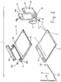
  • Fig. 1 is an exploded perspective view of a preferred embodiment of an electrical connector for a PGA package according to the present invention;
  • Fig. 2 is a partially enlarged top plan view of the preferred embodiment of a housing board according to the present invention;
  • Fig. 3 is a partially enlarged section showing the condition where the preferred embodiment of the electrical connector for the PGA package is mounted on a printed
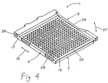
 circuit board;
  • Fig. 4 is a perspective view of the preferred embodiment of the electrical connector for the PGA package according to the present invention;
  • Fig. 5 is an illustration explaining the relative position of a cover relative to the housing board and a terminal, in the fallen position of an operating portion of the lever; and
  • Fig. 6 is an illustration explaining the relative position of a cover relative to the housing board and the terminal, in the risen position of an operating portion of the lever.
  • Description of the Preferred Embodiment
    The present invention will be discussed hereinafter in detail in terms of the preferred embodiment of the present invention with reference to the accompanying drawings. In the following description, numerous specific details are set forth in order to provide a thorough understanding of the present invention. It will be obvious, however, to those skilled in the art that the present invention may be practiced without these specific details. In other instance, well-known structures are not shown in detail in order to avoid unnecessarily obscure the present invention.
    Fig. I is an illustration of a preferred embodiment of an electrical connector for a PGA package 1, in disassembled condition. The assembled condition is shown in Fig. 4. The electrical connector for the PGA package I comprises a housing board 2, terminals 3 mounted on the housing board 2, and a cover 4 placed on the upper side of the housing board 2.
    The housing board 2 is molded of dielectric plastic, a tin plate board as being quadrangular in a plan view. A mounting portion 6 of a lever 5 for sliding the cover 4 is formed along the rear edge of the housing board. Contact holes 7 passing through the housing board 2 are formed in grid array fashion over generally whole area of the other portion. The contact holes 7 formed in grid array fashion are located with offset for half pitch in the adjacent rows (transverse direction in Fig. 2) as shown in Fig. 2. They are located in staggered fashion as a whole. By this arrangement, it becomes possible to make the distance A indicated in Fig. 2 as short as possible (for example, 1.2 7mm).
    The terminal 3 is mounted within each contact hole 7. The terminal 3 is stamped and formed of sheet metal, and includes a generally U-shaped spring contact 10 formed by a bottom piece 8 and a pair of contact pieces 9 and an engaging piece 11 extending in parallel with the contact pieces 9 from side of the bottom piece 8. The distal end of each contact piece 9 is inwardly bulged to form a contact portion 9a. Furthermore, a solder tail 12 is extended in parallel with the lower side of the bottom piece 8 from the other side of the bottom piece 8. As shown in Fig. 3, it is adapted for surface soldering on the surface of a printed circuit board 13.
    In a bottom surface 2a of the housing board 2, engaging holes 14 are formed corresponding to the engaging pieces 11 adjacent to the contact holes 7 along the rows of the contact holes 7 (see Fig. 3). Each terminal 3 is mounted from the side of the bottom surface 2a of the housing board 2, and fixed by engaging under pressure between the engaging piece 11 and the engaging hole 14. The engaging piece 11 is oriented in the foregoing direction of the row relative to the spring contact 10 of the terminal 3. The contact hole 7 are formed adapting to the stroke in which the cover 4 slides in the foregoing direction of the row. As a result, the spring contact 10 of each terminal 3 mounted on the housing board 2 is located on one side of each contact hole 7, and a space for inserting each pin 15 (see Figs. 2, 5, and 6) of a package (not shown) by zero insertion force is provided on the other side of each contact hole 7.
    Next, the cover 4 is formed into the quadrangular plate configuration of which size is generally similar to that of the housing board 2 as shown in the drawings, in the preferred embodiment, the cover 4 is formed of metal sheet (aluminum, stainless steel or the like). By forming the cover 4 with the side edge portion formed into channel shaped configuration in cross section as shown in Fig. 1, or with the side edge portion formed into reversed L-shaped configuration in cross section as shown in Fig. 4 for engaging with the side edge of the housing board 2, it is adapted for guiding the cover 4 to slide in the direction of arrow 16 by operating the lever 5.
    Engaging portions 17 with the lever 5 are formed on opposite sides of the rear edge of the cover 4. On a generally whole area of the cover 4, through holes 18 are provided in grid array fashion corresponding to the contact holes 7 of the housing board 2. The through holes 18 are adapted for insertion of the pins 15 of the package, and formed by combining counter bores 19 on the surface side and straight holes 20 on the lower surface side. The rear edge portion of the cover 4 is constructed by mounting a stiffener 21 with rivets 22 in Fig. 1. However, it is formed as an integrally molded structure in Fig. 4. The cover 4 formed of metal sheet is coated by insulating coating such as oxide film or the like to prevent from electrically conducting with the pins 15 inserted into the through holes 18.
    As shown in Fig. 1, a crank bar portion 23 and an operating portion 24 are continuous into the L-shaped configuration to form the lever 5. The center section of the crank bar portion 23 is inserted into the mounting portion 6 of the housing board 2, and opposite end portions thereof are inserted into elongated holes 25 formed in the engaging portions 17 of the cover 4. The reference numeral 26 denotes a snap ring. By rise and fall of the operating portion 24 of the lever 5 as indicated by arrow 27 of Fig. 4, the cover 4 can slid in the back and forth direction as indicated by arrow 16. This sliding direction is made consistent wit the rows of the contact holes 7 and the terminals 3.
    As set forth above, a plurality of the through holes 18 are formed in the cover 4 in grid array fashion. However, in the portion where the through holes are essentially formed, some portions are left as blanks 28 without forming the through holes in grid array fashion. Furthermore, portions 29 in which no contact hole 7 is formed are also left in the housing board 2 corresponding to the blank portions 28. On the side of the bottom surface 2a of each portion 29 in which no contact hole is formed, a projection 30 is formed as shown in Figs. 2 and 3 . A nail portion 32 of a compliant pin 31 is engaged under pressure with each projection 30 from the side of the bottom surface 2a, and the compliant pin 31 is projected from the bottom surface 2a of the housing board 2.
    Fig. 3 is an illustration showing the condition where the foregoing preferred embodiment of the electrical connector for the PGA package 1 is mounted on the printed circuit board 13. Each compliant pin 31 projecting from the bottom surface 2a of the housing board 2 is engaged with an engaging hole 33 of the printed circuit board 13. In conjunction therewith, the solder tails 12 of the terminals 3 arranged in staggered fashion along the bottom surface 2a of the housing board 2 surface soldered to circuit pads (not shown) of the printed circuit board 13.
    Figs. 5 and 6 are illustrations showing the relative position of the cover 4 relative to the housing board 2 and the terminals 3 in the risen and fallen positions of the operating portion 24 of the lever 5. Namely, Fig. 5 is an illustration showing the condition in the fallen position of the operating portion 24. The cover 4 is slidingly moved as indicated by arrow 16a to move to the position where the through hole 18 of the cover 4 is matched with the spring contact 10 of the terminal 3. Fig. 6 is an illustration showing the condition in the risen position of the operating portion 24. The cover 4 slides as indicated by arrow 16b to move the through hole 18 to the position corresponding to the side of the spring contact 10.
    When the package is connected to the printed circuit board 13 via the electrical connector for the PGA package 1, the package is placed on the cover 4 after the operating portion 24 of the lever 5 is risen, and the pins 15 are inserted into the contact holes 7 via the through holes 18 of the cover 4. Each pin 15 is entered into the side of the spring contact 10 of each terminal 3 to be inserted by zero insertion force.
    Next, when the operating portion 24 of the lever 5 is fallen, the cover 4 slides in the direction of arrow 16a of Fig. 5. Accordingly, the pins 15 and the overall package slide in the identical direction, so that each pin 15 is moved to the position of the spring contact 10 of the corresponding terminal 3. As a result, the pins 15 are engaged with the contact portions 9a of the contacts 9 to be electrically conducted, and placed into the condition where they are connected with the circuit of the printed circuit board 13 via the terminals 3.
    Each terminal 3 is formed by independently arranging respective spring contact 10 and engaging piece 11 in parallel. Therefore, the contact pieces 9 can achieve the spring characteristics by defining the overall length generally similar to the thickness of the housing board 2 as the effective spring length, and establish certain electrical conduction between the pins 15.
    Furthermore, since the overall length of the effective spring length of the contact piece 9 can be made generally similar to the thickness of the housing board 2, the length of the contact piece 9 and the thickness of the housing board 2 can be reduced as long as spring performance necessary for electrical conduction can be provided. Therefore reduction of height of the electrical connector for the package I can be achieved. Furthermore, by shortening length of the contact piece 9, the inductance of the terminals 3 can be made small to contribute to the high speed communication of the signal. It should be noted that the cover 4 formed of metal sheet also contributes to reduction of height of the electrical connector for the PGA package 1 Because, the cover 4 can provide necessary strength as the cover, even if it is formed of thin plate.
    When the pins 15 of the package are moved on the side of the spring contacts 10 of the terminals 3 by operating the lever 5 as set forth above, the stress is exerted in the sliding direction relative to the terminals 3 and the housing board 2. The compliant pins 31 engaged with the printed circuit board 13 can mainly resist this stress.
    Accordingly, it becomes possible to prevent the excessive stress from acting on soldering portions of the solder tails 12 of the terminals 3, and causing the incomplete connection such as peel of f of the soldering portions and so forth.
    Upon releasing the connection condition of the package, the operating portion 24 of the lever 5 is to be risen, when the operating portion 24 is risen, the pins 15 are moved to the side of the spring contacts 10 as indicated by arrow 16b in Fig. 6 to remove the package without necessitating large withdrawal. Again, the compliant pins 31 can protect the soldering portions of the solder tails 12.
    In the foregoing preferred embodiment, the contact piece 10 of each terminal 3 is formed into the generally U-shaped configuration by the bottom piece 8 and a pair of the contact pieces 9, but not limited to this configuration. It may also be constructed such that one contact piece is provided to be pressed each pin 15 thereinto.
    With the construction in which each pin 15 is clamped by a pair of the contact pieces 9 as set forth in the preferred embodiment, there is no relationship between the stress due to slide of the cover 4 and electrical conducting condition to establish certain conduction.
    Furthermore, the solder tail 12 of each terminal 3 is also not limited to the configuration adapted for surface soldering. The pin shaped solder tails may be inserted into the through holes of the printed circuit board 13 and soldered by dip method The arrangement density of the compliant pins 31 is set in consideration of the stress exerted on the terminals 3 and the housing board 2 by sliding the cover 4. It is considered to be suitable that they are distributed in the density of about one tenth of arrangement density of the terminals 3.
    In the construction as set forth above, since each terminal is formed by independently arranging respective spring contact and engaging piece in parallel, the length of the terminal can be shorten, and the housing board can be also made low-profile by providing the effective spring length of each spring contact to the extent necessary for electrical conduction between the pins of the package. Accordingly reduction of the height of the electrical connector for PGA package can be achieved.
    Each pin of the package is clamped by a pair of the contact pieces to establish certain electrical conduction.
    Furthermore, it is possible to provide the electrical connector for the PGA package adapted for mounting on printed circuit board by surface soldering. Still further, the compliance pins can resist the stress exerted on the terminals and the housing board by sliding the cover to protect the soldering portions of the solder tails.
    Although the present invention has been illustrated and described with respect to exemplary embodiment thereof, it should be understood by those skilled in the art that the foregoing and various other changes, omissions and additions may be made therein and thereto, without departing from the spirit and scope of the present invention. Therefore, present invention should not be understood as limited to the specific embodiment set out above but to include all possible embodiments which can be embodied within a scope encompassed and equivalents thereof with respect to the feature set in the appended claims.

    Claims (4)

    1. An electrical connector for a PGA package comprising: a housing board in which a plurality of contact holes adapted for receiving pins of said PGA package are formed in grid array fashion;
      a plurality of terminals mounted within each of said contact holes; a cover in which through holes adapted for insertion of said pins are formed in grid array fashion, and slidably provided on the upper side of said housing board; and
      each of said terminals being located within said contact holes, and formed by independently arranging respective spring contact adapted for electrical engagement with said pin and engaging piece engaged under pressure from a bottom surface of said housing board in parallel.
    2. An electrical connector for a PGA package as set forth in claim 1, wherein each of said terminals includes a generally U-shaped spring contact consisting of a bottom piece and a pair of contact pieces and said engaging piece extending in parallel with said contact pieces from one side of said bottom piece.
    3. An electrical connector for a PGA package as set forth in claim 2, wherein each of said terminals includes a solder tail adapted for surface soldering extending from said bottom piece constructing said spring contact, and projecting from said bottom surface of said housing board.
    4. An electrical connector for a PGA package as set forth in any one of claims 1 to 3, wherein said housing board further includes a compliant pin projecting from said bottom surface.
    EP99117162A 1998-09-04 1999-09-01 Electrical connector for PGA package Withdrawn EP0984518A3 (en)

    Applications Claiming Priority (2)

    Application Number Priority Date Filing Date Title
    JP10267275A JP2000082555A (en) 1998-09-04 1998-09-04 Connector for pga package
    JP26727598 1998-09-04

    Publications (2)

    Publication Number Publication Date
    EP0984518A2 true EP0984518A2 (en) 2000-03-08
    EP0984518A3 EP0984518A3 (en) 2001-06-13

    Family

    ID=17442582

    Family Applications (3)

    Application Number Title Priority Date Filing Date
    EP99117162A Withdrawn EP0984518A3 (en) 1998-09-04 1999-09-01 Electrical connector for PGA package
    EP99117229A Withdrawn EP0984519A3 (en) 1998-09-04 1999-09-02 Low profile electrical connector for a PGA package and terminals therefor
    EP99117230A Withdrawn EP0984520A3 (en) 1998-09-04 1999-09-02 Inspectable electrical connector for PGA package

    Family Applications After (2)

    Application Number Title Priority Date Filing Date
    EP99117229A Withdrawn EP0984519A3 (en) 1998-09-04 1999-09-02 Low profile electrical connector for a PGA package and terminals therefor
    EP99117230A Withdrawn EP0984520A3 (en) 1998-09-04 1999-09-02 Inspectable electrical connector for PGA package

    Country Status (8)

    Country Link
    US (2) US6287137B1 (en)
    EP (3) EP0984518A3 (en)
    JP (1) JP2000082555A (en)
    KR (3) KR100344051B1 (en)
    CN (3) CN1132268C (en)
    MY (1) MY122395A (en)
    SG (3) SG82018A1 (en)
    TW (3) TW424985U (en)

    Cited By (1)

    * Cited by examiner, † Cited by third party
    Publication number Priority date Publication date Assignee Title
    CN104485540A (en) * 2014-12-24 2015-04-01 常熟市斯佳登电器有限公司 Demountable power plug

    Families Citing this family (19)

    * Cited by examiner, † Cited by third party
    Publication number Priority date Publication date Assignee Title
    JP3470314B2 (en) * 1999-07-05 2003-11-25 日本航空電子工業株式会社 ZIF connector
    US6386892B1 (en) * 2001-11-21 2002-05-14 Speed Tech Corp. Tin paste overflow-protective electric connector
    US6527577B1 (en) * 2001-12-07 2003-03-04 Hon Hai Precision Ind. Co., Ltd. CPU socket having separate retention member
    US6475012B1 (en) * 2001-12-18 2002-11-05 Hon Hai Precision Ind. Co., Ltd. Device for CPU socket actuation
    US6471536B1 (en) * 2001-12-19 2002-10-29 Hon Hai Precision Ind. Co., Ltd. Zero Insertion Force socket having mechanical fastening device
    TW525837U (en) * 2002-03-08 2003-03-21 Hon Hai Prec Ind Co Ltd Electrical connector
    US20040127085A1 (en) * 2002-10-18 2004-07-01 James Chen Connector for a pin grid array integrated circuit device
    US20040110050A1 (en) * 2002-12-09 2004-06-10 Abd Elhamid Mahmoud H Environmentally friendly and inexpensive dielectric coolant for fuel cell stacks
    US6857889B1 (en) * 2003-09-26 2005-02-22 General Motors Corporation Vehicle body to chassis connection and method
    JP4537732B2 (en) * 2004-03-04 2010-09-08 住友電装株式会社 Board connector
    JP2005294163A (en) * 2004-04-02 2005-10-20 Jst Mfg Co Ltd Electric connector with reinforcement tab
    CN2752992Y (en) * 2004-11-27 2006-01-18 番禺得意精密电子工业有限公司 Electric connector
    US7056130B1 (en) * 2005-02-09 2006-06-06 Tyco Electronics Corporation Socket connector with inspection datum windows
    FR2898734B1 (en) * 2006-03-17 2011-11-18 Abb Entrelec Sas CONNECTOR FORMING A COMPONENT FOR SURFACE MOUNTING
    CN200959472Y (en) * 2006-09-15 2007-10-10 富士康(昆山)电脑接插件有限公司 Electric connector
    US7371100B1 (en) * 2007-02-06 2008-05-13 Hon Hai Precision Ind. Co., Ltd. Fastening structure for integrated circuit and electrical connector using same
    US20090227124A1 (en) * 2008-03-06 2009-09-10 Cinch Connectors, Inc. Electrical connector
    US8367942B2 (en) * 2009-10-27 2013-02-05 Hon Hai Precision Ind. Co., Ltd. Low profile electrical interposer of woven structure and method of making same
    CN102723633A (en) * 2012-06-12 2012-10-10 上海市电力公司 Plug for plugging-unplugging type electric meter

    Citations (2)

    * Cited by examiner, † Cited by third party
    Publication number Priority date Publication date Assignee Title
    GB2295734A (en) * 1994-10-11 1996-06-05 Methode Electronics Inc Zero insertion force socket
    US5722848A (en) * 1995-10-25 1998-03-03 Hon Hai Precision Ind. Co., Ltd. Retention mechanism for self-securement of ZIF PGA socket

    Family Cites Families (21)

    * Cited by examiner, † Cited by third party
    Publication number Priority date Publication date Assignee Title
    US4059323A (en) * 1976-05-13 1977-11-22 International Business Machines Corporation Apparatus for interconnecting plural mating members
    US4221446A (en) * 1978-10-02 1980-09-09 The Bendix Corporation Electrical connector assembly
    US4498725A (en) * 1982-06-02 1985-02-12 Amp Incorporated Electrical connector
    JPS59144893U (en) * 1983-03-17 1984-09-27 日本航空電子工業株式会社 Transverse axis movement connector
    US5057031A (en) * 1990-08-15 1991-10-15 Aries Electronics, Inc. Zero insertion force pin grid array test socket
    US5092789A (en) * 1990-08-15 1992-03-03 Aries Electronics, Inc. Electrical connector for ZIF PGA test socket
    JPH0555438A (en) * 1991-08-26 1993-03-05 Rohm Co Ltd Lead terminal structure of electronic component
    US5256080A (en) * 1992-06-12 1993-10-26 The Whitaker Corporation Bail actuated ZIF socket
    US5456613A (en) * 1993-07-16 1995-10-10 Tongrand Limited Zero insertion force connector and contact therein
    JPH0730466U (en) * 1993-11-08 1995-06-06 住友電装株式会社 Female terminal fittings for connectors
    CA2115403C (en) * 1994-02-10 1998-08-04 Fu-Yu Hsu Electrical connector with zif socket
    US5443591A (en) * 1994-05-24 1995-08-22 Tsai; Tien C. Connector socket
    US5588861A (en) * 1994-07-15 1996-12-31 Berg Technology, Inc. ZIF chip socket
    US5597320A (en) * 1995-01-03 1997-01-28 Molex Incorporated Zero insertion force electrical connector and terminal
    US5622514A (en) * 1995-06-30 1997-04-22 The Whitaker Corporation Coverless pin grid array socket
    US5535513A (en) * 1995-08-25 1996-07-16 The Whitaker Corporation Method for making surface mountable connectors
    US5679020A (en) * 1995-09-29 1997-10-21 Hon Hai Precision Ind. Co., Ltd. Stopper for use with ZIF PGA socket
    US5692920A (en) * 1995-12-14 1997-12-02 Molex Incorporated Zero insertion force electrical connector and terminal
    US5697803A (en) * 1996-06-20 1997-12-16 The Whitaker Corporation ZIF socket with hold open mechanism
    JP3656175B2 (en) * 1996-10-09 2005-06-08 日本航空電子工業株式会社 Connector drive lever mounting structure
    US5762505A (en) * 1996-12-02 1998-06-09 Hon Hai Precision Ind. Co., Ltd. Alignment device for use with a socket connector

    Patent Citations (2)

    * Cited by examiner, † Cited by third party
    Publication number Priority date Publication date Assignee Title
    GB2295734A (en) * 1994-10-11 1996-06-05 Methode Electronics Inc Zero insertion force socket
    US5722848A (en) * 1995-10-25 1998-03-03 Hon Hai Precision Ind. Co., Ltd. Retention mechanism for self-securement of ZIF PGA socket

    Cited By (1)

    * Cited by examiner, † Cited by third party
    Publication number Priority date Publication date Assignee Title
    CN104485540A (en) * 2014-12-24 2015-04-01 常熟市斯佳登电器有限公司 Demountable power plug

    Also Published As

    Publication number Publication date
    US6325655B1 (en) 2001-12-04
    KR100344048B1 (en) 2002-07-22
    KR100344051B1 (en) 2002-07-22
    KR20000022916A (en) 2000-04-25
    EP0984518A3 (en) 2001-06-13
    TW427570U (en) 2001-03-21
    SG82018A1 (en) 2001-07-24
    CN1132276C (en) 2003-12-24
    US6287137B1 (en) 2001-09-11
    KR100344050B1 (en) 2002-07-19
    CN1248807A (en) 2000-03-29
    EP0984520A3 (en) 2001-06-13
    EP0984519A3 (en) 2001-06-13
    CN1247395A (en) 2000-03-15
    CN1139154C (en) 2004-02-18
    SG87825A1 (en) 2002-04-16
    TW424985U (en) 2001-03-01
    JP2000082555A (en) 2000-03-21
    CN1248806A (en) 2000-03-29
    TW421331U (en) 2001-02-01
    KR20000022914A (en) 2000-04-25
    CN1132268C (en) 2003-12-24
    MY122395A (en) 2006-04-29
    KR20000022915A (en) 2000-04-25
    EP0984519A2 (en) 2000-03-08
    EP0984520A2 (en) 2000-03-08
    SG83149A1 (en) 2001-09-18

    Similar Documents

    Publication Publication Date Title
    EP0984518A2 (en) Electrical connector for PGA package
    US4708415A (en) Electrical connectors
    US4275944A (en) Miniature connector receptacles employing contacts with bowed tines and parallel mounting arms
    US7179126B2 (en) Electrical connector with improved terminals
    US7229298B2 (en) Electrical connector having an improved grounding path
    US6821158B2 (en) Connector
    US6261113B1 (en) Electrical connector having improved arrangement of terminals
    US7229315B2 (en) Electrical connector having a shielding shell
    US20060116007A1 (en) Socket connector for carrying integrated circuit package
    US6074226A (en) Assembly of an electrical connector and ejector unit for connecting IC cards to printed circuit boards
    US5921785A (en) Electrical connector for flat cables
    US6957987B2 (en) Socket connector for integrated circuit
    US20050037642A1 (en) Electrical connector
    US7247054B2 (en) Electrical card connector
    JPH07272793A (en) Card connector and its card discharge mechanism
    US5597320A (en) Zero insertion force electrical connector and terminal
    US5791929A (en) Zero insertion force electrical connector and terminal
    US6554634B1 (en) Electrical contact for ZIF socket connector
    US6558200B1 (en) Card edge connector with commoning contacts and individual contacts and method making the same
    US20070254507A1 (en) Electrical connector with improved contacts
    US6471535B1 (en) Electrical socket
    US6558173B1 (en) Card edge connector with commoning contacts and individual contacts and method making the same
    US6776664B1 (en) Electrical connector with retention and guiding means
    US4202595A (en) Electrical connector
    US6773273B2 (en) Electrical card connector assembly

    Legal Events

    Date Code Title Description
    PUAI Public reference made under article 153(3) epc to a published international application that has entered the european phase

    Free format text: ORIGINAL CODE: 0009012

    AK Designated contracting states

    Kind code of ref document: A2

    Designated state(s): AT BE CH CY DE DK ES FI FR GB GR IE IT LI LU MC NL PT SE

    AX Request for extension of the european patent

    Free format text: AL;LT;LV;MK;RO;SI

    PUAL Search report despatched

    Free format text: ORIGINAL CODE: 0009013

    AK Designated contracting states

    Kind code of ref document: A3

    Designated state(s): AT BE CH CY DE DK ES FI FR GB GR IE IT LI LU MC NL PT SE

    AX Request for extension of the european patent

    Free format text: AL;LT;LV;MK;RO;SI

    AKX Designation fees paid
    REG Reference to a national code

    Ref country code: DE

    Ref legal event code: 8566

    STAA Information on the status of an ep patent application or granted ep patent

    Free format text: STATUS: THE APPLICATION IS DEEMED TO BE WITHDRAWN

    18D Application deemed to be withdrawn

    Effective date: 20011214