EP0982802B1 - Arrangement d'alimentation dipôle pour une antenne à réflecteur - Google Patents
Arrangement d'alimentation dipôle pour une antenne à réflecteur Download PDFInfo
- Publication number
- EP0982802B1 EP0982802B1 EP99401951A EP99401951A EP0982802B1 EP 0982802 B1 EP0982802 B1 EP 0982802B1 EP 99401951 A EP99401951 A EP 99401951A EP 99401951 A EP99401951 A EP 99401951A EP 0982802 B1 EP0982802 B1 EP 0982802B1
- Authority
- EP
- European Patent Office
- Prior art keywords
- parabolic reflector
- feed arrangement
- dipole
- arrangement
- dipole feed
- Prior art date
- Legal status (The legal status is an assumption and is not a legal conclusion. Google has not performed a legal analysis and makes no representation as to the accuracy of the status listed.)
- Expired - Lifetime
Links
Images
Classifications
-
- H—ELECTRICITY
- H01—ELECTRIC ELEMENTS
- H01Q—ANTENNAS, i.e. RADIO AERIALS
- H01Q19/00—Combinations of primary active antenna elements and units with secondary devices, e.g. with quasi-optical devices, for giving the antenna a desired directional characteristic
- H01Q19/10—Combinations of primary active antenna elements and units with secondary devices, e.g. with quasi-optical devices, for giving the antenna a desired directional characteristic using reflecting surfaces
- H01Q19/12—Combinations of primary active antenna elements and units with secondary devices, e.g. with quasi-optical devices, for giving the antenna a desired directional characteristic using reflecting surfaces wherein the surfaces are concave
- H01Q19/13—Combinations of primary active antenna elements and units with secondary devices, e.g. with quasi-optical devices, for giving the antenna a desired directional characteristic using reflecting surfaces wherein the surfaces are concave the primary radiating source being a single radiating element, e.g. a dipole, a slot, a waveguide termination
- H01Q19/134—Rear-feeds; Splash plate feeds
-
- H—ELECTRICITY
- H01—ELECTRIC ELEMENTS
- H01Q—ANTENNAS, i.e. RADIO AERIALS
- H01Q9/00—Electrically-short antennas having dimensions not more than twice the operating wavelength and consisting of conductive active radiating elements
- H01Q9/04—Resonant antennas
- H01Q9/16—Resonant antennas with feed intermediate between the extremities of the antenna, e.g. centre-fed dipole
- H01Q9/28—Conical, cylindrical, cage, strip, gauze, or like elements having an extended radiating surface; Elements comprising two conical surfaces having collinear axes and adjacent apices and fed by two-conductor transmission lines
- H01Q9/285—Planar dipole
Definitions
- This invention relates to antennas of the type having a parabolic reflector element for concentrating microwave radiation, transmitted from a feed arrangement located at the focal point of the reflector, into a collimated microwave beam. More particularly, the invention relates to feed arrangements for such antennas.
- Parabolic reflector antennas are used for directional radio and satellite transmission.
- the parabolic reflector can be a grid structure or a solid structure.
- the reflectors of the antennas are normally illuminated by feed arrangements in the form of either a buttonhook feed horn or a dipole radiator with a sub-reflector.
- Horn fed antennas are normally used for frequencies above 3GHz, and dipole radiator arrangements are used for frequencies below 3GHz.
- required dimensions of the horn feed structure of a horn fed antenna are such that the minimum parabolic reflector size is typically limited to about 1.8 metres. Below this reflector size the antenna suffers aperture blockage which degrades the radiation pattern of the antenna and renders it less efficient.
- balun arrangements are commonly made from discrete machined metallic components, and moreover, require a separate balun arrangement.
- a known dipole arrangement which is considered the closest prior art, is disclosed in US Pat. 5,229,782.
- a dipole arrangement for receiving multiple channels in a frequency range of 2000 and 3000 Mhz formed from a printed circuit board (PCB) is described.
- PCB printed circuit board
- two stacked dipoles are etched in the form of bow ties or butterflies, and each of the dipoles has a first one-half element etched on the first side of the PCB and the second one-half element etched on the second side of the PCB.
- PCB printed circuit board
- a dipole feed arrangement for a parabolic reflector antenna comprising a planar member of insulating material supporting on one side thereof a first pattern of conductive material forming at least two spaced parallel dipole elements of pre-determined dimensions whose respective intermediate parts are connected by a single conductive element provided with two opposite collinear slots whose electrical lengths are approximately one quarter of a wavelength at said antenna's operating frequency, said slots bifurcating respective dipoles, said conductive element including a first connection zone for connection of a coaxial feeder cable's outer conductor, said slots and said conductive element forming part of an integral balun means, wherein said conductive element further includes at least two spaced notches of predetermined depth and location on one side of the said conductor element, and wherein a second pattern of conductive material is supported on the other side of said planar member, forming a transmission line element provided with a second connection zone for connection to said coaxial feeder cable's inner conductor, said first connection zone and said second connection zone being co
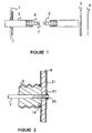
- the parabolic reflector antenna comprises a parabolic reflector 1 (fragmentarily illustrated), a feed tube 2 centrally mounted on the reflector 1, a dipole feed arrangement 3, in the form of a printed circuit board, located at the focal point of the parabolic reflector, and a solid metal sub-reflector 4, located approximately one quarter wavelength rearwardly of the dipole feed arrangement.
- Both the dipole arrangement 3 and the sub-reflector 4 are fixedly mounted by mounting means within an enclosing radome (not shown) attached to feed tube 2.
- a coaxial feeder cable 5, having an outer conductor 6 and an inner conductor 7 is located within the feed tube 2, and extends from the dipole feed arrangement to a terminal means, not shown, at rear of the reflector 1.
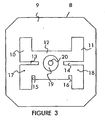
- the characteristic dipole feed arrangement 3 comprises an 8.0cm X 8.0cm octagonal shaped planar support 8 of insulating material, on one surface 9 ( Figure 3) of which is supported a conductive pattern comprising two parallel dipole elements 10 and 11, each being 3.5cm in length.
- the intermediate part of one dipole is connected to the intermediate part of the other dipole by a common conductor element 12.
- the conductor element includes two 13mm X 1mm collinear slots 13 and 14, each bifurcating an associated dipole. Each slot is approximately one quarter of an electrical wavelength at the operating frequency of the antenna (e.g. 3.5GHz). On one side of the conductor element 12, two spaced notches 15 and 16 are provided.
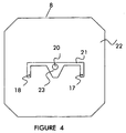
- the dipoles 10 and 11 are each provided with a through - connection 17, 18 which communicate with the opposite surface of planar support 8 (see Figure 4).
- the conductor element 12 also includes a circular area 19 which is free of conductive material. This area is coaxial with a central through-hole 20. The diameter of the circular area 19 is such that it is slightly smaller than the outside diameter of the outer conductor 6 of coaxial feeder cable 5. A rim of the conductive material bounding circular area 19 forms a first connection zone for connecting the conductor element 12, by, for example, soldering, to outer conductor 6 of the coaxial feeder 5, as shown in Figure 2.
- a conductive pattern in the form of a transmission line element 21, is supported on a surface 22 of the planar support.
- the transmission line element includes the above mentioned through-connections 17 and 18 which electrically connect the transmission line element to respective dipoles 10 and 11.
- Central through-hole 20, through planar support 8, permits the centre conductor 7 of the coaxial feeder 5 to be connected, by, for example, soldering, to a second connection zone 23, as shown in Figure 2.
- Optimum symmetry of the feed arrangement's radiation pattern requires that substantially identical current amplitudes flow in each half of each dipole. This can be achieved in the present invention by carefully selecting the location of each through-connection 17 and 18, and the location and depth of the notches 15 and 16.
- the dipole feed arrangement described above is implemented by using PCB techniques.
Landscapes
- Aerials With Secondary Devices (AREA)
- Variable-Direction Aerials And Aerial Arrays (AREA)
- Details Of Aerials (AREA)
Claims (8)
- Ensemble d'alimentation à dipôle (3) destiné à une antenne à réflecteur parabolique, ledit ensemble comprenant un élément planaire (8) en matériau isolant supportant, des deux côtés (9, 22) de celui-ci, un modèle de matériau conducteur, caractérisé en ce que,
sur un côté (9) dudit élément planaire (8), il possède un premier modèle de matériau conducteur formant au moins deux éléments de dipôles parallèles espacés (10, 11) de dimensions prédéterminées dont les parties intermédiaires respectives sont reliées par un seul élément conducteur (12) muni de deux encoches colinéaires opposées (13, 14) dont les longueurs électriques sont quasiment égales à un quart d'une longueur d'onde à la fréquence d'exploitation de ladite antenne, lesdites encoches (13, 14) bifurquant des dipôles respectifs (10, 11), ledit élément conducteur (12) comprenant une première zone de connexion (19) destinée à la connexion du conducteur externe (6) d'un câble d'alimentation coaxial (5), lesdites encoches et ledit élément conducteur faisant partie d'un moyen de symétriseur intégral, dans lequel ledit élément conducteur (12) comprend en outre au moins deux encoches espacées (15, 16) de profondeur prédéterminée et situées sur un côté dudit élément conducteur, et
dans lequel un second modèle de matériau conducteur est supporté sur l'autre côté (22) dudit élément planaire (8), formant un élément de ligne de transmission (21) muni d'une seconde zone de connexion (23) destinée à la connexion au conducteur interne (7) dudit câble d'alimentation coaxial (5), ladite première zone de connexion (19) et ladite seconde zone de connexion (23) étant sensiblement coaxiales, ledit élément de ligne de transmission (21) possédant deux moyens de connexion transversale espacés (17, 18) communiquant chacun avec une partie prédéterminée d'un élément de dipôle respectif. - Ensemble d'alimentation à dipôle (3) selon la revendication 1, dans lequel ledit premier modèle de matériau conducteur, ledit second modèle de matériau conducteur et ledit élément planaire (8) sont agencés sous la forme d'une carte de circuit imprimé.
- Ensemble d'antenne à réflecteur parabolique comprenant un élément de réflecteur parabolique (1), caractérisé en ce qu'il comprend un ensemble d'alimentation à dipôle (3) selon la revendication 1 ou 2 situé de manière fixe au niveau du point focal dudit élément de réflecteur parabolique (1), et un élément de sous-réflecteur (4) situé de manière fixe à une distance prédéterminée de l'ensemble d'alimentation à dipôle (3) éloigné dudit élément de réflecteur parabolique (1).
- Ensemble d'antenne à réflecteur parabolique selon la revendication 3, dans lequel ledit ensemble d'alimentation à dipôle (3) est placé de manière fixe par un tube (2) s'étendant de manière fixe à partir du centre dudit élément de réflecteur parabolique (1), ledit ensemble d'alimentation à dipôle (3) étant relié audit tube (2) au niveau du point focal de l'élément de réflecteur parabolique (1).
- Ensemble d'antenne à réflecteur parabolique selon la revendication 4, dans lequel un câble d'alimentation coaxial (5), comprenant un conducteur externe (6) et un conducteur interne (7), est situé dans ledit tube (2), ledit câble d'alimentation (5) s'étendant entre le moyen de terminal d'alimentation et les zones de connexion dudit ensemble d'alimentation à dipôle (3), ledit conducteur externe (6) étant électriquement relié à ladite première zone de connexion (19) et ledit conducteur interne (7) étant électriquement relié à ladite seconde zone de connexion (23).
- Ensemble d'antenne à réflecteur parabolique selon la revendication 5, dans lequel lesdits conducteurs interne (7) et externe (6) sont électriquement reliés aux zones de connexion respectives par soudure.
- Antenne à réflecteur parabolique selon l'une quelconque des revendications 3 à 6, dans laquelle ledit ensemble d'alimentation à dipôle (3) et ledit élément de sous-réflecteur (4) sont enfermés dans un capot d'antenne.
- Ensemble d'antenne à réflecteur parabolique selon la revendication 7, adapté pour fonctionner à une fréquence de 3,50 GHz.
Applications Claiming Priority (2)
| Application Number | Priority Date | Filing Date | Title |
|---|---|---|---|
| AUPP5495A AUPP549598A0 (en) | 1998-08-27 | 1998-08-27 | Dipole feed arrangement for a reflector antenna |
| AUPP549598 | 1998-08-27 |
Publications (3)
| Publication Number | Publication Date |
|---|---|
| EP0982802A2 EP0982802A2 (fr) | 2000-03-01 |
| EP0982802A3 EP0982802A3 (fr) | 2003-02-26 |
| EP0982802B1 true EP0982802B1 (fr) | 2005-09-07 |
Family
ID=3809722
Family Applications (1)
| Application Number | Title | Priority Date | Filing Date |
|---|---|---|---|
| EP99401951A Expired - Lifetime EP0982802B1 (fr) | 1998-08-27 | 1999-07-30 | Arrangement d'alimentation dipôle pour une antenne à réflecteur |
Country Status (6)
| Country | Link |
|---|---|
| US (1) | US6175338B1 (fr) |
| EP (1) | EP0982802B1 (fr) |
| AT (1) | ATE304227T1 (fr) |
| AU (1) | AUPP549598A0 (fr) |
| DE (1) | DE69927098T2 (fr) |
| ES (1) | ES2246561T3 (fr) |
Families Citing this family (8)
| Publication number | Priority date | Publication date | Assignee | Title |
|---|---|---|---|---|
| US6275181B1 (en) * | 1999-04-19 | 2001-08-14 | Advantest Corporation | Radio hologram observation apparatus and method therefor |
| JP3810265B2 (ja) * | 2000-09-19 | 2006-08-16 | インターナショナル・ビジネス・マシーンズ・コーポレーション | コンピュータシステム |
| US6674409B2 (en) * | 2000-12-05 | 2004-01-06 | Microtune (San Diego), Inc. | Balanced antenna structure for bluetooth 2.4 GHz physical region semiconductor integrated circuit |
| US6747605B2 (en) * | 2001-05-07 | 2004-06-08 | Atheros Communications, Inc. | Planar high-frequency antenna |
| US8228254B2 (en) * | 2001-06-14 | 2012-07-24 | Heinrich Foltz | Miniaturized antenna element and array |
| US6741219B2 (en) * | 2001-07-25 | 2004-05-25 | Atheros Communications, Inc. | Parallel-feed planar high-frequency antenna |
| JP2007194915A (ja) * | 2006-01-19 | 2007-08-02 | Sony Corp | アンテナ装置、アンテナ反射器、並びにアンテナを内蔵する無線通信機器 |
| TWM393816U (en) * | 2010-05-18 | 2010-12-01 | Hon Hai Prec Ind Co Ltd | Broadband antenna assembly |
Family Cites Families (2)
| Publication number | Priority date | Publication date | Assignee | Title |
|---|---|---|---|---|
| NO148579C (no) * | 1981-03-23 | 1983-11-02 | Sintef | Dipol-antenne |
| US5229782A (en) * | 1991-07-19 | 1993-07-20 | Conifer Corporation | Stacked dual dipole MMDS feed |
-
1998
- 1998-08-27 AU AUPP5495A patent/AUPP549598A0/en not_active Abandoned
-
1999
- 1999-06-03 US US09/324,854 patent/US6175338B1/en not_active Expired - Fee Related
- 1999-07-30 AT AT99401951T patent/ATE304227T1/de not_active IP Right Cessation
- 1999-07-30 EP EP99401951A patent/EP0982802B1/fr not_active Expired - Lifetime
- 1999-07-30 DE DE69927098T patent/DE69927098T2/de not_active Expired - Lifetime
- 1999-07-30 ES ES99401951T patent/ES2246561T3/es not_active Expired - Lifetime
Also Published As
| Publication number | Publication date |
|---|---|
| ATE304227T1 (de) | 2005-09-15 |
| ES2246561T3 (es) | 2006-02-16 |
| EP0982802A2 (fr) | 2000-03-01 |
| DE69927098D1 (de) | 2005-10-13 |
| AUPP549598A0 (en) | 1998-09-17 |
| EP0982802A3 (fr) | 2003-02-26 |
| US6175338B1 (en) | 2001-01-16 |
| DE69927098T2 (de) | 2006-01-26 |
Similar Documents
| Publication | Publication Date | Title |
|---|---|---|
| KR101056310B1 (ko) | 일체형 공급 구조체를 갖는 단일 또는 이중 분극 몰딩된 쌍극 안테나 | |
| US6650301B1 (en) | Single piece twin folded dipole antenna | |
| US6317099B1 (en) | Folded dipole antenna | |
| EP1376757B1 (fr) | Antenne directionnelle/omnidirectionnelle à double bande | |
| US5666126A (en) | Multi-staged antenna optimized for reception within multiple frequency bands | |
| US6809686B2 (en) | Multi-band antenna | |
| US6313798B1 (en) | Broadband microstrip antenna having a microstrip feedline trough formed in a radiating element | |
| US7151505B2 (en) | Quadrifilar helix antenna | |
| EP1098391B1 (fr) | Antenne doublet replié | |
| EP0132945B1 (fr) | Antenne | |
| KR20130090770A (ko) | 절연 특성을 가진 지향성 안테나 | |
| US6091366A (en) | Microstrip type antenna device | |
| US5777583A (en) | High gain broadband planar antenna | |
| US6483476B2 (en) | One-piece Yagi-Uda antenna and process for making the same | |
| EP0982802B1 (fr) | Arrangement d'alimentation dipôle pour une antenne à réflecteur | |
| IL300719A (en) | antenna array | |
| CN113745811A (zh) | 天线装置 | |
| US6014105A (en) | Microstrip antenna having an internal feed | |
| JPH1131915A (ja) | アンテナ及びアレイアンテナ | |
| AU764426B2 (en) | Dipole feed arrangement for a reflector antenna | |
| EP0826250B1 (fr) | Antenne a deux elements rayonnants a difference de phase reglable | |
| WO2023090212A1 (fr) | Dispositif d'antenne à demi-longueur d'onde et dispositif d'antenne à profil bas l'utilisant | |
| JP2005142925A (ja) | アンテナ装置 | |
| KR101992811B1 (ko) | 안테나 | |
| KR101992812B1 (ko) | 안테나 |
Legal Events
| Date | Code | Title | Description |
|---|---|---|---|
| PUAI | Public reference made under article 153(3) epc to a published international application that has entered the european phase |
Free format text: ORIGINAL CODE: 0009012 |
|
| AK | Designated contracting states |
Kind code of ref document: A2 Designated state(s): AT BE CH CY DE DK ES FI FR GB GR IE IT LI LU MC NL PT SE |
|
| AX | Request for extension of the european patent |
Free format text: AL;LT;LV;MK;RO;SI |
|
| PUAL | Search report despatched |
Free format text: ORIGINAL CODE: 0009013 |
|
| AK | Designated contracting states |
Kind code of ref document: A3 Designated state(s): AT BE CH CY DE DK ES FI FR GB GR IE IT LI LU MC NL PT SE Designated state(s): AT BE CH CY DE DK ES FI FR GB GR IE IT LI LU MC NL PT SE |
|
| AX | Request for extension of the european patent |
Extension state: AL LT LV MK RO SI |
|
| 17P | Request for examination filed |
Effective date: 20030303 |
|
| 17Q | First examination report despatched |
Effective date: 20030506 |
|
| AKX | Designation fees paid |
Designated state(s): AT BE CH CY DE DK ES FI FR GB GR IE IT LI LU MC NL PT SE |
|
| GRAP | Despatch of communication of intention to grant a patent |
Free format text: ORIGINAL CODE: EPIDOSNIGR1 |
|
| GRAS | Grant fee paid |
Free format text: ORIGINAL CODE: EPIDOSNIGR3 |
|
| GRAA | (expected) grant |
Free format text: ORIGINAL CODE: 0009210 |
|
| AK | Designated contracting states |
Kind code of ref document: B1 Designated state(s): AT BE CH CY DE DK ES FI FR GB GR IE IT LI LU MC NL PT SE |
|
| PG25 | Lapsed in a contracting state [announced via postgrant information from national office to epo] |
Ref country code: NL Free format text: LAPSE BECAUSE OF FAILURE TO SUBMIT A TRANSLATION OF THE DESCRIPTION OR TO PAY THE FEE WITHIN THE PRESCRIBED TIME-LIMIT Effective date: 20050907 Ref country code: LI Free format text: LAPSE BECAUSE OF FAILURE TO SUBMIT A TRANSLATION OF THE DESCRIPTION OR TO PAY THE FEE WITHIN THE PRESCRIBED TIME-LIMIT Effective date: 20050907 Ref country code: FI Free format text: LAPSE BECAUSE OF FAILURE TO SUBMIT A TRANSLATION OF THE DESCRIPTION OR TO PAY THE FEE WITHIN THE PRESCRIBED TIME-LIMIT Effective date: 20050907 Ref country code: CH Free format text: LAPSE BECAUSE OF FAILURE TO SUBMIT A TRANSLATION OF THE DESCRIPTION OR TO PAY THE FEE WITHIN THE PRESCRIBED TIME-LIMIT Effective date: 20050907 Ref country code: BE Free format text: LAPSE BECAUSE OF FAILURE TO SUBMIT A TRANSLATION OF THE DESCRIPTION OR TO PAY THE FEE WITHIN THE PRESCRIBED TIME-LIMIT Effective date: 20050907 Ref country code: AT Free format text: LAPSE BECAUSE OF FAILURE TO SUBMIT A TRANSLATION OF THE DESCRIPTION OR TO PAY THE FEE WITHIN THE PRESCRIBED TIME-LIMIT Effective date: 20050907 |
|
| REG | Reference to a national code |
Ref country code: GB Ref legal event code: FG4D |
|
| REG | Reference to a national code |
Ref country code: CH Ref legal event code: EP |
|
| REG | Reference to a national code |
Ref country code: IE Ref legal event code: FG4D |
|
| REF | Corresponds to: |
Ref document number: 69927098 Country of ref document: DE Date of ref document: 20051013 Kind code of ref document: P |
|
| PG25 | Lapsed in a contracting state [announced via postgrant information from national office to epo] |
Ref country code: SE Free format text: LAPSE BECAUSE OF FAILURE TO SUBMIT A TRANSLATION OF THE DESCRIPTION OR TO PAY THE FEE WITHIN THE PRESCRIBED TIME-LIMIT Effective date: 20051207 Ref country code: GR Free format text: LAPSE BECAUSE OF FAILURE TO SUBMIT A TRANSLATION OF THE DESCRIPTION OR TO PAY THE FEE WITHIN THE PRESCRIBED TIME-LIMIT Effective date: 20051207 Ref country code: DK Free format text: LAPSE BECAUSE OF FAILURE TO SUBMIT A TRANSLATION OF THE DESCRIPTION OR TO PAY THE FEE WITHIN THE PRESCRIBED TIME-LIMIT Effective date: 20051207 |
|
| PG25 | Lapsed in a contracting state [announced via postgrant information from national office to epo] |
Ref country code: PT Free format text: LAPSE BECAUSE OF FAILURE TO SUBMIT A TRANSLATION OF THE DESCRIPTION OR TO PAY THE FEE WITHIN THE PRESCRIBED TIME-LIMIT Effective date: 20060207 |
|
| REG | Reference to a national code |
Ref country code: ES Ref legal event code: FG2A Ref document number: 2246561 Country of ref document: ES Kind code of ref document: T3 |
|
| NLV1 | Nl: lapsed or annulled due to failure to fulfill the requirements of art. 29p and 29m of the patents act | ||
| REG | Reference to a national code |
Ref country code: CH Ref legal event code: PL |
|
| ET | Fr: translation filed | ||
| PLBE | No opposition filed within time limit |
Free format text: ORIGINAL CODE: 0009261 |
|
| STAA | Information on the status of an ep patent application or granted ep patent |
Free format text: STATUS: NO OPPOSITION FILED WITHIN TIME LIMIT |
|
| PG25 | Lapsed in a contracting state [announced via postgrant information from national office to epo] |
Ref country code: MC Free format text: LAPSE BECAUSE OF NON-PAYMENT OF DUE FEES Effective date: 20060731 Ref country code: IE Free format text: LAPSE BECAUSE OF NON-PAYMENT OF DUE FEES Effective date: 20060731 |
|
| 26N | No opposition filed |
Effective date: 20060608 |
|
| REG | Reference to a national code |
Ref country code: IE Ref legal event code: MM4A |
|
| PG25 | Lapsed in a contracting state [announced via postgrant information from national office to epo] |
Ref country code: LU Free format text: LAPSE BECAUSE OF NON-PAYMENT OF DUE FEES Effective date: 20060730 |
|
| PG25 | Lapsed in a contracting state [announced via postgrant information from national office to epo] |
Ref country code: CY Free format text: LAPSE BECAUSE OF FAILURE TO SUBMIT A TRANSLATION OF THE DESCRIPTION OR TO PAY THE FEE WITHIN THE PRESCRIBED TIME-LIMIT Effective date: 20050907 |
|
| PGFP | Annual fee paid to national office [announced via postgrant information from national office to epo] |
Ref country code: ES Payment date: 20100726 Year of fee payment: 12 |
|
| PGFP | Annual fee paid to national office [announced via postgrant information from national office to epo] |
Ref country code: IT Payment date: 20100727 Year of fee payment: 12 |
|
| PG25 | Lapsed in a contracting state [announced via postgrant information from national office to epo] |
Ref country code: IT Free format text: LAPSE BECAUSE OF NON-PAYMENT OF DUE FEES Effective date: 20110730 |
|
| REG | Reference to a national code |
Ref country code: ES Ref legal event code: FD2A Effective date: 20130606 |
|
| PG25 | Lapsed in a contracting state [announced via postgrant information from national office to epo] |
Ref country code: ES Free format text: LAPSE BECAUSE OF NON-PAYMENT OF DUE FEES Effective date: 20110731 |
|
| REG | Reference to a national code |
Ref country code: FR Ref legal event code: GC Effective date: 20140717 |
|
| REG | Reference to a national code |
Ref country code: FR Ref legal event code: RG Effective date: 20141016 |
|
| REG | Reference to a national code |
Ref country code: FR Ref legal event code: PLFP Year of fee payment: 17 |
|
| REG | Reference to a national code |
Ref country code: FR Ref legal event code: PLFP Year of fee payment: 18 |
|
| PGFP | Annual fee paid to national office [announced via postgrant information from national office to epo] |
Ref country code: DE Payment date: 20160722 Year of fee payment: 18 Ref country code: GB Payment date: 20160721 Year of fee payment: 18 |
|
| PGFP | Annual fee paid to national office [announced via postgrant information from national office to epo] |
Ref country code: FR Payment date: 20160721 Year of fee payment: 18 |
|
| REG | Reference to a national code |
Ref country code: DE Ref legal event code: R119 Ref document number: 69927098 Country of ref document: DE |
|
| GBPC | Gb: european patent ceased through non-payment of renewal fee |
Effective date: 20170730 |
|
| REG | Reference to a national code |
Ref country code: FR Ref legal event code: ST Effective date: 20180330 |
|
| PG25 | Lapsed in a contracting state [announced via postgrant information from national office to epo] |
Ref country code: DE Free format text: LAPSE BECAUSE OF NON-PAYMENT OF DUE FEES Effective date: 20180201 Ref country code: GB Free format text: LAPSE BECAUSE OF NON-PAYMENT OF DUE FEES Effective date: 20170730 |
|
| PG25 | Lapsed in a contracting state [announced via postgrant information from national office to epo] |
Ref country code: FR Free format text: LAPSE BECAUSE OF NON-PAYMENT OF DUE FEES Effective date: 20170731 |
|
| REG | Reference to a national code |
Ref country code: DE Ref legal event code: R082 Ref document number: 69927098 Country of ref document: DE Representative=s name: BARKHOFF REIMANN VOSSIUS, DE Ref country code: DE Ref legal event code: R081 Ref document number: 69927098 Country of ref document: DE Owner name: WSOU INVESTMENTS, LLC, LOS ANGELES, US Free format text: FORMER OWNER: ALCATEL LUCENT, PARIS, FR |
|
| REG | Reference to a national code |
Ref country code: GB Ref legal event code: 732E Free format text: REGISTERED BETWEEN 20200820 AND 20200826 |