EP0976007B1 - Optischer modulator - Google Patents
Optischer modulator Download PDFInfo
- Publication number
- EP0976007B1 EP0976007B1 EP98914986A EP98914986A EP0976007B1 EP 0976007 B1 EP0976007 B1 EP 0976007B1 EP 98914986 A EP98914986 A EP 98914986A EP 98914986 A EP98914986 A EP 98914986A EP 0976007 B1 EP0976007 B1 EP 0976007B1
- Authority
- EP
- European Patent Office
- Prior art keywords
- optical
- waveguide
- fibre
- output
- modulator according
- Prior art date
- Legal status (The legal status is an assumption and is not a legal conclusion. Google has not performed a legal analysis and makes no representation as to the accuracy of the status listed.)
- Expired - Lifetime
Links
Images
Classifications
-
- G—PHYSICS
- G02—OPTICS
- G02F—OPTICAL DEVICES OR ARRANGEMENTS FOR THE CONTROL OF LIGHT BY MODIFICATION OF THE OPTICAL PROPERTIES OF THE MEDIA OF THE ELEMENTS INVOLVED THEREIN; NON-LINEAR OPTICS; FREQUENCY-CHANGING OF LIGHT; OPTICAL LOGIC ELEMENTS; OPTICAL ANALOGUE/DIGITAL CONVERTERS
- G02F1/00—Devices or arrangements for the control of the intensity, colour, phase, polarisation or direction of light arriving from an independent light source, e.g. switching, gating or modulating; Non-linear optics
- G02F1/01—Devices or arrangements for the control of the intensity, colour, phase, polarisation or direction of light arriving from an independent light source, e.g. switching, gating or modulating; Non-linear optics for the control of the intensity, phase, polarisation or colour
- G02F1/011—Devices or arrangements for the control of the intensity, colour, phase, polarisation or direction of light arriving from an independent light source, e.g. switching, gating or modulating; Non-linear optics for the control of the intensity, phase, polarisation or colour in optical waveguides, not otherwise provided for in this subclass
- G02F1/0115—Devices or arrangements for the control of the intensity, colour, phase, polarisation or direction of light arriving from an independent light source, e.g. switching, gating or modulating; Non-linear optics for the control of the intensity, phase, polarisation or colour in optical waveguides, not otherwise provided for in this subclass in optical fibres
-
- G—PHYSICS
- G02—OPTICS
- G02F—OPTICAL DEVICES OR ARRANGEMENTS FOR THE CONTROL OF LIGHT BY MODIFICATION OF THE OPTICAL PROPERTIES OF THE MEDIA OF THE ELEMENTS INVOLVED THEREIN; NON-LINEAR OPTICS; FREQUENCY-CHANGING OF LIGHT; OPTICAL LOGIC ELEMENTS; OPTICAL ANALOGUE/DIGITAL CONVERTERS
- G02F1/00—Devices or arrangements for the control of the intensity, colour, phase, polarisation or direction of light arriving from an independent light source, e.g. switching, gating or modulating; Non-linear optics
- G02F1/01—Devices or arrangements for the control of the intensity, colour, phase, polarisation or direction of light arriving from an independent light source, e.g. switching, gating or modulating; Non-linear optics for the control of the intensity, phase, polarisation or colour
- G02F1/011—Devices or arrangements for the control of the intensity, colour, phase, polarisation or direction of light arriving from an independent light source, e.g. switching, gating or modulating; Non-linear optics for the control of the intensity, phase, polarisation or colour in optical waveguides, not otherwise provided for in this subclass
-
- G—PHYSICS
- G02—OPTICS
- G02F—OPTICAL DEVICES OR ARRANGEMENTS FOR THE CONTROL OF LIGHT BY MODIFICATION OF THE OPTICAL PROPERTIES OF THE MEDIA OF THE ELEMENTS INVOLVED THEREIN; NON-LINEAR OPTICS; FREQUENCY-CHANGING OF LIGHT; OPTICAL LOGIC ELEMENTS; OPTICAL ANALOGUE/DIGITAL CONVERTERS
- G02F1/00—Devices or arrangements for the control of the intensity, colour, phase, polarisation or direction of light arriving from an independent light source, e.g. switching, gating or modulating; Non-linear optics
- G02F1/01—Devices or arrangements for the control of the intensity, colour, phase, polarisation or direction of light arriving from an independent light source, e.g. switching, gating or modulating; Non-linear optics for the control of the intensity, phase, polarisation or colour
- G02F1/011—Devices or arrangements for the control of the intensity, colour, phase, polarisation or direction of light arriving from an independent light source, e.g. switching, gating or modulating; Non-linear optics for the control of the intensity, phase, polarisation or colour in optical waveguides, not otherwise provided for in this subclass
- G02F1/0113—Glass-based, e.g. silica-based, optical waveguides
-
- G—PHYSICS
- G02—OPTICS
- G02F—OPTICAL DEVICES OR ARRANGEMENTS FOR THE CONTROL OF LIGHT BY MODIFICATION OF THE OPTICAL PROPERTIES OF THE MEDIA OF THE ELEMENTS INVOLVED THEREIN; NON-LINEAR OPTICS; FREQUENCY-CHANGING OF LIGHT; OPTICAL LOGIC ELEMENTS; OPTICAL ANALOGUE/DIGITAL CONVERTERS
- G02F1/00—Devices or arrangements for the control of the intensity, colour, phase, polarisation or direction of light arriving from an independent light source, e.g. switching, gating or modulating; Non-linear optics
- G02F1/01—Devices or arrangements for the control of the intensity, colour, phase, polarisation or direction of light arriving from an independent light source, e.g. switching, gating or modulating; Non-linear optics for the control of the intensity, phase, polarisation or colour
- G02F1/0126—Opto-optical modulation, i.e. control of one light beam by another light beam, not otherwise provided for in this subclass
-
- G—PHYSICS
- G02—OPTICS
- G02F—OPTICAL DEVICES OR ARRANGEMENTS FOR THE CONTROL OF LIGHT BY MODIFICATION OF THE OPTICAL PROPERTIES OF THE MEDIA OF THE ELEMENTS INVOLVED THEREIN; NON-LINEAR OPTICS; FREQUENCY-CHANGING OF LIGHT; OPTICAL LOGIC ELEMENTS; OPTICAL ANALOGUE/DIGITAL CONVERTERS
- G02F1/00—Devices or arrangements for the control of the intensity, colour, phase, polarisation or direction of light arriving from an independent light source, e.g. switching, gating or modulating; Non-linear optics
- G02F1/01—Devices or arrangements for the control of the intensity, colour, phase, polarisation or direction of light arriving from an independent light source, e.g. switching, gating or modulating; Non-linear optics for the control of the intensity, phase, polarisation or colour
- G02F1/015—Devices or arrangements for the control of the intensity, colour, phase, polarisation or direction of light arriving from an independent light source, e.g. switching, gating or modulating; Non-linear optics for the control of the intensity, phase, polarisation or colour based on semiconductor elements having potential barriers, e.g. having a PN or PIN junction
- G02F1/0151—Devices or arrangements for the control of the intensity, colour, phase, polarisation or direction of light arriving from an independent light source, e.g. switching, gating or modulating; Non-linear optics for the control of the intensity, phase, polarisation or colour based on semiconductor elements having potential barriers, e.g. having a PN or PIN junction modulating the refractive index
- G02F1/0153—Devices or arrangements for the control of the intensity, colour, phase, polarisation or direction of light arriving from an independent light source, e.g. switching, gating or modulating; Non-linear optics for the control of the intensity, phase, polarisation or colour based on semiconductor elements having potential barriers, e.g. having a PN or PIN junction modulating the refractive index using electro-refraction, e.g. Kramers-Kronig relation
-
- G—PHYSICS
- G02—OPTICS
- G02F—OPTICAL DEVICES OR ARRANGEMENTS FOR THE CONTROL OF LIGHT BY MODIFICATION OF THE OPTICAL PROPERTIES OF THE MEDIA OF THE ELEMENTS INVOLVED THEREIN; NON-LINEAR OPTICS; FREQUENCY-CHANGING OF LIGHT; OPTICAL LOGIC ELEMENTS; OPTICAL ANALOGUE/DIGITAL CONVERTERS
- G02F1/00—Devices or arrangements for the control of the intensity, colour, phase, polarisation or direction of light arriving from an independent light source, e.g. switching, gating or modulating; Non-linear optics
- G02F1/01—Devices or arrangements for the control of the intensity, colour, phase, polarisation or direction of light arriving from an independent light source, e.g. switching, gating or modulating; Non-linear optics for the control of the intensity, phase, polarisation or colour
- G02F1/03—Devices or arrangements for the control of the intensity, colour, phase, polarisation or direction of light arriving from an independent light source, e.g. switching, gating or modulating; Non-linear optics for the control of the intensity, phase, polarisation or colour based on ceramics or electro-optical crystals, e.g. exhibiting Pockels effect or Kerr effect
- G02F1/035—Devices or arrangements for the control of the intensity, colour, phase, polarisation or direction of light arriving from an independent light source, e.g. switching, gating or modulating; Non-linear optics for the control of the intensity, phase, polarisation or colour based on ceramics or electro-optical crystals, e.g. exhibiting Pockels effect or Kerr effect in an optical waveguide structure
Definitions
- This invention relates to an optical modulator for use in waveguides such as optical fibres or planar substrate devices.
- an optical multi-waveguide interference filter in which a first waveguide capable of single mode transmission, is coupled to a second waveguide capable of supporting at least two transmission modes.
- a third waveguide supporting a single mode is used to pick up light from the second, multimode waveguide.
- light in a single mode passes from the first waveguide into the second waveguide where it is transmitted in two modes, which interfere with one another.
- the interfering modes produce an amplitude peak at the entrance to the third waveguide, which shifts diametrically across the input to the third waveguide as a function of wavelength.
- the filter is described in detail in "An Optical Multi-waveguide Interference Filter” M. Earnshaw et al, Optics Communications 116 (1995), 339-342, 1 May 1995.
- Electro-optic modulation of a silica-based fibre has been proposed by T. Fujiwara et al, Electronics Letters, 30 March 1995, Vol. 31 No. 7, pp 573-575.
- a voltage was applied to wires inserted into the fibre whilst irradiating it with ultraviolet radiation. Thereafter, the application of a voltage to the wires produced a phase shift for optical radiation transmitted through the fibre.
- the present invention provides a new approach for producing modulation in an optical waveguide.
- the waveguide may be formed of electrically poled material, which may be thermally poled.
- the modulator according to the invention may be formed in an optical fibre, such as silica-based fibre, which has been thermally poled.
- the fibre may include electrode means running along the length thereof to permit a modulating voltage to be applied.
- a modulator according to the invention may also be embodied in a planar waveguide device.
- the invention also includes a method of modulating optical radiation according to claim 14.
- the modulation in accordance with the invention may be carried out with an optical waveguide comprising a plural mode region capable of supporting plural transmission modes with an electric field responsive refractive index, an electrode for applying an electric modulating field to the plural mode region and an output from the plural mode region to provide an optical output as a function of the applied modulating field.
- the optical waveguide may comprise a dual mode region having an electrically poled core, an output for single mode radiation and an electrode for applying an electric modulating field to the poled core.
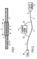
- an optical fibre arrangement including a modulator according to the invention is shown.
- the arrangement comprises a first, single mode fibre 1, a second, dual mode fibre 2 and a third length of fibre 3, which operates in single mode.
- the fibres 1 and 3 are fusion butt-jointed to opposite ends of the fibre 2, by means of fusion splices 4, 5.
- the fibres 1, 3 are conventional single mode fibres as used for optical telecommunications. They typically comprise silica based fibres with a Ge/B doped core 6, surrounded by a SiO 2 cladding 7. Typically, the core diameter is 8 ⁇ m and the exterior cladding diameter is 125 ⁇ m.
- the second fibre 2 includes a core 8 surrounded by a cladding 9 and is of the same general construction as the single mode fibres 1 and 3 but is capable of supporting multiple transmission modes.
- the core 8 of the multimode fibre 2 has a radius a that is less than that of the single mode fibres 1, 3, as will be described in more detail later, together with an appropriate value of ⁇ n, higher than that of the single mode fibres 1, 3, in order to satisfy the conditions required to support dual mode transmission.
- the fibre 2 may be formed of germania doped silica, with or without boron sodium or defect rich dopant such as cerium.
- the fibre in this example supports the LP 01 and LP 11 transmission modes.
- a typical length L for the fibre 2 is 2.4 cm.
- the length of the fibres 1, 3 is not critical
- Figure 2 illustrates a transverse cross section of the fibre 2 and generally corresponds to the optical fibre shown in Figure 9 of our copending WO-A-97/28481 (PCT/GB97/00266) filed on 30 January 1997.
- the fibre has a relatively broad dimension b and a relatively narrow dimension w in a second direction normal to the first direction.
- Two recesses 13, 14 having a depth d extend from planar surface regions 15, 16 towards the core 8 along the length of the fibre.
- the planar surface regions 15, 16 are connected by curved, cylindrical surface regions 17, 18 that extend along the length of the fibre.
- the breadth b is 250 ⁇ m
- the width w is 100 ⁇ m
- the depth of the recesses is of the order 30 ⁇ m.
- the bottom of the recesses 13, 14 are spaced from the core by 9-15 ⁇ m.
- the diameter of the core 8 is typically 4 - 8 ⁇ m and in this example is 6 ⁇ m.
- the value of ⁇ n for the fibre 2 is 0.012 and n cladding is 1.45
- the recesses are coated with electrodes 19, 20, formed by evaporation of a metallic source and deposition of the vapour in the recesses.
- the electrodes 19, 20 may be formed of gold.
- the recesses thereafter are filled with an electrically insulating material such as silicon rubber 21 so as to protect the fibre from glass/air dielectric breakdown and flash-over.
- external leads 22, 23 are connected to the electrodes 19, 20 respectively. Further details of the fibre structure, including details of its manufacture and the dopant concentrations used, are given in WO-A-97/28481 (PCT/GB97/00266).
- the core of fibre 2 is photosensitive to UV light. When doped with Ge or Ge and B, it is photosensitive to radiation with a wavelength of 244 nm.
- the material of the fibre can be poled by heating the fibre and applying an electric field between the electrodes 19, 20, whilst directing UV light at 244 nm towards the fibre. This is described in more detail in T. Fujiwara, D. Wong, Y. Zhao, S. Flemming v. Grishina and S. Poole "UV Excited Poling and Electrically Tunable Bragg Gratings in a Germo Silicate Fibre", post deadline paper OFC 1995 (Feb 1995).
- the poling voltage was applied directly to the electrodes 19, 20 and was up to 2kv over 35 ⁇ m, giving a field strength of the order of 5 - 6 x10 7 v/m.
- the poling voltage may be applied to the fibre using an additional electrode on a Si wafer as described in "A Poled Electrooptic Fiber” X.C. Long et al, IEEE Photonics Technology Lett. Vol 8, No 2, February 1996, pp 227-229.
- the poling temperature was 260-280°C.
- the fibre presents a different refractive index to the LP 01 and the LP 11 transmission mode resulting in a voltage-dependent phase difference between them.
- the two modes interfere by an amount dependent upon the applied voltage.
- the amplitude peak produced as a result of interference can be swept across the entrance to the single mode core of the third fibre 3 shown in Figure 1, at the butt joint 5.
- the intensity of light received at the optical detector 12 can be varied.
- the device can be used as a modulator.
- a specific example of the applied voltage range is up to 1 kv. This corresponds to a range of applied field of 0 ⁇ 10 7 v/m.
- the contrast ratio achievable is of the order of 100%.
- the bit rate that can be achieved by means of the described example optical modulator according to the invention is of the order of ten times greater than can be achieved with a comparable conventional lithium niobate doped optical fibre modulator and is typically > 20GHz.
- the optical waveguide is formed in a planar substrate, typically made of silicon. Details of how a silicon substrate can be processed in order to provide a doped silica waveguide as an elongate strip, surrounded by an undoped silica cladding region, is discussed in detail in our US Patent No. 5 342 478 dated 30 August 1994.
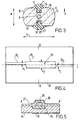
- the device comprises a silicon substrate 24 and an elongate waveguide 25 formed on the substrate 24.
- the substrate 24 is formed with a trench filled with thermal oxide 26 onto which a doped oxide layer is formed in order to form the core of the waveguide.
- the oxide layer (not shown) is plasma etched, using conventional lithographic techniques in order to form the pattern 25 shown in plan view in Figure 4. Thereafter, the region 25 is covered with an undoped oxide layer 27.
- the oxide layers 26 and 27 thus form a cladding around the core region 25 of the waveguide.
- the process may utilise the well known technique of local oxidisation of silicon (LOCOS), which is summarised in our previously mentioned US Patent No. 5 342 578.
- LOCS local oxidisation of silicon
- the waveguide core 25 includes a first region 25 1 capable of single mode operation, the second region 25 2 , wider than the first region, capable of supporting bi-moded transmission, and a third region 25 3 capable of single mode operation.
- Typical transverse dimensions x 1 , x 2 , x 3 for the regions 25 1 , 2 , 3 are 5 ⁇ m, 10 ⁇ m and 5 ⁇ m respectively.
- a typical thickness for the region 25 is of the order of 6 ⁇ m.
- the bi-moded region 25 2 is thus wider than the single moded regions 25 1 , 3 in contrast to the previously described fibre configuration of Figure 1.
- the value of the refractive index difference ⁇ n between the core and the cladding is the same for the bi-moded and single moded regions in order to simplify construction of the planar device, and so in order to satisfy the condition of equation (1) for bi-moded operation, the core dimension x 2 (corresponding to 2 a in equation (1)) is made greater than the dimensions x 1 , x 3 .
- a typical value for ⁇ n is 5 x 10 -3 and a typical approximate value of n cladding is 1,450.
- An example of the core dopant used is germania to a concentration of approximately 3 mole percent.
- the single moded regions 25 1 , 25 3 are offset from the longitudinal centreline y of the core 25, in the manner described by Earnshaw et al, supra .
- the electrodes 28, 29 can thus be used to pole the core region 25 2 by thermal poling and/or by UV radiation, in the manner previously explained.
- the electrodes 28, 29 are connected to ohmic contact pads (not shown) for connection to the leads 22, 23, shown in Figure 2 so that a modulating voltage can be applied from the source V.
- the temperature, field strengths and voltages used for poling and modulation are substantially the same as for the embodiment of Figure 1.
- light from the laser 10 is directed into the first, single mode portion of the core 25 1 from which it passes into the bi-modal region 25 2 .
- the two modes of propagation interfere with one another, in the manner previously described.
- the phase difference between the interfering modes depends on the voltage V applied to the electrodes 26, 27 in the bi-modal region 25 2 and the interference peak which can be produced at the entrance to the third single mode region 25 3 is shifted laterally across the width of the entrance depending on the applied voltage.
- the intensity of the light entering the single mode region 25 3 depends on the applied voltage.
- the device can be used to modulate the light output that is fed to the optical detector 12.
- optical radiation includes both visible and non-visible optical radiation, such as ultraviolet and infrared.
Landscapes
- Physics & Mathematics (AREA)
- Nonlinear Science (AREA)
- General Physics & Mathematics (AREA)
- Optics & Photonics (AREA)
- Optical Modulation, Optical Deflection, Nonlinear Optics, Optical Demodulation, Optical Logic Elements (AREA)
- Optical Integrated Circuits (AREA)
- Light Guides In General And Applications Therefor (AREA)
- Electrochromic Elements, Electrophoresis, Or Variable Reflection Or Absorption Elements (AREA)
Claims (14)
- Optischer Modulator mit
einem Wellenleiter (2), der erste und zweite verschiedene optische Übertragungsmoden bei einer gegebenen Wellenlänge unterstützt, einem Eingang zum Eingeben von optischer Strahlung in den Wellenleiter,
einem Ausgang zum Übertragen von optischer Strahlung aus dem Wellenleiter, wobei die Intensität der Strahlung, die durch den Ausgang tritt, eine Funktion der relativen Phasen der ersten und der zweiten Moden am Ausgang ist,
einer Modulationseinrichtung (v), um die Phasendifferenz zwischen den Moden am Ausgang zu ändern und dadurch die Intensität der optischen Strahlung zu steuern, die durch den Ausgang tritt, und
ersten und zweiten optischen Fasern (1, 3), die an den Eingang beziehungsweise den Ausgang gekoppelt sind, wobei die optischen Fasern eine optische Übertragung im Einmodenbetrieb bei der vorgegebenen Wellenlänge unterstützen,
dadurch gekennzeichnet, dass die Modulationseinrichtung eingerichtet ist, um ein elektrisches Feld an den Wellenleiter (2) anzulegen, um die Phasendifferenz zu bewirken. - Optischer Modulator nach Anspruch 1, bei dem der Wellenleiter (2) aus elektrooptischem Material besteht und die Modulationseinrichtung (v) eine Einrichtung zum Anlegen des elektrischen Feldes an das Material umfasst.
- Optischer Modulator nach Anspruch 2, der eine Elektrode (19, 20) zum Anlegen des elektrischen Feldes an den Wellenleiter umfasst.
- Optischer Modulator nach Anspruch 3, bei dem die Elektrode (19, 20) auf dem Wellenleiter (2) angebracht ist.
- Optischer Modulator nach Anspruch 4, bei dem die Elektrode (19, 20) in einer längs verlaufenden Vertiefung (13, 14) in dem Wellenleiter vorgesehen ist.
- Optischer Modulator nach Anspruch 2, 3, 4 oder 5, bei dem das elektrooptische Material elektrisch polares Material enthält.
- Optischer Modulator nach Anspruch 6, bei dem das elektrisch polare Material thermisch polarisiert ist.
- Optischer Modulator nach Anspruch 7, bei dem das elektrisch polare Material thermisch polarisierten Quarz enthält.
- Optischer Modulator nach einem der vorangehenden Ansprüche, bei dem der Wellenleiter (2) eine optische Faser umfasst.
- Optischer Modulator nach Anspruch 9, bei dem die Faser dazu eingerichtet ist, zwei Übertragungsmoden zu unterstützen.
- Optischer Modulator nach einem der Ansprüche 1 bis 8, bei dem der Wellenleiter (2) eine planare Struktur auf einem Substrat umfasst.
- Optischer Modulator nach einem der vorangehenden Ansprüche, bei dem der Wellenleiter (2) mit ultravioletter Strahlung polarisiert wurde.
- Verwendung eines optischen Modulators nach Anspruch 1, um ein optisches Signal bei einer gegebenen Wellenlänge zu modulieren, das von der ersten optischen Einmodenfaser, die an den Eingang des Modulators angeschlossen ist, zu der zweiten Einmodenfaser läuft, die an den Ausgang des Modulators angeschlossen ist.
- Verfahren zur Modulation von optischer Strahlung, wobei das Verfahren folgendes umfasst:Einkoppeln der optischen Strahlung mit einer vorgegebenen Wellenlänge von einer ersten optischen Einmodenfaser in einen optischen Wellenleiter, der erste und zweite verschiedene optische Übertragungsmoden bei der vorgegebenen Wellenlänge unterstützt, und der einen Ausgang hat, an den eine zweite optische Faser gekoppelt ist, die bei der gegebenen Wellenlänge im Einmodenbetrieb arbeitet, wobei die optische Intensität der Strahlung am Ausgang des Wellenleiters eine Funktion der relativen Phasen der ersten und der zweiten Moden am Ausgang ist, undAnlegen eines externen elektrischen Feldes an den Wellenleiter, um die Phasendifferenz zwischen den Moden am Ausgang zu verändern, und dadurch die Intensität der optischen Strahlung, die in die zweite optische Faser eingekoppelt wird, zu modulieren.
Priority Applications (1)
| Application Number | Priority Date | Filing Date | Title |
|---|---|---|---|
| EP98914986A EP0976007B1 (de) | 1997-04-14 | 1998-04-06 | Optischer modulator |
Applications Claiming Priority (4)
| Application Number | Priority Date | Filing Date | Title |
|---|---|---|---|
| EP97302524A EP0872756A1 (de) | 1997-04-14 | 1997-04-14 | Optischer Modulator |
| EP97302524 | 1997-04-14 | ||
| EP98914986A EP0976007B1 (de) | 1997-04-14 | 1998-04-06 | Optischer modulator |
| PCT/GB1998/001010 WO1998047041A1 (en) | 1997-04-14 | 1998-04-06 | Optical modulator |
Publications (2)
| Publication Number | Publication Date |
|---|---|
| EP0976007A1 EP0976007A1 (de) | 2000-02-02 |
| EP0976007B1 true EP0976007B1 (de) | 2004-02-04 |
Family
ID=8229292
Family Applications (2)
| Application Number | Title | Priority Date | Filing Date |
|---|---|---|---|
| EP97302524A Withdrawn EP0872756A1 (de) | 1997-04-14 | 1997-04-14 | Optischer Modulator |
| EP98914986A Expired - Lifetime EP0976007B1 (de) | 1997-04-14 | 1998-04-06 | Optischer modulator |
Family Applications Before (1)
| Application Number | Title | Priority Date | Filing Date |
|---|---|---|---|
| EP97302524A Withdrawn EP0872756A1 (de) | 1997-04-14 | 1997-04-14 | Optischer Modulator |
Country Status (6)
| Country | Link |
|---|---|
| US (1) | US6094291A (de) |
| EP (2) | EP0872756A1 (de) |
| AU (1) | AU6928098A (de) |
| CA (1) | CA2286049C (de) |
| DE (1) | DE69821476T2 (de) |
| WO (1) | WO1998047041A1 (de) |
Families Citing this family (19)
| Publication number | Priority date | Publication date | Assignee | Title |
|---|---|---|---|---|
| US6563589B1 (en) | 1996-04-19 | 2003-05-13 | Kvh Industries, Inc. | Reduced minimum configuration fiber optic current sensor |
| JPH1090546A (ja) * | 1996-09-17 | 1998-04-10 | Toyota Motor Corp | 平面導波路の製造方法及び平面導波路 |
| US6891622B2 (en) | 1999-02-11 | 2005-05-10 | Kvh Industries, Inc. | Current sensor |
| US6539134B1 (en) | 1999-02-11 | 2003-03-25 | Kvh Industries, Inc. | Polarization transformer |
| US6424755B1 (en) * | 1999-07-02 | 2002-07-23 | Nortel Networks Limited | Slotted monolithic optical waveguides |
| US6476951B1 (en) * | 1999-09-14 | 2002-11-05 | Fitel Usa Corp. | Use of mode coupled optical fiber in communications systems |
| US6259830B1 (en) | 1999-11-30 | 2001-07-10 | Corning, Incorporated | Poled electro-optic device and method |
| US6370289B1 (en) | 2000-01-12 | 2002-04-09 | Kvh Industries, Inc. | Apparatus and method for electronic RIN reduction in fiber-optic sensors |
| US6703821B2 (en) | 2000-02-28 | 2004-03-09 | Kvh Industries, Inc. | Faraday-effect current sensor with improved vibration response |
| US6594020B2 (en) | 2000-07-13 | 2003-07-15 | Kvh Industries, Inc | Method for controlling fiber optic sensor scale factor using amplitude modulation |
| US6718097B2 (en) | 2000-07-18 | 2004-04-06 | Kvh Industries, Inc. | Method of incorporating optical material into an optical fiber |
| WO2002010813A2 (en) | 2000-08-02 | 2002-02-07 | Kvh Industries, Inc. | Reduction of linear birefringence in circular-core single-mode fiber |
| US6707558B2 (en) | 2000-08-02 | 2004-03-16 | Kvh Industries, Inc. | Decreasing the effects of linear birefringence in a fiber-optic sensor by use of Berry's topological phase |
| CN1474952A (zh) * | 2000-09-26 | 2004-02-11 | ��ķ�ɷ�����˾ | 光波导和序列波导光栅中的双折射控制 |
| US6880275B2 (en) * | 2001-05-16 | 2005-04-19 | Hon Technology Inc. | Lenticular fireplace |
| US6836334B2 (en) | 2001-10-31 | 2004-12-28 | Kvh Industries, Inc. | Angle random walk (ARW) noise reduction in fiber optic sensors using an optical amplifier |
| KR100420951B1 (ko) * | 2002-04-17 | 2004-03-02 | 한국전자통신연구원 | 분극 광섬유, 분극 광섬유를 제조하는 방법 및 분산 보상기 |
| US6763153B2 (en) | 2002-04-17 | 2004-07-13 | Kvh Industries, Inc. | Apparatus and method for electronic RIN reduction in fiber-optic sensors utilizing filter with group delay |
| EP1426794B1 (de) * | 2002-12-03 | 2005-10-12 | Alcatel | Dünnschichtfilter auf der Endfläche eines Glasfasersegments, Herstellungsverfahren und integrierte optische Vorrichtung |
Family Cites Families (7)
| Publication number | Priority date | Publication date | Assignee | Title |
|---|---|---|---|---|
| US4791388A (en) * | 1987-04-27 | 1988-12-13 | Polaroid Corporation | Channel waveguide modulator |
| US5082349A (en) * | 1988-04-25 | 1992-01-21 | The Board Of Trustees Of The Leland Stanford Junior University | Bi-domain two-mode single crystal fiber devices |
| US5247601A (en) * | 1991-09-27 | 1993-09-21 | Myers Richard A | Arrangement for producing large second-order optical nonlinearities in a waveguide structure including amorphous SiO2 |
| US5239407A (en) * | 1991-09-27 | 1993-08-24 | University Of New Mexico | Method and apparatus for creating large second-order nonlinearities in fused silica |
| US5617499A (en) * | 1995-09-08 | 1997-04-01 | University Of New Mexico | Technique for fabrication of a poled electrooptic fiber segment |
| EP0877968B1 (de) * | 1996-01-30 | 2000-09-27 | BRITISH TELECOMMUNICATIONS public limited company | Optischer wellenleiter |
| US5867615A (en) * | 1997-07-22 | 1999-02-02 | The United States Of America As Represented By The Secretary Of The Air Force | Compact straight channel fiber optic intensity modular |
-
1997
- 1997-04-14 EP EP97302524A patent/EP0872756A1/de not_active Withdrawn
-
1998
- 1998-04-06 WO PCT/GB1998/001010 patent/WO1998047041A1/en not_active Ceased
- 1998-04-06 EP EP98914986A patent/EP0976007B1/de not_active Expired - Lifetime
- 1998-04-06 US US09/068,959 patent/US6094291A/en not_active Expired - Lifetime
- 1998-04-06 CA CA002286049A patent/CA2286049C/en not_active Expired - Fee Related
- 1998-04-06 AU AU69280/98A patent/AU6928098A/en not_active Abandoned
- 1998-04-06 DE DE69821476T patent/DE69821476T2/de not_active Expired - Fee Related
Also Published As
| Publication number | Publication date |
|---|---|
| DE69821476T2 (de) | 2004-11-25 |
| EP0872756A1 (de) | 1998-10-21 |
| CA2286049A1 (en) | 1998-10-22 |
| US6094291A (en) | 2000-07-25 |
| AU6928098A (en) | 1998-11-11 |
| WO1998047041A1 (en) | 1998-10-22 |
| CA2286049C (en) | 2007-06-26 |
| EP0976007A1 (de) | 2000-02-02 |
| DE69821476D1 (de) | 2004-03-11 |
Similar Documents
| Publication | Publication Date | Title |
|---|---|---|
| EP0976007B1 (de) | Optischer modulator | |
| Takato et al. | Silica-based single-mode waveguides on silicon and their application to guided-wave optical interferometers | |
| US8649639B2 (en) | Method and system for waveguide mode filters | |
| JP4562339B2 (ja) | 差動導波路対 | |
| USRE41748E1 (en) | Tunable bragg grating and devices employing the same | |
| US12265253B2 (en) | Low loss fiber-to-chip interfaces for lithium niobate photonic integrated circuits | |
| US6859567B2 (en) | In-guide control of optical propagation | |
| EP1055958A1 (de) | Aktives optisches multimodales Interferenzwellenleiterbauelement | |
| US5982961A (en) | Organic crystal compound optical waveguide and methods for its fabrication | |
| CA2295815A1 (en) | Fiber grating and fiber optic devices using the same | |
| WO1998040783A1 (en) | Hybrid digital electro-optic switch | |
| JP4448859B2 (ja) | 光デバイスにおける光ビームをフォトニック結晶格子により調整するための装置および方法 | |
| EP0877968B1 (de) | Optischer wellenleiter | |
| US6008927A (en) | Optical fiber modulator having an optical fiber having a poled portion serving as an electrooptic element and method for making same | |
| JP3573180B2 (ja) | マッハ・ツェンダ干渉計アームのポーリング方法 | |
| US5119450A (en) | Broad wavelength range single mode integrated optics device | |
| AU757486B2 (en) | Electrostrictive fiber modulators | |
| US20010030982A1 (en) | All-polymer waveguide polarization modulator and method of mode profile control and excitation | |
| US10768454B2 (en) | Athermal modulator-switch with two superimposed rings | |
| JPWO2004086126A1 (ja) | 導波路型光変調器 | |
| US6101297A (en) | Waveguide type polarization scrambler | |
| JP5443314B2 (ja) | 光変調器 | |
| JP3418391B2 (ja) | 導波型光デバイスの製造方法 | |
| JPH0980364A (ja) | 導波路型光デバイス | |
| Nakatsuhara et al. | Si-waveguide with ferro-electric liquid crystal cladding for use in optical switching devices |
Legal Events
| Date | Code | Title | Description |
|---|---|---|---|
| PUAI | Public reference made under article 153(3) epc to a published international application that has entered the european phase |
Free format text: ORIGINAL CODE: 0009012 |
|
| 17P | Request for examination filed |
Effective date: 19990920 |
|
| AK | Designated contracting states |
Kind code of ref document: A1 Designated state(s): DE FR GB IT |
|
| RBV | Designated contracting states (corrected) |
Designated state(s): DE FR GB IT |
|
| 17Q | First examination report despatched |
Effective date: 20011018 |
|
| PGFP | Annual fee paid to national office [announced via postgrant information from national office to epo] |
Ref country code: FR Payment date: 20030311 Year of fee payment: 7 |
|
| GRAP | Despatch of communication of intention to grant a patent |
Free format text: ORIGINAL CODE: EPIDOSNIGR1 |
|
| GRAS | Grant fee paid |
Free format text: ORIGINAL CODE: EPIDOSNIGR3 |
|
| GRAA | (expected) grant |
Free format text: ORIGINAL CODE: 0009210 |
|
| AK | Designated contracting states |
Kind code of ref document: B1 Designated state(s): DE FR GB IT |
|
| PG25 | Lapsed in a contracting state [announced via postgrant information from national office to epo] |
Ref country code: IT Free format text: LAPSE BECAUSE OF FAILURE TO SUBMIT A TRANSLATION OF THE DESCRIPTION OR TO PAY THE FEE WITHIN THE PRE;WARNING: LAPSES OF ITALIAN PATENTS WITH EFFECTIVE DATE BEFORE 2007 MAY HAVE OCCURRED AT ANY TIME BEFORE 2007. THE CORRECT EFFECTIVE DATE MAY BE DIFFERENT FROM THE ONE RECORDED.SCRIBED TIME-LIMIT Effective date: 20040204 |
|
| REG | Reference to a national code |
Ref country code: GB Ref legal event code: FG4D |
|
| REF | Corresponds to: |
Ref document number: 69821476 Country of ref document: DE Date of ref document: 20040311 Kind code of ref document: P |
|
| PGFP | Annual fee paid to national office [announced via postgrant information from national office to epo] |
Ref country code: GB Payment date: 20040316 Year of fee payment: 7 |
|
| PGFP | Annual fee paid to national office [announced via postgrant information from national office to epo] |
Ref country code: DE Payment date: 20040330 Year of fee payment: 7 |
|
| ET | Fr: translation filed | ||
| PLBE | No opposition filed within time limit |
Free format text: ORIGINAL CODE: 0009261 |
|
| STAA | Information on the status of an ep patent application or granted ep patent |
Free format text: STATUS: NO OPPOSITION FILED WITHIN TIME LIMIT |
|
| 26N | No opposition filed |
Effective date: 20041105 |
|
| PG25 | Lapsed in a contracting state [announced via postgrant information from national office to epo] |
Ref country code: GB Free format text: LAPSE BECAUSE OF NON-PAYMENT OF DUE FEES Effective date: 20050406 |
|
| PG25 | Lapsed in a contracting state [announced via postgrant information from national office to epo] |
Ref country code: DE Free format text: LAPSE BECAUSE OF NON-PAYMENT OF DUE FEES Effective date: 20051101 |
|
| GBPC | Gb: european patent ceased through non-payment of renewal fee |
Effective date: 20050406 |
|
| PG25 | Lapsed in a contracting state [announced via postgrant information from national office to epo] |
Ref country code: FR Free format text: LAPSE BECAUSE OF NON-PAYMENT OF DUE FEES Effective date: 20051230 |
|
| REG | Reference to a national code |
Ref country code: FR Ref legal event code: ST Effective date: 20051230 |