EP0975025A1 - Photoelectric conversion integrated circuit device - Google Patents
Photoelectric conversion integrated circuit device Download PDFInfo
- Publication number
- EP0975025A1 EP0975025A1 EP98911201A EP98911201A EP0975025A1 EP 0975025 A1 EP0975025 A1 EP 0975025A1 EP 98911201 A EP98911201 A EP 98911201A EP 98911201 A EP98911201 A EP 98911201A EP 0975025 A1 EP0975025 A1 EP 0975025A1
- Authority
- EP
- European Patent Office
- Prior art keywords
- current
- circuit
- photoelectric conversion
- integrated circuit
- light
- Prior art date
- Legal status (The legal status is an assumption and is not a legal conclusion. Google has not performed a legal analysis and makes no representation as to the accuracy of the status listed.)
- Granted
Links
- 238000006243 chemical reaction Methods 0.000 title claims abstract description 96
- 239000000758 substrate Substances 0.000 claims description 11
- 239000004065 semiconductor Substances 0.000 claims description 4
- 238000010586 diagram Methods 0.000 description 7
- 230000007423 decrease Effects 0.000 description 1
- 230000002950 deficient Effects 0.000 description 1
- 238000001514 detection method Methods 0.000 description 1
- 238000004519 manufacturing process Methods 0.000 description 1
Images

Classifications
-
- H—ELECTRICITY
- H10—SEMICONDUCTOR DEVICES; ELECTRIC SOLID-STATE DEVICES NOT OTHERWISE PROVIDED FOR
- H10F—INORGANIC SEMICONDUCTOR DEVICES SENSITIVE TO INFRARED RADIATION, LIGHT, ELECTROMAGNETIC RADIATION OF SHORTER WAVELENGTH OR CORPUSCULAR RADIATION
- H10F39/00—Integrated devices, or assemblies of multiple devices, comprising at least one element covered by group H10F30/00, e.g. radiation detectors comprising photodiode arrays
- H10F39/10—Integrated devices
- H10F39/12—Image sensors
- H10F39/18—Complementary metal-oxide-semiconductor [CMOS] image sensors; Photodiode array image sensors
-
- H—ELECTRICITY
- H04—ELECTRIC COMMUNICATION TECHNIQUE
- H04N—PICTORIAL COMMUNICATION, e.g. TELEVISION
- H04N17/00—Diagnosis, testing or measuring for television systems or their details
- H04N17/002—Diagnosis, testing or measuring for television systems or their details for television cameras
-
- H—ELECTRICITY
- H04—ELECTRIC COMMUNICATION TECHNIQUE
- H04N—PICTORIAL COMMUNICATION, e.g. TELEVISION
- H04N25/00—Circuitry of solid-state image sensors [SSIS]; Control thereof
- H04N25/60—Noise processing, e.g. detecting, correcting, reducing or removing noise
- H04N25/68—Noise processing, e.g. detecting, correcting, reducing or removing noise applied to defects
-
- H—ELECTRICITY
- H04—ELECTRIC COMMUNICATION TECHNIQUE
- H04N—PICTORIAL COMMUNICATION, e.g. TELEVISION
- H04N25/00—Circuitry of solid-state image sensors [SSIS]; Control thereof
- H04N25/70—SSIS architectures; Circuits associated therewith
- H04N25/71—Charge-coupled device [CCD] sensors; Charge-transfer registers specially adapted for CCD sensors
- H04N25/75—Circuitry for providing, modifying or processing image signals from the pixel array
-
- H—ELECTRICITY
- H04—ELECTRIC COMMUNICATION TECHNIQUE
- H04N—PICTORIAL COMMUNICATION, e.g. TELEVISION
- H04N25/00—Circuitry of solid-state image sensors [SSIS]; Control thereof
- H04N25/70—SSIS architectures; Circuits associated therewith
- H04N25/76—Addressed sensors, e.g. MOS or CMOS sensors
- H04N25/77—Pixel circuitry, e.g. memories, A/D converters, pixel amplifiers, shared circuits or shared components
-
- H—ELECTRICITY
- H10—SEMICONDUCTOR DEVICES; ELECTRIC SOLID-STATE DEVICES NOT OTHERWISE PROVIDED FOR
- H10F—INORGANIC SEMICONDUCTOR DEVICES SENSITIVE TO INFRARED RADIATION, LIGHT, ELECTROMAGNETIC RADIATION OF SHORTER WAVELENGTH OR CORPUSCULAR RADIATION
- H10F39/00—Integrated devices, or assemblies of multiple devices, comprising at least one element covered by group H10F30/00, e.g. radiation detectors comprising photodiode arrays
- H10F39/10—Integrated devices
-
- Y—GENERAL TAGGING OF NEW TECHNOLOGICAL DEVELOPMENTS; GENERAL TAGGING OF CROSS-SECTIONAL TECHNOLOGIES SPANNING OVER SEVERAL SECTIONS OF THE IPC; TECHNICAL SUBJECTS COVERED BY FORMER USPC CROSS-REFERENCE ART COLLECTIONS [XRACs] AND DIGESTS
- Y02—TECHNOLOGIES OR APPLICATIONS FOR MITIGATION OR ADAPTATION AGAINST CLIMATE CHANGE
- Y02E—REDUCTION OF GREENHOUSE GAS [GHG] EMISSIONS, RELATED TO ENERGY GENERATION, TRANSMISSION OR DISTRIBUTION
- Y02E10/00—Energy generation through renewable energy sources
- Y02E10/50—Photovoltaic [PV] energy
- Y02E10/547—Monocrystalline silicon PV cells
Definitions
- the present invention relates to a photoelectric conversion integrated circuit device provided with a light-sensing device that outputs a current signal in accordance with a light signal it receives and a current-to-voltage conversion circuit that outputs a voltage signal in accordance with a current signal it receives so as to convert, as a whole, a light signal into a voltage signal.
- Fig. 4 shows a circuit block diagram of a conventional photoelectric conversion integrated circuit device that employs a photodiode as a light-sensing device.
- reference numeral 1' represents a photodiode that outputs a current signal in accordance with a light signal it receives
- reference numeral 2 represents a current-to-voltage conversion circuit (hereafter referred to as the "I/V conversion circuit") that outputs a voltage in accordance with a current signal it receives
- reference numeral 3 represents a test circuit composed of a switching device 31, a constant-current circuit 32, and a switch driving circuit 33.
- the output (cathode) of the photodiode 1' is connected, and the constant-current circuit 32 provided within the test circuit 3 is also connected thereto through the switching device 31.
- the photodiode 1' senses a light signal L, or when the switching device 31 is turned on, a current flows from the I/V conversion circuit 2 to the photodiode 1' or to the switching device 31, and a voltage corresponding to this current is fed out via a terminal T o .
- the I/V conversion circuit 2 as shown in Fig.
- a reference voltage Vref is applied to the non-inverting input terminal (+) of an operational amplifier via a terminal 21 through a resistor R1, and the cathode of the photodiode 1' is connected via a terminal 22 to the inverting input terminal (-) of the operational amplifier. Between this inverting input terminal (-) and the output terminal T o , a resistor R2 is connected. When an output current flows through the photodiode 1', the current I flows through the resistor R2, and thus a voltage I x R2 appears at the output terminal T o .
- the switch driving circuit 33 controls the on/off state of the switching device 31; specifically, when the switch driving circuit 33 receives a predetermined voltage at its test pin T T , it turns on the switching device 31.
- an integrated circuit device is subjected to a functioning check in its manufacturing process.
- a functioning check of a photoelectric conversion integrated circuit device it is desirable to shine light on the photodiode (light-sensing device) 1'; however, in reality, it is difficult to shine a predetermined amount of light on the photodiode 1'.
- a functioning check is achieved by externally turning on the switching device 31 provided within the test circuit 3 so that the constant-current circuit 32 will cause the I/V conversion circuit 2 to output a predetermined amount of current as much as it outputs when a predetermined amount of light is shone on the photodiode 1'.
- the I/V conversion circuit 2 outputs a current, and therefore, unless any fault is found in other respects such as the characteristics of the I/V conversion circuit 2, the photoelectric conversion integrated circuit device passes as acceptable.
- An object of the present invention is to provide a photoelectric conversion integrated circuit device that allows detection of a fault in the wiring between a light-sensing device and an I/V conversion circuit even if an input current is fed to the I/V conversion circuit without shining light on the light-sensing device.
- a photoelectric conversion integrated circuit device for converting a light signal into a voltage signal is provided with a light-sensing device that outputs a current in accordance with a light signal it receives, a current-to-voltage conversion circuit that outputs a voltage signal in accordance with a current signal it receives, and a test circuit that outputs a current in accordance with a drive signal fed from outside.
- a plurality of terminals are provided at the output of the light-sensing device, with one of the terminals connected to the current-to-voltage conversion circuit and at least one of the remainder of the terminals connected to the test circuit.
- the current exchanged between the I/V conversion circuit (current-to-voltage conversion circuit) and the test circuit always flows by way of the wiring between the light-sensing device and the I/V conversion circuit and by way of the output layer of the light-sensing device. If there is a fault such as a break in the wiring between the light-sensing device and the I/V conversion circuit, no input current can be fed to the I/V conversion circuit by the test circuit.
- the temperature characteristic of the conversion efficiency of the current-to-voltage conversion circuit is reverse to the temperature characteristic of the output of the test circuit.
- a photodiode in a photoelectric conversion integrated circuit device, is composed of a semiconductor substrate and first and second terminals that are kept in contact with a first conducting layer formed within the substrate so as to exhibit conduction reverse to that of the substrate.
- a photodiode current flows from the first terminal to a second conducting layer, then to the first conducting layer, and then to the substrate, and a test current flows from the first terminal to the second conducting layer, and then to the second terminal.
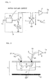
- Fig. 1 shows a circuit block diagram of an example of a photoelectric conversion integrated circuit device embodying the present invention.
- reference numeral 1 represents a photodiode, which has two terminals T 1 and T 2 at its cathode (output), and which outputs a current signal in accordance with a light signal it receives.
- the photodiode 1 has its output terminal T 1 connected to an I/V conversion circuit 2, and has its output terminal T 2 connected to a test circuit 3. Note that such elements as are found also in the conventional example described previously are identified with the same reference numerals and symbols, and overlapping descriptions will not be repeated.
- Fig. 2 shows a section of the chip of the photodiode 1.
- the photodiode 1 has a substrate P - (high-resistance P-type semiconductor) and an epitaxial layer N - (high-resistance N-type semiconductor).
- the substrate P - is used as an anode, and a low-resistance region N within the epitaxial layer N - is used as a cathode.
- the two terminals T 1 and T 2 are kept in contact with the region N.
- the substrate P - is connected to ground via art electrode D.
- the current always flows by way of the wiring H 1 connecting the photodiode 1 to the I/V conversion circuit 2 and by way of the output layer (cathode N) of the photodiode 1.
- the wiring H 1 connecting the photodiode 1 to the I/V conversion circuit 2 and the wiring H 2 connecting the photodiode 1 to the test circuit 3 are arranged too close to each other, there is a strong possibility of a current flowing between the I/V conversion circuit 2 and the test circuit 3 without flowing by way of the wiring H 1 connecting the photodiode 1 to the I/V conversion circuit 2 and by way of the output layer (cathode N) of the photodiode 1.
- the two terminals T 1 and T 2 provided on the output layer of the photodiode 1, with as long a distance (indicated by d in Fig. 2) as possible secured between them.
- the light-sensing device may be provided with three or more output terminals.
- the light-sensing device may be provided with three output terminals.
- one of those three terminals is connected to the I/V conversion circuit 2, and the other two are individually connected, through two separate switching devices 31 and 31' that are controlled by a switch driving circuit 33', to two separate constant-current circuits 32 and 32' that output different amounts of current.
- This allows one of three types of input current to the I/V conversion circuit 2, and thus makes it possible to conduct a versatile functioning check.
- a photoelectric conversion integrated circuit device in a photoelectric conversion integrated circuit device, it is possible to detect a fault in the wiring connecting a light-sensing device to an I/V conversion circuit by feeding a current to the I/V conversion circuit without shining light on the light-sensing device. This helps enhance the reliability of the photoelectric conversion integrated circuit device. Accordingly, such a photoelectric conversion integrated circuit device is suitable for use in a pickup device for a compact disc player, digital video disc player, magneto-optical disc player, or the like.
Landscapes
- Engineering & Computer Science (AREA)
- Multimedia (AREA)
- Signal Processing (AREA)
- Health & Medical Sciences (AREA)
- Biomedical Technology (AREA)
- General Health & Medical Sciences (AREA)
- Solid State Image Pick-Up Elements (AREA)
- Light Receiving Elements (AREA)
- Testing Of Individual Semiconductor Devices (AREA)
- Photometry And Measurement Of Optical Pulse Characteristics (AREA)
- Semiconductor Integrated Circuits (AREA)
- Transforming Light Signals Into Electric Signals (AREA)
- Amplifiers (AREA)
Abstract
Description
Claims (7)
- A photoelectric conversion integrated circuit device for converting a light signal into a voltage signal, said photoelectric conversion integrated circuit device having a light-sensing device that outputs a current in accordance with a light signal it receives, a current-to-voltage conversion circuit that outputs a voltage signal in accordance with a current signal it receives, and a test circuit that outputs a current in accordance with a drive signal fed from outside,wherein a plurality of terminals are provided at an output of said light-sensing device, one of said terminals being connected to said current-to-voltage conversion circuit and at least one of the remainder of said terminals being connected to said test circuit.
- A photoelectric conversion integrated circuit device as claimed in claim 1,wherein a temperature characteristic of conversion efficiency of said current-to-voltage conversion circuit is reverse to a temperature characteristic of an output of said test circuit.
- A photoelectric conversion integrated circuit device as claimed in claim 1,wherein a wiring connecting an output terminal of said light-sensing device to said current-to-voltage conversion circuit and a wiring connecting the output terminal of said light-sensing device to said test circuit are arranged as far away as possible from each other so as to prevent a direct flow of current between those two wirings.
- A photoelectric conversion integrated circuit device as claimed in claim 3,wherein a temperature characteristic of conversion efficiency of said current-to-voltage conversion circuit is reverse to a temperature characteristic of an output of said test circuit.
- A photoelectric conversion integrated circuit device as claimed in claim 1,wherein, among said plurality of terminals provided at the output of said light-sensing device, the terminal connected to an input side of said current-to-voltage conversion circuit and the terminal connected to said test circuit are arranged as far away as possible from each other so as to prevent a direct flow of current between those two terminals.
- A photoelectric conversion integrated circuit device as claimed in claim 5,wherein a temperature characteristic of conversion efficiency of said current-to-voltage conversion circuit is reverse to a temperature characteristic of an output of said test circuit.
- A photoelectric conversion integrated circuit device as claimed in claim 1,wherein a photodiode is composed of a semiconductor substrate and first and second terminals that are kept in contact with a first conducting layer formed within the substrate so as to exhibit conduction reverse to that of the substrate, andwherein a photodiode current flows from the first terminal to a second conducting layer, then to the first conducting layer, and then to the substrate, and a test current flows from the first terminal to the second conducting layer, and then to the second terminal.
Applications Claiming Priority (3)
| Application Number | Priority Date | Filing Date | Title |
|---|---|---|---|
| JP08476197A JP4739467B2 (en) | 1997-04-03 | 1997-04-03 | Photoelectric conversion IC |
| JP8476197 | 1997-04-03 | ||
| PCT/JP1998/001550 WO1998044563A1 (en) | 1997-04-03 | 1998-04-02 | Photoelectric conversion integrated circuit device |
Publications (3)
| Publication Number | Publication Date |
|---|---|
| EP0975025A1 true EP0975025A1 (en) | 2000-01-26 |
| EP0975025A4 EP0975025A4 (en) | 2001-06-20 |
| EP0975025B1 EP0975025B1 (en) | 2006-11-02 |
Family
ID=13839675
Family Applications (1)
| Application Number | Title | Priority Date | Filing Date |
|---|---|---|---|
| EP98911201A Expired - Lifetime EP0975025B1 (en) | 1997-04-03 | 1998-04-02 | Photoelectric conversion integrated circuit device |
Country Status (7)
| Country | Link |
|---|---|
| US (1) | US6316955B1 (en) |
| EP (1) | EP0975025B1 (en) |
| JP (1) | JP4739467B2 (en) |
| KR (1) | KR100502057B1 (en) |
| CN (1) | CN1159767C (en) |
| DE (1) | DE69836322T2 (en) |
| WO (1) | WO1998044563A1 (en) |
Cited By (2)
| Publication number | Priority date | Publication date | Assignee | Title |
|---|---|---|---|---|
| WO2003007004A1 (en) * | 2001-07-12 | 2003-01-23 | Em Dicroelectronic-Marin Sa | Injection current test circuit |
| EP2416560A4 (en) * | 2009-04-01 | 2013-06-05 | Hamamatsu Photonics Kk | SOLID IMAGING ELEMENT AND METHOD FOR MANUFACTURING SAME, RADIATION IMAGING DEVICE AND METHOD FOR MANUFACTURING SAME, AND INSPECTION METHOD FOR SOLID IMAGING ELEMENT |
Families Citing this family (14)
| Publication number | Priority date | Publication date | Assignee | Title |
|---|---|---|---|---|
| DE10220306C1 (en) * | 2002-05-07 | 2003-12-11 | Kostal Leopold Gmbh & Co Kg | Electrical circuit arrangement and method for checking the integrity of a photodiode array |
| CN100347858C (en) * | 2002-10-31 | 2007-11-07 | 上海华虹集成电路有限责任公司 | Photo detection circuit |
| JP5066791B2 (en) * | 2005-06-30 | 2012-11-07 | ミツミ電機株式会社 | Light receiving device and light receiving device inspection method |
| JP4159582B2 (en) | 2006-04-26 | 2008-10-01 | 松下電器産業株式会社 | Test circuit and test method for photoreceiver / amplifier circuit |
| JP2008070277A (en) * | 2006-09-15 | 2008-03-27 | Matsushita Electric Ind Co Ltd | Inspection circuit for current-voltage conversion amplifier and optical pickup device using the same |
| US8309901B2 (en) * | 2007-05-18 | 2012-11-13 | Sharp Kabushiki Kaisha | Display device adjusting luminance of display based at least on detections by ambient light sensors |
| US8368676B2 (en) * | 2007-05-18 | 2013-02-05 | Sharp Kabushiki Kaisha | Display device with light shield |
| JP5073741B2 (en) * | 2007-05-18 | 2012-11-14 | シャープ株式会社 | Display device |
| JP4380732B2 (en) | 2007-06-04 | 2009-12-09 | セイコーエプソン株式会社 | Detection circuit, vibration-type gyro sensor circuit, vibration-type gyro sensor, and electronic device |
| US20100283474A1 (en) * | 2009-05-11 | 2010-11-11 | Panasonic Corporation | Test circuit and optical pickup device |
| CN110519534B (en) * | 2018-11-08 | 2021-05-28 | 神盾股份有限公司 | Current-driven pixel circuits and associated image sensors |
| CN112433172A (en) * | 2019-08-08 | 2021-03-02 | 鸿富锦精密工业(武汉)有限公司 | Power failure detection device |
| JP2022173796A (en) * | 2021-05-10 | 2022-11-22 | ソニーセミコンダクタソリューションズ株式会社 | IMAGE SENSOR, IMAGING DEVICE, AND IMAGE SENSOR CONTROL METHOD |
| USD1066192S1 (en) * | 2023-09-01 | 2025-03-11 | Volvo Truck Corporation | Door for vehicle |
Family Cites Families (6)
| Publication number | Priority date | Publication date | Assignee | Title |
|---|---|---|---|---|
| CA997481A (en) * | 1972-12-29 | 1976-09-21 | International Business Machines Corporation | Dc testing of integrated circuits and a novel integrated circuit structure to facilitate such testing |
| US4241358A (en) * | 1979-03-26 | 1980-12-23 | Trw Inc. | Radiation sensitive device with lateral current |
| JPS6313368A (en) | 1986-07-04 | 1988-01-20 | Canon Inc | Semiconductor sensor device |
| JP2793085B2 (en) * | 1992-06-25 | 1998-09-03 | 三洋電機株式会社 | Optical semiconductor device and its manufacturing method |
| JP3203996B2 (en) * | 1994-11-01 | 2001-09-04 | 三菱電機株式会社 | Test circuit for current-voltage conversion amplifier |
| US5592124A (en) * | 1995-06-26 | 1997-01-07 | Burr-Brown Corporation | Integrated photodiode/transimpedance amplifier |
-
1997
- 1997-04-03 JP JP08476197A patent/JP4739467B2/en not_active Expired - Fee Related
-
1998
- 1998-04-02 US US09/381,964 patent/US6316955B1/en not_active Expired - Fee Related
- 1998-04-02 EP EP98911201A patent/EP0975025B1/en not_active Expired - Lifetime
- 1998-04-02 WO PCT/JP1998/001550 patent/WO1998044563A1/en not_active Ceased
- 1998-04-02 KR KR10-1999-7008845A patent/KR100502057B1/en not_active Expired - Fee Related
- 1998-04-02 DE DE69836322T patent/DE69836322T2/en not_active Expired - Lifetime
- 1998-04-02 CN CNB988036177A patent/CN1159767C/en not_active Expired - Fee Related
Cited By (4)
| Publication number | Priority date | Publication date | Assignee | Title |
|---|---|---|---|---|
| WO2003007004A1 (en) * | 2001-07-12 | 2003-01-23 | Em Dicroelectronic-Marin Sa | Injection current test circuit |
| EP2416560A4 (en) * | 2009-04-01 | 2013-06-05 | Hamamatsu Photonics Kk | SOLID IMAGING ELEMENT AND METHOD FOR MANUFACTURING SAME, RADIATION IMAGING DEVICE AND METHOD FOR MANUFACTURING SAME, AND INSPECTION METHOD FOR SOLID IMAGING ELEMENT |
| US8975591B2 (en) | 2009-04-01 | 2015-03-10 | Hamamatsu Photonics K.K. | Solid-state imaging device and method of manufacturing the same, radiological imaging apparatus and method of manufacturing the same, and method of testing solid-state imaging device |
| KR101615788B1 (en) | 2009-04-01 | 2016-04-26 | 하마마츠 포토닉스 가부시키가이샤 | Solid imaging element and production method therefor, radiation imaging device and production method therefor, and inspection method for solid imaging element |
Also Published As
| Publication number | Publication date |
|---|---|
| US6316955B1 (en) | 2001-11-13 |
| CN1251208A (en) | 2000-04-19 |
| KR20010005773A (en) | 2001-01-15 |
| CN1159767C (en) | 2004-07-28 |
| EP0975025A4 (en) | 2001-06-20 |
| JPH10284707A (en) | 1998-10-23 |
| DE69836322D1 (en) | 2006-12-14 |
| KR100502057B1 (en) | 2005-07-25 |
| JP4739467B2 (en) | 2011-08-03 |
| EP0975025B1 (en) | 2006-11-02 |
| WO1998044563A1 (en) | 1998-10-08 |
| DE69836322T2 (en) | 2007-06-28 |
Similar Documents
| Publication | Publication Date | Title |
|---|---|---|
| US6316955B1 (en) | Photoelectric conversion integrated circuit device | |
| US5034600A (en) | Detection output circuit for a photoelectric switch integrated circuit with reduced interconnections | |
| US5115124A (en) | Semiconductor photosensor having unitary construction | |
| US7642494B2 (en) | Light emitting apparatus and method for inspecting same | |
| KR100444121B1 (en) | Sensor device | |
| US7326905B2 (en) | Photodetector and optical receiver | |
| US20100283474A1 (en) | Test circuit and optical pickup device | |
| JP3837372B2 (en) | Semiconductor relay | |
| JPH0792075A (en) | Particle detection circuit | |
| US5977571A (en) | Low loss connecting arrangement for photodiodes | |
| US20080211512A1 (en) | Test circuit arrangement and testing method for testing of a circuit section | |
| US7800038B2 (en) | Photodetector device | |
| KR100281739B1 (en) | Reliability Selection Circuit of Photodiode for Optical Communication | |
| US20090050788A1 (en) | System for Sequentially Measuring the Output of a Plurality of Light Sensors Which Generate Current in Response to Incident Light | |
| JPH09138161A (en) | Photodetector | |
| JP2005340517A (en) | Laser module | |
| JP2715603B2 (en) | Semiconductor device | |
| JPH07114330B2 (en) | Light receiving circuit range switching circuit | |
| KR960001348B1 (en) | Close image sensor | |
| JPH11326044A (en) | Sensor device | |
| JPS61125076A (en) | Image sensor and manufacture thereof | |
| JPS6225511A (en) | Semiconductor relay | |
| JPS60165859A (en) | Image sensor | |
| JPH0529920A (en) | Solid-state relay | |
| JP2001007980A (en) | Document reading apparatus and operation method thereof |
Legal Events
| Date | Code | Title | Description |
|---|---|---|---|
| PUAI | Public reference made under article 153(3) epc to a published international application that has entered the european phase |
Free format text: ORIGINAL CODE: 0009012 |
|
| 17P | Request for examination filed |
Effective date: 19990930 |
|
| AK | Designated contracting states |
Kind code of ref document: A1 Designated state(s): DE FR GB IT NL |
|
| A4 | Supplementary search report drawn up and despatched |
Effective date: 20010508 |
|
| AK | Designated contracting states |
Kind code of ref document: A4 Designated state(s): DE FR GB IT NL |
|
| GRAP | Despatch of communication of intention to grant a patent |
Free format text: ORIGINAL CODE: EPIDOSNIGR1 |
|
| GRAS | Grant fee paid |
Free format text: ORIGINAL CODE: EPIDOSNIGR3 |
|
| GRAA | (expected) grant |
Free format text: ORIGINAL CODE: 0009210 |
|
| AK | Designated contracting states |
Kind code of ref document: B1 Designated state(s): DE FR GB IT NL |
|
| PG25 | Lapsed in a contracting state [announced via postgrant information from national office to epo] |
Ref country code: IT Free format text: LAPSE BECAUSE OF FAILURE TO SUBMIT A TRANSLATION OF THE DESCRIPTION OR TO PAY THE FEE WITHIN THE PRESCRIBED TIME-LIMIT;WARNING: LAPSES OF ITALIAN PATENTS WITH EFFECTIVE DATE BEFORE 2007 MAY HAVE OCCURRED AT ANY TIME BEFORE 2007. THE CORRECT EFFECTIVE DATE MAY BE DIFFERENT FROM THE ONE RECORDED. Effective date: 20061102 |
|
| REG | Reference to a national code |
Ref country code: GB Ref legal event code: FG4D |
|
| REF | Corresponds to: |
Ref document number: 69836322 Country of ref document: DE Date of ref document: 20061214 Kind code of ref document: P |
|
| EN | Fr: translation not filed | ||
| PLBE | No opposition filed within time limit |
Free format text: ORIGINAL CODE: 0009261 |
|
| STAA | Information on the status of an ep patent application or granted ep patent |
Free format text: STATUS: NO OPPOSITION FILED WITHIN TIME LIMIT |
|
| 26N | No opposition filed |
Effective date: 20070803 |
|
| PG25 | Lapsed in a contracting state [announced via postgrant information from national office to epo] |
Ref country code: FR Free format text: LAPSE BECAUSE OF FAILURE TO SUBMIT A TRANSLATION OF THE DESCRIPTION OR TO PAY THE FEE WITHIN THE PRESCRIBED TIME-LIMIT Effective date: 20070615 |
|
| PG25 | Lapsed in a contracting state [announced via postgrant information from national office to epo] |
Ref country code: FR Free format text: LAPSE BECAUSE OF FAILURE TO SUBMIT A TRANSLATION OF THE DESCRIPTION OR TO PAY THE FEE WITHIN THE PRESCRIBED TIME-LIMIT Effective date: 20061102 |
|
| PGFP | Annual fee paid to national office [announced via postgrant information from national office to epo] |
Ref country code: GB Payment date: 20100325 Year of fee payment: 13 |
|
| PGFP | Annual fee paid to national office [announced via postgrant information from national office to epo] |
Ref country code: NL Payment date: 20100416 Year of fee payment: 13 Ref country code: DE Payment date: 20100430 Year of fee payment: 13 |
|
| REG | Reference to a national code |
Ref country code: DE Ref legal event code: R119 Ref document number: 69836322 Country of ref document: DE |
|
| REG | Reference to a national code |
Ref country code: DE Ref legal event code: R119 Ref document number: 69836322 Country of ref document: DE |
|
| REG | Reference to a national code |
Ref country code: NL Ref legal event code: V1 Effective date: 20111101 |
|
| GBPC | Gb: european patent ceased through non-payment of renewal fee |
Effective date: 20110402 |
|
| PG25 | Lapsed in a contracting state [announced via postgrant information from national office to epo] |
Ref country code: NL Free format text: LAPSE BECAUSE OF NON-PAYMENT OF DUE FEES Effective date: 20111101 |
|
| PG25 | Lapsed in a contracting state [announced via postgrant information from national office to epo] |
Ref country code: GB Free format text: LAPSE BECAUSE OF NON-PAYMENT OF DUE FEES Effective date: 20110402 |
|
| PG25 | Lapsed in a contracting state [announced via postgrant information from national office to epo] |
Ref country code: DE Free format text: LAPSE BECAUSE OF NON-PAYMENT OF DUE FEES Effective date: 20111031 |