EP0971434B1 - Zusammengesetzter Schaltkreis und Schaltgerät dazu - Google Patents
Zusammengesetzter Schaltkreis und Schaltgerät dazu Download PDFInfo
- Publication number
- EP0971434B1 EP0971434B1 EP19980112502 EP98112502A EP0971434B1 EP 0971434 B1 EP0971434 B1 EP 0971434B1 EP 19980112502 EP19980112502 EP 19980112502 EP 98112502 A EP98112502 A EP 98112502A EP 0971434 B1 EP0971434 B1 EP 0971434B1
- Authority
- EP
- European Patent Office
- Prior art keywords
- circuit
- diode
- transmission line
- composite switch
- capacitor
- Prior art date
- Legal status (The legal status is an assumption and is not a legal conclusion. Google has not performed a legal analysis and makes no representation as to the accuracy of the status listed.)
- Expired - Lifetime
Links
- 239000002131 composite material Substances 0.000 title claims description 66
- 239000003990 capacitor Substances 0.000 claims description 58
- 239000000758 substrate Substances 0.000 claims description 50
- 230000005540 biological transmission Effects 0.000 claims description 46
- 238000010586 diagram Methods 0.000 description 10
- 238000003780 insertion Methods 0.000 description 9
- 230000037431 insertion Effects 0.000 description 9
- 238000004891 communication Methods 0.000 description 4
- 230000001413 cellular effect Effects 0.000 description 3
- 238000010276 construction Methods 0.000 description 3
- 239000003989 dielectric material Substances 0.000 description 2
- 239000004065 semiconductor Substances 0.000 description 2
- 239000004020 conductor Substances 0.000 description 1
- 230000003247 decreasing effect Effects 0.000 description 1
- 230000001419 dependent effect Effects 0.000 description 1
- 238000010304 firing Methods 0.000 description 1
- 238000002955 isolation Methods 0.000 description 1
- 239000003550 marker Substances 0.000 description 1
- 238000007650 screen-printing Methods 0.000 description 1
- 230000001629 suppression Effects 0.000 description 1
Images


Classifications
-
- H—ELECTRICITY
- H01—ELECTRIC ELEMENTS
- H01P—WAVEGUIDES; RESONATORS, LINES, OR OTHER DEVICES OF THE WAVEGUIDE TYPE
- H01P1/00—Auxiliary devices
- H01P1/10—Auxiliary devices for switching or interrupting
- H01P1/15—Auxiliary devices for switching or interrupting by semiconductor devices
Definitions
- the present invention relates to a switch circuit, and particularly to a composite switch circuit comprising a diode switch circuit incorporated with a low pass filter circuit for use as a high frequency switch circuit of a digital cellular radiotelephone, etc. to alternately switch transmission paths for transmitting or receiving communication signals.
- the present invention relates also to a composite switch device of an integral multi-layer body including the composite switch circuit.
- a switch circuit for a digital cellular radiotelephone, etc. is utilized to alternately connect a receiving circuit to an antenna or a transmitting circuit to the antenna.
- the switch circuit In a radiotelephone employing a reception diversity system, the switch circuit also alternately connects a receiving circuit to a first antenna or the receiving circuit to a second antenna.
- the switch circuit is also utilized to alternately connect a transmitting circuit to a first antenna or the transmitting circuit to a second antenna.
- the switch circuit is also used for switching a path to an internal circuit and a path to the external port. Further, the switch circuit is used for switching a plurality of channels of base stations for the radio communication system.
- Fig. 11 is a schematic circuit diagram showing a conventional switch circuit disclosed in Japanese Patent Laid-Open No. 6-197040.
- the switch circuit alternately connects a transmitting circuit Tx to an antenna ANT or a receiving circuit Rx to the antenna ANT.
- the transmitting circuit Tx is connected to an anode of a first diode D101 via a first capacitor C101.
- a cathode of the first diode D101 is connected to the antenna ANT via a third capacitor C103.
- the antenna ANT is also connected to a receiving circuit Rx via series-connected third capacitor C103, second transmission line SL2 and fourth capacitor C104.
- An anode of the first diode D101 is grounded via series-connected first transmission line SL1 and second capacitor C102.
- a control circuit T1 is connected to a node formed between the first transmission line SL1 and the second capacitor C102 via a resistance R101.
- An anode of a second diode D102 is connected to a node formed between the second transmission line SL2 and the fourth capacitor C104, and a cathode thereof is grounded.
- the transmission lines and some of the capacitors are disposed on a plurality of substrates of a dielectric laminate body, and the diodes, resistance and the other of the capacitors are mounted on a top surface of the laminate body.
- EP 0 785 590 A discloses a composite device including a switch circuit and a filter circuit. This device has the features included in the first part of claim 1.
- An equivalent circuit of the composite device is shown in Fig. 12.
- a filter circuit portion is represented by a block shown in broken line.
- the filter circuit is positioned to interconnect a transmitting circuit Tx and the switch circuit.
- An equivalent circuit when the transmitting circuit Tx is electrically connected to the antenna ANT is shown in Fig. 13.
- the diodes D201 and D202 are not shown because they are on position by DC current and in low impedance state to form short circuits.
- a conventional circuit formed by simply connecting the filter circuit to the switch circuit lacks symmetry in the circuit configuration to exhibit a sufficient frequency characteristics only in a narrow frequency band.
- a narrow-band switch circuit is of less performance in view of the full utilization of the frequency band allocated for a communication system, and is poor in productivity due to the variability of products.
- an object of the present invention is to provide a broad band, composite switch circuit with a high symmetry in the circuit configuration and a miniaturized composite switch device of an integral multi-layer structure including the composite switch circuit.
- the inventors have found that the symmetry in the circuit configuration can be increased by disposing a low pass filter circuit between a diode and a transmission line in a switch circuit in stead of simply connecting the low pass filter circuit to the switch circuit, thereby decreasing the level of insertion loss and ensuring a high performance of the switch circuit in a broader frequency band as compared with conventionally known switch circuits.
- the composite switch circuit of the present invention is a switch circuit incorporated with a low pass filter circuit, and is operable to alternately and electrically connecting a first circuit to a third circuit or a second circuit to the third circuit
- the composite switch circuit may be an antenna switch circuit in which the first circuit is a transmitting circuit, the second circuit is a receiving circuit, and the third circuit is an antenna.
- the present invention will be described more in detail with respect to such an antenna switch circuit. However, it should be considered to illustrate one of various preferred embodiments of the present invention.
- a circuit for a low pass filter circuit is incorporated into a switch circuit to form a single composite switch circuit.
- the composite switch circuit may be disposed on a plurality of dielectric substrates to form a miniaturized composite switch device of an integral multi-layer body.
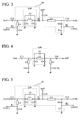
- FIG. 3 An equivalent circuit of a radio transceiver circuit including a composite switch circuit of the present invention is shown in Fig. 3.
- the first circuit is a transmitting circuit Tx
- the second circuit is a receiving circuit Rx
- the third circuit is an antenna ANT.
- a composite switch circuit 30 within a block indicated by broken line includes a first path interconnecting the transmitting circuit Tx and the antenna ANT and a second path interconnecting the receiving circuit Rx and the antenna ANT.
- the first path includes a first diode D1 and a first transmission line L1, a first side portion of the first diode D1 being connected to the antenna ANT and a first side portion of the first transmission line L1 being connected to a node between a second side portion of the first diode D1 and the transmitting circuit Tx in a shunt configuration.
- the second path includes a second transmission line L2 and a second diode D2, a first side portion of the second transmission line L2 being connected to the antenna ANT and a first side portion of the second diode D2 being connected to a node between a second side portion of the second transmission line L2 and the receiving circuit Rx in a shunt configuration.
- the low pass filter circuit LPF within a block indicated by broken line is incorporated into the switch circuit so as to interconnect the second side portion of the first diode D1 and the first side portion of the shunt-connected first transmission line L1, thereby to form the composite switch circuit of the present invention.
- the low pass filter circuit LPF usually comprises a transmission line L3, a capacitor C4 in parallel to the transmission line L3, and capacitors C2 and C3 each forming a shunt path to ground.
- a second side portion of the transmission line L1 is grounded via a capacitor C14, and a first control circuit CONT1 is shunt-connected between the first transmission line L1 and the capacitor C14 via a resistance R1.
- the CONT1 may be omitted, and if omitted, the first transmission- line L1 may be directly grounded.
- a second side portion of the second diode D2 is grounded via a capacitor C1, and a second control circuit CONT2 is shunt-connected between the second diode D2 and the capacitor C1 via a resistance R2.
- the control circuits control whether the transmitting circuit Tx (first circuit) or the receiving circuit Rx (second circuit) is electrically connected to the antenna ANT (third circuit) by biasing the diodes D1 and D2.
- a DC cutting capacitor C11, C12 or C13 To each input/output terminal of the transmitting circuit Tx, the receiving circuit Rx and the antenna ANT, connected is a DC cutting capacitor C11, C12 or C13 for passing only high frequency signals therethrough.
- the low pass filter circuit is not simply connected to a switch circuit, but is incorporated into the switch circuit, more specifically, is incorporated between the second side portion of the first diode D1 and the first side portion of the shunt-connected first transmission line L1.
- An equivalent circuit of Fig. 3 when the transmitting circuit Tx is electrically connected to the antenna ANT is shown in Fig. 4.
- the diodes D1 and D2 are not shown because they are in a highly conducting, low impedance state to form short circuits.
- the composite switch circuit of the present invention is highly symmetric in the circuit configuration. Namely, the transmitting circuit Tx, the capacitor C11, the transmission line L1 and the capacitor C14 are positioned symmetrically with the antenna ANT, the capacitor C13, the transmission line L2 and the capacitor C1(C12), respectively, with respect to the central low pass filter circuit. With such a symmetry in the circuit configuration, the composite switch circuit of the present invention exhibits a lower level of insertion loss and sufficient characteristics in a broader frequency band as compared with conventional switch circuits.
- FIG. 5 An equivalent circuit of another composite switch circuit 50 of the present invention is shown in Fig. 5.
- the equivalent circuit of Fig. 5 is similar to that of Fig. 3, but in which the first and second diodes D1 and D2 are reversely connected with respect to anode and cathode.
- the circuit of Fig. 5 has the same equivalent circuit as shown in Fig. 4.
- the composite switch circuit of Fig. 5 has also a high symmetry in the circuit configuration, and exhibits a lower level of insertion loss and sufficient characteristics in a broader frequency band as compared with conventional switch circuits.
- the equivalent circuit of Fig. 3 has been experimentally confirmed to have a lower level of insertion loss and a good isolation as compared with the equivalent circuit of Fig. 5.
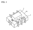
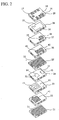
- Fig. 1 is a perspective view showing a composite switch device of the present invention. Substrates constructing the integral multi-layer body of the composite switch device of Fig. 1 are perspectively shown in Fig. 2, and an equivalent circuit of a composite switch circuit disposed on a plurality of dielectric substrates of the composite switch device of Figs. 1 and 2 is shown in Fig. 3.
- the composite switch device comprises a semiconductor element 1 containing two diodes and an integral multi-layer body 2 of a plurality of dielectric substrates.
- a portion indicating the electrodes are shown by hatch makings.
- the composite switch circuit of the present invention comprises the elements contained within the block 30 indicated by broken line, and capacitors C11, C12, C13, C14 and the resistances R1 and R2 outside the block 30 are external elements which may be formed on a circuit board on which the composite switch device is mounted, or may be disposed on the dielectric substrates or the top surface of the integral multi-layer body.
- the composite switch device of the embodiment comprises a bottom dielectric substrate 21, inner substrates 22-28 and a top dielectric substrate 29.
- a first ground electrode 31 is formed, from which lead electrodes extend to be connected to external electrodes T2, T7 and T8 on the side surface of the integral multi-layer body 2.
- a capacitor electrode 41 opposing the first ground electrode 31 is formed so as to form the capacitor C1.
- a lead electrode extending from the capacitor electrode 41 is connected to an external electrode T4.
- the capacitor C1 is formed inside the integral multi-layer body in this embodiment, it may be externally formed, for example, on the top surface of the top dielctric surbstrate 29 or on the circuit board on which the composite switch device is mounted.
- a spiral line electrode 11 on the dielectric substrate 23 is connected to a spiral line electrode 12 on the dielectric substrate 24 via a through-hole electrode 51 to form the transmission line L1.
- Two lead electrodes extend from the spiral line electrodes 11 and 12 to be respectively connected to external electrodes T3 and T6.
- a spiral line electrode 13 on the dielectric substrate 23 is connected to a spiral line electrode 14 on the dielectric substrate 24 via a through-hole electrode 52 to form the transmission line L2.
- Two lead electrodes extend from the spiral line electrodes 13 and 14 to be respectively connected to external electrodes T5 and T1.
- a second ground electrode 32 is formed on the top surface of a dielectric substrate 25 laminated on the dielectric substrate 24 .
- Three lead electrodes extend from the second ground electrode 32 to be respectively connected to the external electrodes T2, T7 and T8.
- a dielectric substrate 26 is laminated on the dielectric substrate 25, a dielectric substrate 26 is laminated. On the top surface the dielectric substrate 26, a capacitor electrode 42 opposing the second ground electrode 32 is formed to form the capacitor C2 of the low pass filter circuit. Also formed on the dielectric substrate 26 is a capacitor electrode 43 opposing the second ground electrode 32 to form the capacitor C3 of the low pass filter circuit. From the capacitor electrode 42, a lead electrode extends to be connected to the external electrode T3.
- a capacitor electrode 44 opposing the capacitor electrode 42 of the dielectric substrate 26 is formed on the top surface of a dielectric substrate 27 to form the capacitor C4 of the low pass filter circuit.
- the capacitor electrode 44 is connected to the capacitor electrode 43 on the dielectric substrate 26 via a through-hole 53.
- a spiral line electrode 15 forming the transmission line L3 of the low pass filter circuit is formed on the top surface of the dielectric substrate 28, a spiral line electrode 15 forming the transmission line L3 of the low pass filter circuit is formed. An end of the spiral line electrode is connected to the external electrode T3, and the opposite end is connected to the capacitor electrodes 44 and 43 via the through-holes 54 and 53.
- pattern electrodes 16 and 17 are formed on the top surface of the top dielectric substrate 29 .
- the pattern electrode 16 is connected to the through-hole 54 on the dielectric substrate 28 via a through-hole 55.
- the pattern electrode 17 serves as a marker.
- pattern electrodes to be connected to the external electrodes T1, T4, T5 and T6 are further formed.
- An composite switch device having the above construction was produced by using dielectric material having a dielectric constant of about 8.
- the dielectric material was made into a sheet form (dielectric substrates) by a doctor blade and respective pattern electrodes were formed on the dielectric sheets by screen-printing an electrically conductive material such as Ag.
- the dielectric substrates having thereon pattern electrodes printed were laminated, compressed and fired to an integral multi-layer body. After firing, the external electrodes T1 to T8 and the pattern electrodes were formed on the side surface and the top surface of the integral multi-layer body.
- the semiconductor element 1 containing the first and second diodes D1 and D2 was mounted on the top surface of the integral multi-layer body so that the first diode D1 was connected to the pattern electrode 16 and the external electrodes T5, and the second diode D2 was connected to the external electrodes T1 and T4, respectively, to obtain a composite switch device of the present invention of a size having length/width of 4.5 mm/3.2 mm and a thickness of 2 mm.
- the low pass filter circuit comprising the capacitors C2, C3 and C4 and the transmission line L3 was inserted between the anode portion of the first diode D1 and the first side portion of the shunt-connected transmission line L1.
- a radio transceiver circuit of Fig. 3 is obtained by connecting the transmitting circuit Tx to the external electrode T3 via the capacitor Cell, connecting the antenna ANT to the external electrode T5 via the capacitor C13, connecting the receiving circuit Rx to the external electrode T1 via the capacitor 12, connecting the first control circuit CONT1 to the external electrode T6 via the resistance R1, connecting the capacitor C14 to the external electrode T6 to form a path to ground, and connecting the second control circuit CONT2 to the external electrode T4 via the resistance R2.
- the insertion loss at a frequency up to 5.5 GHz measured on the composite switch device obtained above is shown in Fig. 6A.
- An enlarged representation of the passband (0.5 to 1.5 GHz) of Fig. 6A is shown in Fig. 6B.
- the composite switch device exhibited an insertion loss as low as 1 dB or less at a frequency range of 900 ⁇ 250 MHz.
- the composite switch circuit of the preferred embodiment of the present invention is excellent in minimizing the insertion loss.
- the geometrical size can be reduce, only a small space is required in mounting the composite switch device of the present invention on a circuit board, thereby reducing the size of a radio transceiver such as a cellular radiotelephone.
- the composite switch device of the present invention is suitably used in a frequency range of about 800 MHz to several gigas of hertz.
- the first and second transmission lines L1 and L2 were disposed between the first ground electrode 31 and the second ground electrode 32, and a substantial part of the switch circuit portion is disposed nearer to the mounting surface than the low pass filter circuit portion.
- the second ground electrode 32 forming the grounded capacitors C2 and C3 with the opposing capacitor electrodes 42 and 43 may have a lead portion, i.e. the external electrode T2 in the above embodiment, to be connected to a ground terminal of a circuit board on which the composite switch device is mounted.
- the external electrode T2 functions as a line electrode which may be considered as inductors L4 and L5, as shown by an equivalent circuit of Fig. 7, connected to the capacitors C2 and C3 in series. In such an equivalent circuit, harmonics can be effectively reduced by the series resonance between the capacitor C2 with the inductor L4, and the capacitor C3 with the inductor L5.
- the first and second transmission lines L1 and L2 are disposed between two ground electrodes, and that the capacitor of the low pass filter circuit is formed by the ground electrode above the transmission lines L1 and L2 and the capacitor electrode above and opposing the ground electrode.
- the transmission lines L1 and L2 were formed by spiral line electrodes printed on successively adjacent two dielectric substrates. By making the line electrodes spiral and partially overlapping the line electrodes on the tow dielectric substrates, the length of the line electrodes were made shorter.
- Fig. 8 is a perspective view showing respective substrates constructing an integral multi-layer body disposed by another composite switch circuit 90 of the present invention.
- An equivalent circuit including the composite switch circuit 90 is shown in Fig. 9.
- the equivalent circuit of Fig. 9 is similar to that of Fig. 2, but in which an additional capacitor C5 is connected between the low pass filter circuit and the shunt-connected first transmission line L1 to form a shunt path to ground.
- the capacitor C5 is formed by a first ground electrode 31 on a dielectric substrate 21 and a capacitor electrode 45 on a dielectric substrate 22 which is connected to an external electrode T3. Since the third to ninth substrates from the bottom of Fig. 8 are respectively the same as the dielectric substrates 23 to 29 of Fig. 2, the description of these substrates are omitted here and in Fig. 8.
- a composite switch device including the above composite switch circuit was produced in the same manner as described above, and was confirmed to have the same performance as in the above embodiment.
- an additional capacitor C6 may be connected as shown in Fig. 10.
- the line length of the first transmission line L1 can be effectively made shorter.
- a small composite switch circuit which is incorporated with a low pass filter circuit, having a high performance can be obtained.
- a miniaturized composite switch device including the composite switch circuit can be obtained in a form of an integral multi-layer body by disposing the composite switch circuit on a plurality of dielectric substrates.
- the composite switch circuit and composite switch device of the present invention exhibit sufficient characteristics in a broad frequency range, much less insertion loss and a high suppression effect of harmonics.
Landscapes
- Transceivers (AREA)
- Waveguide Switches, Polarizers, And Phase Shifters (AREA)
Claims (9)
- Zusammengesetzter Schalterstromkreis (30) zur abwechselnden und elektrischen Verbindung einer Übertragungsschaltung (Tx) oder einer Empfangsschaltung (Rx) mit einer Antenne (ANT), umfassend:einen die Übertragungsschaltung (Tx) und die Antenne (ANT) verbindenden ersten Pfad, wobei der erste Pfad eine erste Diode (D1) und eine erste Übertragungsleitung (L1) enthält, wobei ein Anschluß der ersten Diode (D1) mit der Antenne (ANT) verbunden ist, ein Ende der ersten Übertragungsleitung (L1) mit einem zwischen der Übertragungsschaltung (Tx) und dem anderen Anschluß der ersten Diode (D1) gebildeten Knoten verbunden ist und ihr anderes Ende mit der Masse verbunden ist,einen die Empfangsschaltung (Rx) und die Antenne (ANT) verbindenden zweiten Pfad, wobei der zweite Pfad eine zweite Übertragungsleitung (L2) und eine zweite Diode (D2) enthält, wobei ein Ende der zweiten Übertragungsleitung (L2) mit der Antenne (ANT) verbunden ist, ein Anschluß der zweiten Diode (D2) mit einem zwischen dem anderen Ende der Übertragungsleitung (L2) und der Empfangsschaltung (Rx) gebildeten Knoten verbunden ist und ihr anderer Anschluß mit der Masse verbunden ist, undeine im ersten Pfad angeordnete Tiefpaßfilterschaltung (LPF), die eine Übertragungsleitung (L3) und Kondensatoren umfaßt,dadurch gekennzeichnet, daß die Tiefpaßfilterschaltung (LPF) den anderen Anschluß der ersten Diode (D1) und das eine Ende der ersten Übertragungsleitung (L1) verbindet.
- Schalterstromkreis nach Anspruch 1, wobei der eine Anschluß der ersten Diode ihre Anode ist und der eine Anschluß der zweiten Diode deren Anode ist.
- Schalterstromkreis nach Anspruch 1, wobei der eine Anschluß der ersten Diode ihre Kathode ist und der eine Anschluß der zweiten Diode deren Kathode ist.
- Zusammengesetztes Schaltergerät umfassend den zusammengesetzten Schalterstromkreis (30) nach einem der Ansprüche 1 bis 3, der auf einer Mehrzahl von dielektrischen Substraten auf einem einstückigen Mehrschichtkörper (2) angeordnet ist, wobei zumindest die erste Übertragungsleitung (L1), die zweite Übertragungsleitung (L2) und ein Teil der Tiefpaßfilterschaltung (LPF) auf mindestens einem inneren dielektrischen Substrat (22-28) im einstückigen Mehrschichtkörper (2) angeordnet sind.
- Gerät nach Anspruch 4, wobei die erste und die zweite Diode (D1, D2) auf einer obersten Oberfläche des einstückigen Mehrschichtkörpers (2) angeordnet sind.
- Gerät nach Anspruch 4 oder 5, wobei die erste und die zweite Übertragungsleitung (L1, L2), die auf inneren dielektrischen Substraten (22-28) im einstückigen Mehrschichtkörper (2) angeordnet sind, zwischen zwei auf den jeweiligen dielektrischen Substraten (21, 25) angeordneten Masseelektroden (31, 32) positioniert sind und wobei ein Kondensator (C2) der Tiefpaßfilterschaltung (LPF) durch die eine (32) der beiden Masseelektroden (31, 32), die die erste und die zweite Übertragungsleitung (L1, L2) sandwichartig einfassen, und eine Elektrode (42) die auf einem oberhalb und entgegengesetzt der oberen Massenelektrode (32) positionierten dielektrischen Substrat (26) angeordnet ist, gebildet ist.
- Gerät nach Anspruch 6, wobei Elektroden (32, 42), die Platten des Kondensators (C2) der Tiefpaßfilterschaltung (LPF) bilden, jeweils auf dielektrischen Substraten (25, 26) angeordnet sind, die auf der oberen Seite der ersten und der zweiten Übertragungsleitung (L1, L2) bezüglich einer Montagefläche des zusammengesetzten Schaltergeräts positioniert sind.
- Gerät nach einem der Ansprüche 4 bis 7, wobei die erste und die zweite Übertragungsleitung (L1, L2) durch Elektrodenmuster (11-14) von Spiralenform gebildet sind.
- Gerät nach Anspruch 2 oder der Ansprüche 4 bis 8, sofern diese von Anspruch 2 abhängen, wobei eine Steuerungsschaltung (CONT2) mit der Anode der zweiten Diode (T2) verbunden ist und eine Spannung zwischen den Anoden der ersten und der zweiten Diode (D1, D2) angelegt wird.
Priority Applications (4)
| Application Number | Priority Date | Filing Date | Title |
|---|---|---|---|
| DE69837841T DE69837841T2 (de) | 1998-07-06 | 1998-07-06 | Zusammengesetzter Schaltkreis und Schaltgerät dazu |
| ES98112502T ES2287964T3 (es) | 1998-07-06 | 1998-07-06 | Circuito de conmutacion y dispositivo de conmutacion compuestos. |
| EP19980112502 EP0971434B1 (de) | 1998-07-06 | 1998-07-06 | Zusammengesetzter Schaltkreis und Schaltgerät dazu |
| CN 200410044632 CN1545215B (zh) | 1998-07-06 | 1998-07-20 | 组合切换电路 |
Applications Claiming Priority (1)
| Application Number | Priority Date | Filing Date | Title |
|---|---|---|---|
| EP19980112502 EP0971434B1 (de) | 1998-07-06 | 1998-07-06 | Zusammengesetzter Schaltkreis und Schaltgerät dazu |
Publications (2)
| Publication Number | Publication Date |
|---|---|
| EP0971434A1 EP0971434A1 (de) | 2000-01-12 |
| EP0971434B1 true EP0971434B1 (de) | 2007-05-30 |
Family
ID=8232227
Family Applications (1)
| Application Number | Title | Priority Date | Filing Date |
|---|---|---|---|
| EP19980112502 Expired - Lifetime EP0971434B1 (de) | 1998-07-06 | 1998-07-06 | Zusammengesetzter Schaltkreis und Schaltgerät dazu |
Country Status (4)
| Country | Link |
|---|---|
| EP (1) | EP0971434B1 (de) |
| CN (1) | CN1545215B (de) |
| DE (1) | DE69837841T2 (de) |
| ES (1) | ES2287964T3 (de) |
Families Citing this family (1)
| Publication number | Priority date | Publication date | Assignee | Title |
|---|---|---|---|---|
| JP2002204135A (ja) * | 2000-12-28 | 2002-07-19 | Matsushita Electric Ind Co Ltd | 高周波低域通過フィルタ |
Family Cites Families (2)
| Publication number | Priority date | Publication date | Assignee | Title |
|---|---|---|---|---|
| US5926075A (en) * | 1995-07-19 | 1999-07-20 | Tdk Corporation | Antenna switch |
| JPH09200077A (ja) * | 1996-01-16 | 1997-07-31 | Murata Mfg Co Ltd | 複合高周波部品 |
-
1998
- 1998-07-06 ES ES98112502T patent/ES2287964T3/es not_active Expired - Lifetime
- 1998-07-06 EP EP19980112502 patent/EP0971434B1/de not_active Expired - Lifetime
- 1998-07-06 DE DE69837841T patent/DE69837841T2/de not_active Expired - Lifetime
- 1998-07-20 CN CN 200410044632 patent/CN1545215B/zh not_active Expired - Fee Related
Also Published As
| Publication number | Publication date |
|---|---|
| DE69837841T2 (de) | 2008-01-24 |
| EP0971434A1 (de) | 2000-01-12 |
| DE69837841D1 (de) | 2007-07-12 |
| ES2287964T3 (es) | 2007-12-16 |
| CN1545215A (zh) | 2004-11-10 |
| CN1545215B (zh) | 2010-08-11 |
Similar Documents
| Publication | Publication Date | Title |
|---|---|---|
| EP1113519B1 (de) | Zusammengestellte Hochfrequenz-Vorrichtung | |
| KR100261751B1 (ko) | 복합 고주파부품 | |
| KR100337164B1 (ko) | 고주파 회로 장치, 안테나 공용기 및 통신기 장치 | |
| US5999065A (en) | Composite high-frequency component | |
| JP3617399B2 (ja) | 高周波スイッチ | |
| US6862436B2 (en) | High frequency circuit board and antenna switch module for high frequency using the same | |
| EP0971434B1 (de) | Zusammengesetzter Schaltkreis und Schaltgerät dazu | |
| JP3838386B2 (ja) | 複合スイッチ | |
| JP4114106B2 (ja) | 複合スイッチ回路及び複合スイッチ回路部品 | |
| JPH10276117A5 (de) | ||
| JP3887805B2 (ja) | ダイオードスイッチ | |
| JP3871156B2 (ja) | 複合スイッチ回路部品 | |
| KR100321135B1 (ko) | 무선통신용 고주파 스위치 제조 방법 | |
| JP2007325301A (ja) | 複合スイッチ回路及び複合スイッチ回路部品 | |
| JP3757163B2 (ja) | 高周波スイッチ、2帯域型の高周波スイッチ、3帯域型の高周波スイッチ及び無線通信機器 | |
| JP3838438B2 (ja) | 複合スイッチ回路部品 | |
| KR200371092Y1 (ko) | 듀얼밴드 이동통신단말기용 고주파 스위치 모듈 | |
| JP2007049717A (ja) | 複合スイッチ回路部品 | |
| JP2006333522A (ja) | 複合スイッチ回路部品 |
Legal Events
| Date | Code | Title | Description |
|---|---|---|---|
| PUAI | Public reference made under article 153(3) epc to a published international application that has entered the european phase |
Free format text: ORIGINAL CODE: 0009012 |
|
| AK | Designated contracting states |
Kind code of ref document: A1 Designated state(s): DE DK ES FI FR GB NL SE |
|
| AX | Request for extension of the european patent |
Free format text: AL;LT;LV;MK;RO;SI |
|
| 17P | Request for examination filed |
Effective date: 20000427 |
|
| AKX | Designation fees paid |
Free format text: DE DK ES FI FR GB NL SE |
|
| 17Q | First examination report despatched |
Effective date: 20030818 |
|
| GRAP | Despatch of communication of intention to grant a patent |
Free format text: ORIGINAL CODE: EPIDOSNIGR1 |
|
| GRAS | Grant fee paid |
Free format text: ORIGINAL CODE: EPIDOSNIGR3 |
|
| GRAA | (expected) grant |
Free format text: ORIGINAL CODE: 0009210 |
|
| AK | Designated contracting states |
Kind code of ref document: B1 Designated state(s): DE DK ES FI FR GB NL SE |
|
| PG25 | Lapsed in a contracting state [announced via postgrant information from national office to epo] |
Ref country code: FI Free format text: LAPSE BECAUSE OF FAILURE TO SUBMIT A TRANSLATION OF THE DESCRIPTION OR TO PAY THE FEE WITHIN THE PRESCRIBED TIME-LIMIT Effective date: 20070530 |
|
| REG | Reference to a national code |
Ref country code: GB Ref legal event code: FG4D |
|
| REF | Corresponds to: |
Ref document number: 69837841 Country of ref document: DE Date of ref document: 20070712 Kind code of ref document: P |
|
| PG25 | Lapsed in a contracting state [announced via postgrant information from national office to epo] |
Ref country code: SE Free format text: LAPSE BECAUSE OF FAILURE TO SUBMIT A TRANSLATION OF THE DESCRIPTION OR TO PAY THE FEE WITHIN THE PRESCRIBED TIME-LIMIT Effective date: 20070830 |
|
| ET | Fr: translation filed | ||
| NLV1 | Nl: lapsed or annulled due to failure to fulfill the requirements of art. 29p and 29m of the patents act | ||
| REG | Reference to a national code |
Ref country code: ES Ref legal event code: FG2A Ref document number: 2287964 Country of ref document: ES Kind code of ref document: T3 |
|
| PG25 | Lapsed in a contracting state [announced via postgrant information from national office to epo] |
Ref country code: NL Free format text: LAPSE BECAUSE OF FAILURE TO SUBMIT A TRANSLATION OF THE DESCRIPTION OR TO PAY THE FEE WITHIN THE PRESCRIBED TIME-LIMIT Effective date: 20070530 Ref country code: DK Free format text: LAPSE BECAUSE OF FAILURE TO SUBMIT A TRANSLATION OF THE DESCRIPTION OR TO PAY THE FEE WITHIN THE PRESCRIBED TIME-LIMIT Effective date: 20070530 |
|
| PLBE | No opposition filed within time limit |
Free format text: ORIGINAL CODE: 0009261 |
|
| STAA | Information on the status of an ep patent application or granted ep patent |
Free format text: STATUS: NO OPPOSITION FILED WITHIN TIME LIMIT |
|
| 26N | No opposition filed |
Effective date: 20080303 |
|
| PGFP | Annual fee paid to national office [announced via postgrant information from national office to epo] |
Ref country code: ES Payment date: 20110722 Year of fee payment: 14 |
|
| REG | Reference to a national code |
Ref country code: ES Ref legal event code: FD2A Effective date: 20131022 |
|
| PG25 | Lapsed in a contracting state [announced via postgrant information from national office to epo] |
Ref country code: ES Free format text: LAPSE BECAUSE OF NON-PAYMENT OF DUE FEES Effective date: 20120707 |
|
| REG | Reference to a national code |
Ref country code: FR Ref legal event code: PLFP Year of fee payment: 19 |
|
| REG | Reference to a national code |
Ref country code: FR Ref legal event code: PLFP Year of fee payment: 20 |
|
| PGFP | Annual fee paid to national office [announced via postgrant information from national office to epo] |
Ref country code: FR Payment date: 20170613 Year of fee payment: 20 |
|
| PGFP | Annual fee paid to national office [announced via postgrant information from national office to epo] |
Ref country code: DE Payment date: 20170627 Year of fee payment: 20 Ref country code: GB Payment date: 20170705 Year of fee payment: 20 |
|
| REG | Reference to a national code |
Ref country code: DE Ref legal event code: R071 Ref document number: 69837841 Country of ref document: DE |
|
| REG | Reference to a national code |
Ref country code: GB Ref legal event code: PE20 Expiry date: 20180705 |
|
| PG25 | Lapsed in a contracting state [announced via postgrant information from national office to epo] |
Ref country code: GB Free format text: LAPSE BECAUSE OF EXPIRATION OF PROTECTION Effective date: 20180705 |