EP0971282A1 - Mehrprozessorsystem mit synchronisierter Systemzeit - Google Patents
Mehrprozessorsystem mit synchronisierter Systemzeit Download PDFInfo
- Publication number
- EP0971282A1 EP0971282A1 EP98830417A EP98830417A EP0971282A1 EP 0971282 A1 EP0971282 A1 EP 0971282A1 EP 98830417 A EP98830417 A EP 98830417A EP 98830417 A EP98830417 A EP 98830417A EP 0971282 A1 EP0971282 A1 EP 0971282A1
- Authority
- EP
- European Patent Office
- Prior art keywords
- value
- node
- tbi
- time
- time value
- Prior art date
- Legal status (The legal status is an assumption and is not a legal conclusion. Google has not performed a legal analysis and makes no representation as to the accuracy of the status listed.)
- Granted
Links
Images


Classifications
-
- G—PHYSICS
- G06—COMPUTING; CALCULATING OR COUNTING
- G06F—ELECTRIC DIGITAL DATA PROCESSING
- G06F1/00—Details not covered by groups G06F3/00 - G06F13/00 and G06F21/00
- G06F1/04—Generating or distributing clock signals or signals derived directly therefrom
- G06F1/14—Time supervision arrangements, e.g. real time clock
Definitions
- the present invention relates to a multi-processor processing system and, in particular, to a processing system according to the preamble of the first claim.
- Multi-processor processing systems in which several processors perform different operations simultaneously are commonly used to achieve high working performance.
- a system with distributed architecture or with loosely-coupled processors the data is exchanged between the various processors by means of suitable messages, without the use of directly shared resources.
- the processors are grouped in nodes (or modules) the operation of each of which is synchronized independently by means of a corresponding clock signal.
- These processing systems differ from those of the type with tightly-coupled processors, in which the data is exchanged between the various processors by means of a shared memory and the operation of which is synchronized by means of a single system clock signal.
- this system time is used, for example, to control the date and the time, to identify the moment at which data of various types (such as, for example, a file or a record of a database) have been modified, so as to be able to select the most recent version thereof, etc.
- a counter In tightly-coupled systems, a counter, the content of which is increased for every system clock signal, is incorporated in each processor. Since the counters are activated at the same initial moment and there is a single system clock signal, all of the counters will always have the same content.
- the object of the present invention is to overcome the aforementioned drawbacks. To achieve this object, a multi-processor processing system as described in the first claim is proposed.
- the present invention also proposes a corresponding method of controlling a system time in the processing system.
- this shows a processing system 100 of the cache-coherent non-uniform memory access (cc-NUMA) type.
- the processing system 100 includes N nodes (where N 2), of which four (indicated N1, N2, N3 and N4) are shown in the drawing; the nodes N1-N4 are connected to one another by means of a remote communication-channel ring (REM LINK) 105.
- N 2 the nodes N1-N4 are connected to one another by means of a remote communication-channel ring (REM LINK) 105.
- REM LINK remote communication-channel ring
- a network messages router
- the node N1 (similar considerations apply to the other nodes N2-N4) is constituted by a system bus (SYS BUS) 110 to which one or more processors ( ⁇ P) C1, C2, C3, C4 (four in the embodiment illustrated), typically having internal, two-level cache-type memories (not shown in the drawing), are connected in parallel.
- a local bridge (LOC BDG) 115 is also connected to the system bus 110 and controls interconnection with a local bus (not shown in the drawing) to which a group (cluster) of input/output units is connected.
- the node N1 includes a local memory (LOC MEM) 120, typically a dynamic random access memory (DRAM), connected to the system bus 110 by means of a suitable control unit (not shown in the drawing).
- LOC MEM local memory
- DRAM dynamic random access memory
- a remote bridge (REM BDG) 125 connects the system bus 110 to the remote ring 105 and controls the interconnection of the node N1 with the other nodes N2-N4 of the processing system 100.
- An arbitration unit (ARB) 130 controls mutually exclusive access to the system bus 110 by the connected agents C1-C4, 115, 120 and 125.
- Each node Ni includes a corresponding timing unit which generates an independent clock signal CLKi.
- the clock signals CLKi of the various nodes have different frequencies (although a situation in which all of the nodes operate at the same frequency is not excluded).
- each processor C1-C4 can access both the data contained in the local memory 120 and the data contained in the local memories of the other nodes N2-N4, referred to collectively as remote memory.
- the access time is not uniform (hence the name NUMA) since the access time to the remote memory is much longer than the access time to the local memory.
- NUMA uniform
- This system also ensures, by means of suitable protocols, the coherence of the data replicated in the various cache memories, both from the local memory and from the remote memory (hence the name cc).
- the present invention may, however, also be implemented with processing systems having different loosely-coupled architecture and, in general, with any multi-processor processing system comprising a plurality of nodes each having means for generating an independent clock signal for synchronizing the operation of the node.
- a time value (called the time base or TBi), indicative of a system time, is stored in each node Ni.
- the TBi value stored in each node Ni is increased, upon each corresponding clock signal CLKi, by a predetermined value (called the local period or LOCPERIODi).
- the LOCPERIODi value of each node Ni is set in a manner such as to simulate a virtual frequency of modification of the Tbi values, this frequency being substantially equal for every node N1-N4 of the system. For example, if the nodes N1, N2, N3 and N4 have clock frequencies of 100 MHz, 150 MHz, 200 MHz and 75 MHz, respectively, the LOCPERIODi values are set at 6, 4, 3 and 8, respectively.
- the LOCPERIODi values are set at the same value, for example 1, (in this case, the TBi values may be increased directly by the corresponding clock signal CLKi).
- a selected node called the reference (or master) node, is used for synchronizing all of the TBi values;
- the master node is preferably constituted by the node (for example, the node N1) the local memory of which contains a first block of data accessible by means of an address of value zero (although the use of another node is not excluded).
- each node N2-N4 other than the master node N1 periodically performs a synchronization operation in which the TBi value is modified in dependence on the value TB1 of the master node N1 and on a value indicative of a time required to transmit the value TB1 from the master node N1 to the node in question.
- the value TB1 is 3,500,200,100 and the time required to transmit the value TB1 from the node N1 to the node N2 is 1,500,000
- the TBi values stored in the various nodes of the system are thus set initially (by means of a first synchronization operation) at a common starting value.
- the periodic synchronization operations then enable the TBi values to be kept substantially equal to one another, irrespective of their drift over time.
- This drift is due to the fact that, since the TBi and LOCPERIODi values are generally expressed as whole numbers, it is not always possible to ensure a precisely equal frequency of modification of the TBi values of the various nodes.
- the TBi values in any case undergo a drift over time caused by the difference between the actual frequency of the clock signals and their nominal frequency.
- the TBi value stored in each node can be read by the agents of the same node.
- the transmission of the TBi value to a requesting agent is very quick (a few pulses of the clock signal) so that the TBi value received by the requesting agent is extremely accurate.
- the solution of the present invention is particularly simple and enables a system timer to be controlled very accurately without overloading the processing system as a whole.
- the synchronization operation is preferably performed with the use of a message sent periodically (at a frequency defined by a synchronization period SYNCPERIOD) from the master node N1 to the other nodes N2-N4.
- the synchronization message is sent from the master node N1 to the next node N2, then from the node N2 to the next node N3, and so on, until the synchronization message comes back to the master node N1; this renders the system extremely simple and reduces traffic on the remote ring to the minimum.
- the synchronization operation is activated periodically (even at different frequencies) by each node (by means of a request sent to the master node), etc.
- a particularly simple method of calculating the LOCPERIODi values of the various nodes is to set the global virtual frequency to the lowest common multiple of the clock frequencies of the various nodes of the system; the LOCPERIODi value of each node is then calculated simply by dividing the global virtual frequency by the clock frequency of the node in question.
- the method described above requires the global virtual frequency (and hence the LOCPERIODi values of all of the nodes) to be recalculated every time a new node (with a clock frequency different from that of the other nodes) is added to the system.
- this method may generate excessively large LOCPERIODi and SYNCPERIOD values incompatible with their maximum permissible size (defined by the number of bits available for storing them); this occurs, for example, when the clock frequencies of the various nodes are prime numbers.
- a different method consists of setting the global virtual frequency to a predefined value; the value selected is such as to be large enough to ensure that the TBi values are accurate for any clock-signal frequency within a predetermined range and, at the same time, such that the LOCPERIODi and SYNCPERIOD values do not exceed their maximum permissible size.
- the global virtual frequency selected is preferably such as to achieve an exact whole number for the LOCPERIODi value of the master node so that the error caused by the adjustment of the frequency of modification of the TBi value to the global virtual frequency is zero in that node. This enables new nodes (having a clock frequency below the maximum) to be added to the system without the need to modify the global virtual frequency (and hence the SYNCPERIOD and LOCPERIODi values of the other nodes), rendering the system extremely flexible.
- An alternative solution is to measure the actual frequencies of the clock signals of the various nodes, for example, during a system initialization stage. For this purpose, it suffices to set all of the nodes as masters (with the synchronization messages sent to the same node so as to avoid any synchronization of the TBi values).
- a processor of the actual master node reads the TBi values of the other nodes and calculates their LOCPERIODi values in dependence on the ratio between their clock frequencies and that of the master node. It should be noted that this reading process introduces an error of the order of a few ⁇ s in the TBi values.
- the error introduced in the TBi values is negligible.
- This method is particularly accurate since it eliminates errors caused by the difference between the actual frequencies of the clock signals and their nominal frequencies. Similar considerations apply if the actual frequencies of the clock signals of the various nodes are measured in response to a suitable command, the LOCPERIODi values thus calculated possibly being stored in a non-volatile memory for re-use upon subsequent initializations of the system, etc.
- the SYNCPERIOD value is set at a value small enough to ensure that the difference between the TBi values of the various nodes (caused by the drift of the actual clock signals, by the error introduced by the LOCPERIODi values, and by the inaccuracy of the synchronization process) is below a maximum permissible value. At the same time, the SYNCPERIOD value should not be too low in order not to overload the remote ring with excessively frequent synchronization messages.
- a system with nodes having any clock frequency no greater than 150MHz, with the master node having a clock frequency of 90 MHz, is considered by way of example.
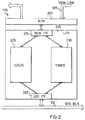
- the remote bridge 125 of a generic node Ni includes a physical interface (PITF) 205 with the remote ring 105.
- the messages transmitted on the remote ring 105 are organized in packets.
- Each packet includes various service fields which identify the destination node, the node which emitted the packet, the length of the packet, the type of packet, its priority for transmission on the remote ring, etc., and a data structure constituted, for example, by 8 blocks (beats) of 64 bits; the packets are defined in accordance with the standard known as the Scalable Coherent Interface (SCI) standard defined in IEEE specification P1596.3/051 (although the use of messages of different types is not excluded).
- SCI Scalable Coherent Interface
- the physical interface 205 receives the packets transmitted on the channel RL(i-1) from the preceding node N(i-1) and determines the corresponding destination node. If the destination node is other than the node Ni, the physical interface 205 transmits the packet received to the next node N(i+1) on the channel RL(i+1). Otherwise, the data structure and the data which identify the type of packet are supplied to a logic interface (LITF) 210 which determines the type of packet and performs the associated operations. Conversely, the logic interface 210 constructs a packet for transmission on the remote ring 105 and supplies it to the physical interface 205 which transmits it to the next node N(i+1) on the channel RL(i+1).
- LITF logic interface
- the logic interface 210 includes a remote interface block (REM ITF) 215 connected to the physical interface 205 and a local interface block (LOC ITF) 220 connected to the system bus 110. Interposed between the remote interface block 215 and the local interface block 220 are a logic block 225 which controls the operation of the remote bridge unit 125 (for example, the coherence protocols of the cache memories), and a timer block 230 which controls the updating and the synchronization of the TBi value.
- REM ITF remote interface block
- LOC ITF local interface block
- timer block is disposed inside the remote bridge unit is particularly advantageous since it enables the TBi values of the various nodes to be synchronized with one another extremely quickly without requiring the transfer of data within the node itself (that is, on the system bus); the present invention may, however, also be implemented with the timer block disposed in a different position, for example, in the arbitration unit, in a processor of the node, or the like.
- the remote interface block 215 decodes the type of packet received from the remote ring 105 (by means of the physical interface 205); if it is a synchronization packet, the corresponding data structure is supplied to the timer block 230, whereas, if not, the data structure is supplied to the logic block 225. Conversely, the remote interface 215 receives a synchronization packet from the timer block 230 or a packet of any other type from the logic block 225 and these are then transmitted to the physical interface 205; a high priority for transmission on the remote ring is preferably associated with the synchronization packets so as to increase the accuracy of the synchronization process.
- the local interface block 220 controls a protocol for access to the system bus 110.
- the local interface 220 receives from the system bus 110 all of the data transmitted thereon; in the case of an instruction which requires an initialization of the TBi value (emitted, for example, by a processor of the node), the corresponding data is supplied to the timer block 230, whereas, otherwise, the data received from the system bus is supplied to the logic block 225.
- the local interface 220 controls requests for access to the system bus 110 in order to transmit thereon data received from the logic block 225 or the system time value received from the timer block 230, in response to a corresponding reading instruction (emitted by any agent of the node).
- the timer block 230 includes a remote input latching block (REM IN) 303 and a remote output latching block (REM OUT) 306 which receive the data structure of the synchronization packet (SYNC DATA) from the remote interface block and transmit it to the remote interface block, respectively.
- REM IN remote input latching block
- REM OUT remote output latching block
- the data structure of the synchronization packet includes an initial field (START), for example, of 64 bits, a final field (END), for example, of 64 bits, and an increment field (INC), for example of 32 bits.
- START initial field
- END final field
- IOC increment field
- the latching block 303 receives the data structure of a synchronization packet as an input and produces the values of the START, END and INC fields at its outputs 303a, 303b and 303c, respectively; conversely, the latching block 306 receives the values of the START, END and INC fields at its inputs 306a, 306b and 306c, and produces the corresponding data structure of a synchronization packet at its output.
- the latching block 306 there is also a register 307 (for example of 16 bits) which stores a NEXTNODE value indicative of the node to which the synchronization packet should be transmitted; this node is preferably set to be the immediately following node (that is, the node physically closest to the node in question).
- a local latching block (LOC IN) 309 receives (from the local interface block) an initialization value (INI) for the TBi value (as a result of a corresponding instruction) and outputs the same value.
- a local output latching block (LOC OUT) 312 outputs a system time equal to the time value TBi in response to a corresponding reading instruction.
- the timing block 230 also includes a register 315 (for example with 64 bits) which stores the TBi value and a register 318 (for example with 16 bits) which stores the LOCPERIODi value.
- the output of the register 315 and the output of the register 318 are connected to the input of an adder circuit (ADD) 321.
- the output of the register 315 and the output of the adder 321 are connected to separate inputs of a multiplexer 324 which transfers to its own output the value present at only one of these inputs, in dependence on a suitable selection signal.
- An adder 325 has an input connected to the output of the register 315 and another input which is kept at a predetermined value, preferably +1.
- a further multiplexer 327 has separate inputs connected to the output of the multiplexer 324, to the output 303a, to the output of the adder 325, and to the output of the latching block 309; the output of the multiplexer 327 is connected to the input of the register 315.
- the output of the register 315 is also connected to the input of the latching block 312.
- a register 336 (for example with 32 bits) is used to store an increment value (INC) indicative of a time required to transmit the synchronization packet from a generic node Ni to a subsequent node N(i+1).
- a comparator circuit 339 has separate inputs connected to the output of the register 315 and to the output 303a. The output of the comparator 339 and the output of the register 336 are connected to the input of an adder 342, the output of which is connected to the input of the register 336.
- a further adder 348 has an input connected to the output 303a and another input connected to the output 303c.
- the output of the adder 345 and the output of the adder 348 are connected to separate inputs of a multiplexer 351 the output of which is connected to the input 306a.
- a register 354 (for example with 32 bits) is used to store the SYNCPERIOD value.
- the output of the register 315 and the output of the register 354 are connected to the input of an adder 357.
- a further adder 360 has an input connected to the output 303b and another input connected to the output 303c.
- a multiplexer 363 has separate inputs connected to the output of the adder 357 and to the output of the adder 360; the output of the multiplexer 363 is connected to the input 306b.
- a multiplexer 364 has separate inputs connected to the output 303c and to the output of the register 336; the multiplexer 364 transfers selectively to its output, which is connected to the input 306c, the value present at only one of these inputs.
- the output of the adder 357 and the output 303b are connected to separate inputs of a multiplexer 366; the output of the multiplexer 366 is connected to the input of a register 369 (for example with 64 bits), used to store a final count value (END).
- a register 369 for example with 64 bits
- END final count value
- the output of the adder 321 and the output of the register 369 are connected to the input of a comparator 372.
- a flag 378 is also used to indicate (for example, when it is turned on) that the node is a master node.
- the operation of the timer block 230 is controlled by a control logic unit (CTRL) 381 constituted basically by a finite state machine, by means of suitable control signals (indicated Sc as a whole).
- CTRL control logic unit
- the output of the comparator 372 and the output of the flag 378 are connected to the input of the logic control unit 381 which also receives as an input a signal REM.STROBE, which indicates (when it is turned on) that the data structure of a synchronization packet is available at the input of the latching block 303, a signal LOC.STROBE, which indicates (when it is turned on) that an initialization value is available at the input of the latching block 309, and a signal READ which indicates (when it is turned on) that the system time has been requested by a reading instruction.
- REM.STROBE which indicates (when it is turned on) that the data structure of a synchronization packet is available at the input of the latching block 303
- LOC.STROBE which indicates (when
- control logic unit 381 is in a state in which, upon each clock signal CLKi, the signal output by the adder 321 is transferred, by means of the multiplexers 324 and 327, to the input of the register 315; the TBi value is thus increased by the LOCPERIODi value upon each clock signal CLKi.
- the control logic unit 381 is brought to a state in which, upon each clock signal CLKi, the signal output by the register 315 is returned to the input of the same register 315 by means of the multiplexers 324 and 327, so as to keep the TBi value fixed.
- the control logic unit 381 controls the structure in a manner such that the signal output by the adder 345 (that is, the sum of the TBi value and the increment value) is transferred, by means of the multiplexer 351, to the input 306a (START field value), the signal output by the adder 357 (that is, the sum of the TBi value and the SYNCPERIOD value) is transferred, by means of the multiplexer 363, to the input 306b (END field value), and the increment value stored in the register 336 is transferred, by means of the multiplexer 364, to the input 306c (INC field value).
- the same signal output by the adder 357 (that is, the sum of the TBi value and the SYNCPERIOD value) is also transferred by the multiplexer 366 to the register 369 (so as to update the final count value) .
- the control logic unit 381 then activates the latching block 306 so as to construct a synchronization packet which contains these values (and the NEXTNODE value) and which is transmitted to the next node on the remote ring.
- the control logic unit 381 activates the latching block 303 in order to obtain the values of the corresponding START, END and INC fields at the outputs 303a, 303b and 303c, respectively.
- the synchronization packet received is suitably modified in order to be transmitted to the next node.
- the signal output by the adder 348 (that is, the sum of the START field value and the INC field value) is transferred, by means of the multiplexer 351, to the input 306a (new START field value)
- the signal output by the adder 360 (that is, the sum of the END field and the INC field values) is transferred, by means of the multiplexer 363, to the input 306b (new END field value)
- the signal at the output 303c (INC field value) is transferred directly by means of the multiplexer 364 to the input 306c (new INC field value).
- the control logic unit 381 then activates the latching block 306 so as to construct a new synchronization packet which contains these values (and the NEXTNODE value) and which is sent to the next node on the remote ring.
- the signal at the output 303a (the START field value) is transferred, by means of the multiplexer 327, to the register 315 (so as to update the TBi value) and the signal at the output 303b (END field value) is transferred, by means of the multiplexer 366, to the register 369 (so as to update the final count value).
- the control logic unit 381 then returns to the normal operating state so that the TBi value is increased by the LOCPERIODi value upon each clock signal.
- the final count values stored in the master node and in the immediately subsequent node are equal.
- the START field value loaded in the register 315 of the next node (equal to the final count TBi value of the master node plus the increment value) will therefore always be greater than the TBi value of the same node (which is kept fixed at the final count value). Similar considerations apply to the other nodes, in which the final count value and the START field value are both increased by the INC field value.
- the control logic unit 381 activates the latching block 303 in order to obtain the START field value of the corresponding data structure at the output 303a.
- This value which is set initially at the TBi value of the master node plus the increment value (INC) and is modified by the addition of the INC field value from every other node, will therefore be equal to the initial TBi value plus N ⁇ INC.
- the START field value received will be equal to the current TBi value; if, on the other hand, the actual transmission time is less than the increment value, the START field value received will be greater than the current TBi value, whereas, if the actual transmission time is greater than the increment value, the START field value received will be less than the current TBi value.
- the START field value received is compared, by means of the comparator 339, with the TBi value stored in the register 315.
- the comparator 339 outputs a signal having a positive value (for example, +1) when the START field value is less than the TBi value, a zero value when the START field value is equal to the TBi value, and a negative value (for example, -1) when the START field value is greater than the TBi value.
- the increment value stored in the register 336 is then consequently modified by the adder circuit 342.
- each node updates its own increment value (indicative of the time taken to transmit the synchronization packet to the next node), or suitable packets are used to determine the transmission time, or the increment value is set at a predetermined value, etc.
- the corresponding LOCPERIODi value is loaded in the register 318 of each node and the register 315 (TBi value) and the register 369 (final count value) are set at the same starting value, for example, zero.
- the master node is set by turning on the corresponding flag 378; at the same time, the SYNCPERIOD value is loaded in the register 354 and the register 336 (increment value) is set at a starting value, for example, zero (these values have no significance in the other nodes).
- the TBi values of all of the nodes are thus immediately equal to the final count values stored in the registers 369 (output signal from the comparator 372 on).
- the TBi value of each non-master node is therefore kept fixed at the same starting value.
- the master node sends a first synchronization packet on the remote ring.
- a non-master node receives this synchronization packet, it updates the TBi value and the final count value and then activates the increment of the TBi value (as described in detail above) .
- the START field value loaded in the register 315 (equal to the starting TBi value of the master node plus the increment value) will always be greater than or at least equal to the TBi value of the node in question (which is kept fixed at the starting value).
- the TBi value (stored in the master node) may also be programmed to an initialization value by means of a corresponding instruction.
- the control logic 381 activates the latching block 309 so that the input signal of the block 309 is transferred to the output thereof and then, by means of the multiplexer 327, to the register 315; the TBi value thus updated is then transmitted to the other nodes of the system with the first synchronization packet, as described above.
- control logic unit 381 transfers the contents of the register 315 (TBi value) to the input of the latching block 312.
- the signal output by the adder 325 is transferred to the input of the register 315, by means of the multiplexer 327, so that the TBi value is increased by 1; the control logic unit 381 then transfers the contents of the register 315 (increased TBi value) to the input of the latching block 312. The signal input to the latching block 312 is then transferred to the output thereof in order to be supplied to the requesting agent.
- the system time output by the latching block 312 when the TBi value is fixed will thus be increased by 1 upon each reading request. This enables the system time never to be stopped (strictly monotonic); moreover, the unitary increment prevents the risk of the TBi value subsequently being less (after a synchronization operation) than the value output at a previous moment.
- the TBi value is increased by a different value (generally of a few units to avoid the risk of having a system time which is not increasing), or reading of the system time is prevented when the TBi value is fixed, etc; the present invention may, however, also be implemented with the output of a system time which is always equal to the TBi value.
Priority Applications (2)
| Application Number | Priority Date | Filing Date | Title |
|---|---|---|---|
| EP19980830417 EP0971282B1 (de) | 1998-07-09 | 1998-07-09 | Mehrprozessorsystem mit synchronisierter Systemzeit |
| DE69833933T DE69833933T2 (de) | 1998-07-09 | 1998-07-09 | Mehrprozessorsystem mit synchronisierter Systemzeit |
Applications Claiming Priority (1)
| Application Number | Priority Date | Filing Date | Title |
|---|---|---|---|
| EP19980830417 EP0971282B1 (de) | 1998-07-09 | 1998-07-09 | Mehrprozessorsystem mit synchronisierter Systemzeit |
Publications (2)
| Publication Number | Publication Date |
|---|---|
| EP0971282A1 true EP0971282A1 (de) | 2000-01-12 |
| EP0971282B1 EP0971282B1 (de) | 2006-03-22 |
Family
ID=8236711
Family Applications (1)
| Application Number | Title | Priority Date | Filing Date |
|---|---|---|---|
| EP19980830417 Expired - Lifetime EP0971282B1 (de) | 1998-07-09 | 1998-07-09 | Mehrprozessorsystem mit synchronisierter Systemzeit |
Country Status (2)
| Country | Link |
|---|---|
| EP (1) | EP0971282B1 (de) |
| DE (1) | DE69833933T2 (de) |
Cited By (2)
| Publication number | Priority date | Publication date | Assignee | Title |
|---|---|---|---|---|
| WO2001090910A2 (en) * | 2000-05-25 | 2001-11-29 | International Business Machines Corporation | Switched-based time synchronization protocol for a numa system |
| EP1671231B1 (de) * | 2003-09-23 | 2019-11-06 | Symantec Operating Corporation | Systeme und verfahren zur zeitabhängigen datenspeicherung und -wiederherstellung |
Citations (3)
| Publication number | Priority date | Publication date | Assignee | Title |
|---|---|---|---|---|
| US4746920A (en) * | 1986-03-28 | 1988-05-24 | Tandem Computers Incorporated | Method and apparatus for clock management |
| GB2267985A (en) * | 1992-06-19 | 1993-12-22 | Westinghouse Electric Corp | Synchronisation of time-of-day clocks in a distributed processing network system |
| EP0722233A2 (de) * | 1994-12-21 | 1996-07-17 | Hewlett-Packard Company | Synchronisierung in einem Datenkommunikationsnetzwerk |
-
1998
- 1998-07-09 DE DE69833933T patent/DE69833933T2/de not_active Expired - Lifetime
- 1998-07-09 EP EP19980830417 patent/EP0971282B1/de not_active Expired - Lifetime
Patent Citations (3)
| Publication number | Priority date | Publication date | Assignee | Title |
|---|---|---|---|---|
| US4746920A (en) * | 1986-03-28 | 1988-05-24 | Tandem Computers Incorporated | Method and apparatus for clock management |
| GB2267985A (en) * | 1992-06-19 | 1993-12-22 | Westinghouse Electric Corp | Synchronisation of time-of-day clocks in a distributed processing network system |
| EP0722233A2 (de) * | 1994-12-21 | 1996-07-17 | Hewlett-Packard Company | Synchronisierung in einem Datenkommunikationsnetzwerk |
Non-Patent Citations (1)
| Title |
|---|
| ABALI B ET AL: "CLOCK SYNCHRONIZATION ON A MULTICOMPUTER", JOURNAL OF PARALLEL AND DISTRIBUTED COMPUTING, vol. 40, no. 1, 10 January 1997 (1997-01-10), pages 118 - 130, XP000682841, ISSN: 0743-7315 * |
Cited By (4)
| Publication number | Priority date | Publication date | Assignee | Title |
|---|---|---|---|---|
| WO2001090910A2 (en) * | 2000-05-25 | 2001-11-29 | International Business Machines Corporation | Switched-based time synchronization protocol for a numa system |
| WO2001090910A3 (en) * | 2000-05-25 | 2003-01-09 | Ibm | Switched-based time synchronization protocol for a numa system |
| US6687756B1 (en) | 2000-05-25 | 2004-02-03 | International Business Machines Corporation | Switched-based time synchronization protocol for a NUMA system |
| EP1671231B1 (de) * | 2003-09-23 | 2019-11-06 | Symantec Operating Corporation | Systeme und verfahren zur zeitabhängigen datenspeicherung und -wiederherstellung |
Also Published As
| Publication number | Publication date |
|---|---|
| DE69833933D1 (de) | 2006-05-11 |
| EP0971282B1 (de) | 2006-03-22 |
| DE69833933T2 (de) | 2006-09-28 |
Similar Documents
| Publication | Publication Date | Title |
|---|---|---|
| RU2176814C2 (ru) | Схема уменьшения задержки при передаче буферизованных данных между двумя взаимно асинхронными шинами | |
| TWI423036B (zh) | 用以在雙向環型互連結構上選擇一方向以傳輸封包之方法及儲存有多個可執行指令的機器可讀媒體 | |
| RU2110838C1 (ru) | Устройство для оптимизации организации доступа к общей шине во время передачи данных с прямым доступом к памяти | |
| JP4355370B2 (ja) | ネットワークノード同期方法 | |
| JP2002049605A (ja) | タイマ調整システム | |
| US6687756B1 (en) | Switched-based time synchronization protocol for a NUMA system | |
| JP2007058854A (ja) | 時間認識システム | |
| US6591370B1 (en) | Multinode computer system with distributed clock synchronization system | |
| US9319237B2 (en) | Method and device for controlling a bus system and a corresponding bus system | |
| Liu et al. | Parallel probe based dynamic connection setup in TDM NoCs | |
| US5870387A (en) | Method and apparatus for initializing a ring | |
| US20050066062A1 (en) | Method and device for determining time in a bus system and corresponding bus system | |
| US5905869A (en) | Time of century counter synchronization using a SCI interconnect | |
| US6473821B1 (en) | Multiple processor interface, synchronization, and arbitration scheme using time multiplexed shared memory for real time systems | |
| CN1322721C (zh) | 使用总线的预仲裁装置及其方法 | |
| EP0971282B1 (de) | Mehrprozessorsystem mit synchronisierter Systemzeit | |
| EP1179785A1 (de) | Verbindungsbussystem | |
| KR102614429B1 (ko) | 재설정 가능한 시스템 프레임워크 및 서버시각 동기부를 포함하는 에지 디바이스용 시스템 온 모듈 | |
| JPH07200486A (ja) | 情報処理装置 | |
| EP0990993A1 (de) | Ereigniszähler | |
| JP4604794B2 (ja) | ノード間接続装置 | |
| JP7418159B2 (ja) | 情報処理装置 | |
| JP2002073577A (ja) | 分散メモリ型並列計算機における分散処理方法及びコンピュータ可読記録媒体 | |
| US7181292B2 (en) | System control method, control processing system, and control processing apparatus | |
| US20010005870A1 (en) | External bus control system |
Legal Events
| Date | Code | Title | Description |
|---|---|---|---|
| PUAI | Public reference made under article 153(3) epc to a published international application that has entered the european phase |
Free format text: ORIGINAL CODE: 0009012 |
|
| AK | Designated contracting states |
Kind code of ref document: A1 Designated state(s): DE FR GB IT |
|
| AX | Request for extension of the european patent |
Free format text: AL;LT;LV;MK;RO;SI |
|
| 17P | Request for examination filed |
Effective date: 20000710 |
|
| AKX | Designation fees paid |
Free format text: DE FR GB IT |
|
| 17Q | First examination report despatched |
Effective date: 20020819 |
|
| GRAP | Despatch of communication of intention to grant a patent |
Free format text: ORIGINAL CODE: EPIDOSNIGR1 |
|
| GRAS | Grant fee paid |
Free format text: ORIGINAL CODE: EPIDOSNIGR3 |
|
| GRAA | (expected) grant |
Free format text: ORIGINAL CODE: 0009210 |
|
| AK | Designated contracting states |
Kind code of ref document: B1 Designated state(s): DE FR GB IT |
|
| REG | Reference to a national code |
Ref country code: GB Ref legal event code: FG4D |
|
| REF | Corresponds to: |
Ref document number: 69833933 Country of ref document: DE Date of ref document: 20060511 Kind code of ref document: P |
|
| ET | Fr: translation filed | ||
| PLBE | No opposition filed within time limit |
Free format text: ORIGINAL CODE: 0009261 |
|
| STAA | Information on the status of an ep patent application or granted ep patent |
Free format text: STATUS: NO OPPOSITION FILED WITHIN TIME LIMIT |
|
| 26N | No opposition filed |
Effective date: 20061227 |
|
| REG | Reference to a national code |
Ref country code: FR Ref legal event code: PLFP Year of fee payment: 19 |
|
| REG | Reference to a national code |
Ref country code: FR Ref legal event code: PLFP Year of fee payment: 20 |
|
| PGFP | Annual fee paid to national office [announced via postgrant information from national office to epo] |
Ref country code: DE Payment date: 20170831 Year of fee payment: 20 Ref country code: IT Payment date: 20170920 Year of fee payment: 20 Ref country code: GB Payment date: 20170920 Year of fee payment: 20 Ref country code: FR Payment date: 20170920 Year of fee payment: 20 |
|
| REG | Reference to a national code |
Ref country code: DE Ref legal event code: R071 Ref document number: 69833933 Country of ref document: DE |
|
| REG | Reference to a national code |
Ref country code: GB Ref legal event code: PE20 Expiry date: 20180708 |
|
| PG25 | Lapsed in a contracting state [announced via postgrant information from national office to epo] |
Ref country code: GB Free format text: LAPSE BECAUSE OF EXPIRATION OF PROTECTION Effective date: 20180708 |