EP0967662A1 - Quantum well detector with a storage well for photoexited electrons - Google Patents
Quantum well detector with a storage well for photoexited electrons Download PDFInfo
- Publication number
- EP0967662A1 EP0967662A1 EP99401373A EP99401373A EP0967662A1 EP 0967662 A1 EP0967662 A1 EP 0967662A1 EP 99401373 A EP99401373 A EP 99401373A EP 99401373 A EP99401373 A EP 99401373A EP 0967662 A1 EP0967662 A1 EP 0967662A1
- Authority
- EP
- European Patent Office
- Prior art keywords
- quantum well
- barrier layer
- layer
- storage layer
- electrons
- Prior art date
- Legal status (The legal status is an assumption and is not a legal conclusion. Google has not performed a legal analysis and makes no representation as to the accuracy of the status listed.)
- Granted
Links
- 239000004065 semiconductor Substances 0.000 claims abstract description 35
- 238000005259 measurement Methods 0.000 claims abstract description 11
- 238000010521 absorption reaction Methods 0.000 claims abstract description 10
- 230000003247 decreasing effect Effects 0.000 claims abstract description 6
- 230000004888 barrier function Effects 0.000 claims description 61
- 239000000463 material Substances 0.000 claims description 27
- 239000000758 substrate Substances 0.000 claims description 9
- 229910045601 alloy Inorganic materials 0.000 claims description 6
- 239000000956 alloy Substances 0.000 claims description 6
- 230000005684 electric field Effects 0.000 claims description 5
- 239000000203 mixture Substances 0.000 claims description 4
- 238000005530 etching Methods 0.000 claims 1
- 239000000969 carrier Substances 0.000 abstract description 11
- 230000006798 recombination Effects 0.000 abstract description 7
- 238000005215 recombination Methods 0.000 abstract description 7
- 238000000034 method Methods 0.000 abstract description 6
- 238000001514 detection method Methods 0.000 abstract description 5
- 238000009825 accumulation Methods 0.000 abstract 5
- 238000005036 potential barrier Methods 0.000 abstract 4
- 230000005284 excitation Effects 0.000 abstract 1
- 229910001218 Gallium arsenide Inorganic materials 0.000 description 20
- 230000002745 absorbent Effects 0.000 description 9
- 239000002250 absorbent Substances 0.000 description 9
- 230000000694 effects Effects 0.000 description 8
- 238000005286 illumination Methods 0.000 description 5
- 230000010354 integration Effects 0.000 description 4
- 230000007704 transition Effects 0.000 description 4
- 230000008901 benefit Effects 0.000 description 3
- 230000004907 flux Effects 0.000 description 3
- 230000004048 modification Effects 0.000 description 3
- 238000012986 modification Methods 0.000 description 3
- 230000003287 optical effect Effects 0.000 description 3
- 238000010586 diagram Methods 0.000 description 2
- 238000009792 diffusion process Methods 0.000 description 2
- 229910000967 As alloy Inorganic materials 0.000 description 1
- 238000004364 calculation method Methods 0.000 description 1
- 230000007423 decrease Effects 0.000 description 1
- 239000002019 doping agent Substances 0.000 description 1
- 230000005274 electronic transitions Effects 0.000 description 1
- 238000005516 engineering process Methods 0.000 description 1
- 230000005281 excited state Effects 0.000 description 1
- 230000001747 exhibiting effect Effects 0.000 description 1
- 238000003384 imaging method Methods 0.000 description 1
- 230000010287 polarization Effects 0.000 description 1
- 235000020004 porter Nutrition 0.000 description 1
- 238000005381 potential energy Methods 0.000 description 1
- 102000012498 secondary active transmembrane transporter activity proteins Human genes 0.000 description 1
- 108040003878 secondary active transmembrane transporter activity proteins Proteins 0.000 description 1
- 230000003595 spectral effect Effects 0.000 description 1
Images


Classifications
-
- H—ELECTRICITY
- H01—ELECTRIC ELEMENTS
- H01L—SEMICONDUCTOR DEVICES NOT COVERED BY CLASS H10
- H01L31/00—Semiconductor devices sensitive to infrared radiation, light, electromagnetic radiation of shorter wavelength or corpuscular radiation and specially adapted either for the conversion of the energy of such radiation into electrical energy or for the control of electrical energy by such radiation; Processes or apparatus specially adapted for the manufacture or treatment thereof or of parts thereof; Details thereof
- H01L31/0248—Semiconductor devices sensitive to infrared radiation, light, electromagnetic radiation of shorter wavelength or corpuscular radiation and specially adapted either for the conversion of the energy of such radiation into electrical energy or for the control of electrical energy by such radiation; Processes or apparatus specially adapted for the manufacture or treatment thereof or of parts thereof; Details thereof characterised by their semiconductor bodies
- H01L31/0352—Semiconductor devices sensitive to infrared radiation, light, electromagnetic radiation of shorter wavelength or corpuscular radiation and specially adapted either for the conversion of the energy of such radiation into electrical energy or for the control of electrical energy by such radiation; Processes or apparatus specially adapted for the manufacture or treatment thereof or of parts thereof; Details thereof characterised by their semiconductor bodies characterised by their shape or by the shapes, relative sizes or disposition of the semiconductor regions
Definitions
- the field of the invention is that of wave detectors electromagnetic made with III-V semiconductor materials from so as to define quantum well structures.
- FIG. 1a gives an example of this type of transition in a well having two discrete levels of energy allowed for the electrons.
- the application of an electric field to this type of configuration makes it possible to extract the electrons located on the second quantum level preferentially.
- the collection in the external electrical circuit of these electrons coming from the second quantum level on which they were carried by an h ⁇ illumination allows the detection of the latter.
- Figure 1b illustrates such a configuration with multiple wells.
- this limitation is due to a layer barrier of too small thickness, between the two neighboring wells constituting the photovoltaic structure.
- the invention proposes to introduce into the detector, a storage layer different from the absorbent layer (quantum well) using a transfer barrier of large width compared to that of the well quantum.
- the transfer barrier has a potential profile conduction, decreasing from the quantum well.
- the invention relates to a wave detector electromagnetic including a stack of layers of materials III-V semiconductors, the conduction band profile of said materials defining at least one quantum well, said quantum well having at minus a first discrete level of energy populated by electrons capable of go to a second energy level under the absorption of a wave electromagnetic and means for reading said electrons in the second energy level characterized in that the stack of layers in semiconductor material further includes a storage layer of electrons separated from the quantum well, by a barrier layer of transfer, the thickness of the transfer barrier layer being approximately one order of magnitude greater than the thickness of the quantum well, the level lower energy of the conduction band of the barrier layer transfer being greater than those of the quantum well and the layer of electron storage and decreasing from the quantum well to the electron storage layer so as to promote the flow of electrons from the second energy state into the layer of electron storage.
- the transfer barrier can be composed of a semiconductor alloy whose composition varies along the thickness of said barrier so that the potential for conduction decreases as one moves away from the well.
- the transfer barrier can be produced with a piezoelectric material which generates a field natural electric, allowing the conduction potential of the transfer barrier, the required profile.
- the structure semiconductor can also be put directly under field electric to obtain the desired conduction potential profile, for the transfer barrier.
- the reading of the photodetection signal can be performed in different ways.
- Figure 3 illustrates the profile of conduction bands of the aforementioned layer stack
- the transfer barrier being very thick, the electrons being captured in the storage layer stay there very long (from a few ⁇ s to a few ms).
- the return to balance of carriers in the quantum well by tunnel effect is indeed very long across the barrier of very thick transfer (you can choose a thickness of several hundreds of nanometers if desired).
- the photoconductivity gain is so very high if we compare this time to the lifetime of the electrons photoexcited in conventional quantum well detectors (of the order of the ps).
- first and second ohmic contacts contact the storage layer without contacting the absorbing quantum well as illustrated in FIG. 4, which takes up the stack of layers of semiconductor materials illustrated in FIG. 2, and which shows the ohmic contacts C 1 and C 2 .
- the arrows illustrate the path of the electrons and their flow from the quantum well 3 to the storage layer 5 in which they are collected thanks to the contacts C 1 and C 2 .
- This photocurrent is proportional to the number of electrons captured, and the time to read it is very long if we compare with conventional quantum well detectors.
- the storage layer being undoped, the current is very weak without illuminating the structure since this layer contains very few carriers at thermodynamic equilibrium.
- the illumination of the structure sends electrons to the excited level E 2 of the absorbing quantum well, part of these transit to the storage layer via the transfer barrier.
- the conductivity of the storage layer then increases enormously.
- the storage layer is the channel, the role of the gate is played by the optical beam to be detected, and the source and the drain are the two electrodes between which the photocurrent is read.
- the ohmic contacts do not reach the absorbent well. It is known by diffusion of dopants to make contacts which reach the storage layer without touching the absorbent well for a transfer barrier separating the two layers as fine as 500 ⁇ .
- Another contact geometry consists in carrying out a mesa by a completely standard technology, and then come to contact the layer of storage below the quantum well. In this case, during growth, the order of the layers has been reversed compared to the previous solution. This solution has the advantage of not requiring control of the depth of the contact.
- the diagram is shown in Figure 5; the transistor function optically controlled appears more clearly.
- R electrical resistance
- ⁇ 10 5 cm2V -1 s -1 , which is common for GaAs transistor channels at 77K.
- This very low resistance therefore corresponds to a photocurrent of 40 ⁇ A for a polarization of 1 mV between the source and the drain.
- These photocurrents are much higher than the photocurrents of the usual quantum well detectors, due to the increase in the gain of photoconductivity.
- the voltage due to the spacing between the electrons in the storage layer and the absorbent well layer, which is doped, is measured by two ohmic contacts taken respectively at the storage layer (contact C ' 1 ) and at the quantum well (contact C' 2 ) as illustrated in Figure 7.
- the voltage is read directly, which will be between 0 and 180 mV in the case of a barrier whose percentage of Al varies from 30% to 8% in an Al x Ga 1-x As alloy. Note that the maximum value of the voltage does not depend on the width of the storage layer. The effect of this width is above all the modification of the time of return to equilibrium of the electrons.
- This type of detector will therefore be particularly well suited to the detection in a spectral area where there are few photons, like the area 3-5 ⁇ m for infrared black body imaging at 300 K.
- a perpendicular tension can be applied to the device to force the electrons back into the well absorbing quantum if you want to initialize the system between two measurements.
- This initialization principle can be used during reading to set the desired level of the number of electrons in the storage layer. This allows for example to adjust the potential energy in the layer of storage with an offset such that the electron population is low under a enlightenment given. Thanks to this offset, the detector only links variations of illumination compared to the average level of illumination, which is very interesting when the detector analyzes a mid-infrared scene at ambient temperature.
- absorption to detect the electrons located on the energy level E 1 pass on the energy level E 2 to be then evacuated via the transfer barrier, in the storage layer, in which they can accumulate.
- the quantum well has a second discrete level of energy E 2 . It is also possible to use a structure in which the quantum well comprises only one discrete level of energy. The optical transition can then take place between the energy level E 1 and the continuum of levels above the barrier as is known in the prior art.
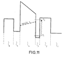
- This example of stacking of semiconductor materials comprises a material constituting the transfer barrier composed of an alloy whose composition varies and in which the transport of electrons can be carried out via the valleys X as illustrated in FIG. 11.
- This type of behavior is obtained in particular with an alloy of Al x Ga 1-x As, for which the percentage x increases from 0.44 to 1.
- the level of the valleys X in the material drops by about 320 meV in the material Al 0.5 Ga 0.5 As at around 200 meV in the AlAs material, relative to the bottom of the conduction band.
- the substrate, the quantum well stop layers and the storage layer can be identical to those of Example 1.
Landscapes
- Physics & Mathematics (AREA)
- Condensed Matter Physics & Semiconductors (AREA)
- Electromagnetism (AREA)
- General Physics & Mathematics (AREA)
- Engineering & Computer Science (AREA)
- Computer Hardware Design (AREA)
- Microelectronics & Electronic Packaging (AREA)
- Power Engineering (AREA)
- Light Receiving Elements (AREA)
Abstract
Description
Le domaine de l'invention est celui des détecteurs d'onde électromagnétique réalisés avec des matériaux semiconducteurs III-V de manière à définir des structures à puits quantiques.The field of the invention is that of wave detectors electromagnetic made with III-V semiconductor materials from so as to define quantum well structures.
Le fonctionnement de tels détecteurs est basé sur l'occurrence de transitions électroniques entre niveaux permis d'énergie (e1 et e2) au sein de la bande de conduction de structures quantiques semiconductrices. La figure 1a donne un exemple de ce type de transition dans un puits présentant deux niveaux discrets d'énergie permise pour les électrons. L'application d'un champ électrique à ce type de configuration permet d'extraire du puits de manière préférentielle les électrons situés sur le deuxième niveau quantique. Ainsi, la collection dans le circuit électrique extérieur de ces électrons provenant du deuxième niveau quantique sur lequel ils ont été portés par un éclairement hν, permet la détection de ce dernier.The operation of such detectors is based on the occurrence of electronic transitions between permitted energy levels (e 1 and e 2 ) within the conduction band of semiconductor quantum structures. FIG. 1a gives an example of this type of transition in a well having two discrete levels of energy allowed for the electrons. The application of an electric field to this type of configuration makes it possible to extract the electrons located on the second quantum level preferentially. Thus, the collection in the external electrical circuit of these electrons coming from the second quantum level on which they were carried by an hν illumination, allows the detection of the latter.
Pour obtenir une absorption importante de l'éclairement à détecter, on peut utiliser un grand nombre de puits au sein des détecteurs basés sur ce principe quantique. La figure 1b illustre une telle configuration à puits multiples.To obtain a significant absorption of the illumination at detect, you can use a large number of wells within the detectors based on this quantum principle. Figure 1b illustrates such a configuration with multiple wells.
Le problème rencontré avec les structures de l'art antérieur, décrites ci-dessus, réside dans le taux important de recombinaison de porteurs, notamment du à une couche barrière entre puits successifs, de faible épaisseur, voisine de celle des puits quantiques.The problem encountered with the structures of the prior art, described above, lies in the high rate of recombination of carriers, in particular due to a barrier layer between successive wells, of thin, close to that of quantum wells.
Des variantes photovoltaïques de ces détecteurs ont été proposées dans la littérature [Borge VINTER « Detectivity of a three level quantum well detector », IEEE Journal of Quantum Electronics, Vol 30, p. 115 (1994)].Photovoltaic variants of these detectors have been proposed in the literature [Borge VINTER “Detectivity of a three level quantum well detector ”, IEEE Journal of Quantum Electronics, Vol 30, p. 115 (1994)].
Le problème rencontré avec des structures de l'art antérieur, décrites ci-dessus, réside dans le taux important de recombinaison de porteurs.The problem encountered with structures of the prior art, described above, lies in the high rate of recombination of carriers.
Cette recombinaison limite les performances de ces détecteurs et en particulier leur température de fonctionnement. This recombination limits the performance of these detectors and in particular their operating temperature.
Dans le cas photovoltaïque, cette limitation est due à une couche barrière de trop faible épaisseur, entre les deux puits voisins constituant la structure photovoltaïque.In the photovoltaic case, this limitation is due to a layer barrier of too small thickness, between the two neighboring wells constituting the photovoltaic structure.
Pour limiter notablement le taux de recombinaison des porteurs, l'invention propose d'introduire dans le détecteur, une couche de stockage différente de la couche absorbante (puits quantique) et ce à l'aide d'une barrière de transfert de largeur importante par rapport à celle du puits quantique. En séparant ainsi la fonction d'absorption (dans le puits quantique) et la fonction de lecture des photoporteurs (dans une couche de stockage), on améliore les performances des détecteurs en évitant les recombinaisons de porteurs.To notably limit the rate of recombination of carriers, the invention proposes to introduce into the detector, a storage layer different from the absorbent layer (quantum well) using a transfer barrier of large width compared to that of the well quantum. By thus separating the absorption function (in the well quantum) and the reading function of photocarriers (in a layer of storage), the performance of the detectors is improved by avoiding carrier recombinations.
Pour permettre l'écoulement des électrons photoexcités dans la couche de stockage, la barrière de transfert présente un profil de potentiel de conduction, décroissant à partir du puits quantique.To allow the flow of photoexcited electrons in the storage layer, the transfer barrier has a potential profile conduction, decreasing from the quantum well.
Plus précisément, l'invention a pour objet un détecteur d'ondes électromagnétiques comprenant un empilement de couches en matériaux semiconducteurs III-V, le profil de bande de conduction desdits matériaux définissant au moins un puits quantique, ledit puits quantique présentant au moins un premier niveau discret d'énergie peuplé d'électrons capables de passer à un second niveau d'énergie sous l'absorption d'une onde électromagnétique et des moyens de lecture desdits électrons dans le second niveau d'énergie caractérisé en ce que l'empilement de couches en matériaux semiconducteurs comprend en outre, une couche de stockage d'électrons séparée du puits quantique, par une couche barrière de transfert, l'épaisseur de la couche barrière de transfert étant environ d'un ordre de grandeur supérieur à l'épaisseur du puits quantique, le niveau énergétique inférieur de la bande de conduction de la couche barrière de transfert étant supérieur à ceux du puits quantique et de la couche de stockage d'électrons et décroissante depuis le puits quantique jusqu'à la couche de stockage d'électrons de manière à favoriser l'écoulement des électrons depuis le second état d'énergie jusque dans la couche de stockage d'électrons.More specifically, the invention relates to a wave detector electromagnetic including a stack of layers of materials III-V semiconductors, the conduction band profile of said materials defining at least one quantum well, said quantum well having at minus a first discrete level of energy populated by electrons capable of go to a second energy level under the absorption of a wave electromagnetic and means for reading said electrons in the second energy level characterized in that the stack of layers in semiconductor material further includes a storage layer of electrons separated from the quantum well, by a barrier layer of transfer, the thickness of the transfer barrier layer being approximately one order of magnitude greater than the thickness of the quantum well, the level lower energy of the conduction band of the barrier layer transfer being greater than those of the quantum well and the layer of electron storage and decreasing from the quantum well to the electron storage layer so as to promote the flow of electrons from the second energy state into the layer of electron storage.
Ainsi le détecteur de l'invention comprend :
- un puits quantique présentant une absorption intersousbande à l'énergie désirée, cette couche étant tout à fait similaire aux puits quantiques utilisés habituellement dans les détecteurs à puits quantiques [B. Levine « Quantum Well lnfrared Photodetectors », Journal of Applied Physics, volume 74, n° 8, R1. (1993)];
- une barrière de transfert qui se comporte comme une perte de potentiel dans laquelle les électrons photoexcités peuvent être transférés ;
- une couche de stockage des électrons photoexcités ;
- des moyens de lecture du photosignal.
- a quantum well exhibiting an intersubband absorption at the desired energy, this layer being quite similar to the quantum wells usually used in quantum well detectors [B. Levine "Quantum Well lnfrared Photodetectors", Journal of Applied Physics, volume 74, n ° 8, R1. (1993)];
- a transfer barrier which behaves like a loss of potential into which the photoexcited electrons can be transferred;
- a photoexcited electron storage layer;
- means of reading the photosignal.
Selon une première variante de l'invention, la barrière de transfert peut être composée d'un alliage semiconducteur dont la composition varie le long de l'épaisseur de ladite barrière de manière à ce que le potentiel de conduction décroisse quand on s'éloigne du puits.According to a first variant of the invention, the transfer barrier can be composed of a semiconductor alloy whose composition varies along the thickness of said barrier so that the potential for conduction decreases as one moves away from the well.
Selon une seconde variante de l'invention, la barrière de transfert peut être élaborée avec un matériau piézoélectrique qui génère un champ électrique naturel, permettant de conférer au potentiel de conduction de la barrière de transfert, le profil requis.According to a second variant of the invention, the transfer barrier can be produced with a piezoelectric material which generates a field natural electric, allowing the conduction potential of the transfer barrier, the required profile.
Selon une troisième variante de l'invention, la structure semiconductrice peut également être mise directement sous champ électrique pour obtenir le profil de potentiel de conduction désiré, pour la barrière de transfert.According to a third variant of the invention, the structure semiconductor can also be put directly under field electric to obtain the desired conduction potential profile, for the transfer barrier.
Par ailleurs, la lecture du signal de photodétection peut être effectuée de différente manière.Furthermore, the reading of the photodetection signal can be performed in different ways.
Il peut s'agir notamment d'une mesure de photocourant parallèle, utilisant des contacts ohmiques contactant la couche de stockage sans contacter le puits quantique absorbant.It may especially be a measurement of parallel photocurrent, using ohmic contacts contacting the storage layer without contact the absorbent quantum well.
Il peut également s'agir d'une lecture photovoltaïque de la tension due à l'espacement entre les électrons dans la couche de stockage et la couche du puits absorbant.It can also be a photovoltaic reading of the voltage due to the spacing between the electrons in the storage layer and the absorbent well layer.
L'invention sera mieux comprise et d'autres avantages apparaítront à la lecture de la description qui va suivre, donnée à titre non limitatif et grâce aux figures annexées parmi lesquelles :
- la figure 1a schématise un dispositif de détection d'ondes électromagnétiques comprenant un puits quantique, selon l'art connu;
- la figure 1b schématise une structure multipuits quantiques utilisée dans des dispositifs de détection selon l'art connu ;
- la figure 2 illustre un empilement de couches semiconductrices utilisé dans un détecteur selon l'invention ;
- la figure 3 illustre le profil des bandes de conduction de l'empilement de couches précité ;
- la figure 4 illustre un premier exemple de moyens de lecture des électrons photoexcités dans une mesure de photocourant parallèle dans un détecteur selon l'invention ;
- la figure 5 illustre un second exemple de moyens de lecture des électrons photoexcités dans une mesure de photocourant parallèle dans un détecteur selon l'invention ;
- la figure 6 illustre le profil modifié des bandes de conduction de l'empilement de couches illustré en figure 3, tenant compte des effets de charge d'espace ; la modification de ce profil provenant du transfert d'une population d'électrons du puits quantique vers la couche de stockage ;
- la figure 7 illustre un exemple de moyens de lecture des électrons photoexcités dans une mesure photovoltaïque dans un détecteur selon l'invention ;
- la figure 8 illustre un détecteur selon l'invention comprenant des moyens de lecture dans une mesure de photocourant parallèle et des moyens de remise à zéro du détecteur ;
- la figure 9 illustre un deuxième exemple de profil de bande de conduction utilisé dans un empilement de couches d'un détecteur selon l'invention ;
- la figure 10 illustre un troisième exemple de profil de bande de conduction utilisé dans un empilement de couches d'un détecteur selon l'invention ;
- la figure 11 illustre un quatrième exemple de profil de bande de conduction utilisé dans un empilement de couches d'un détecteur selon l'invention.
- Figure 1a shows schematically an electromagnetic wave detection device comprising a quantum well, according to the known art;
- FIG. 1b schematizes a quantum multi-well structure used in detection devices according to the known art;
- FIG. 2 illustrates a stack of semiconductor layers used in a detector according to the invention;
- FIG. 3 illustrates the profile of the conduction bands of the above-mentioned stack of layers;
- FIG. 4 illustrates a first example of means for reading the photoexcited electrons in a parallel photocurrent measurement in a detector according to the invention;
- FIG. 5 illustrates a second example of means for reading the photoexcited electrons in a parallel photocurrent measurement in a detector according to the invention;
- FIG. 6 illustrates the modified profile of the conduction bands of the stack of layers illustrated in FIG. 3, taking into account the effects of space charge; the modification of this profile resulting from the transfer of an electron population from the quantum well to the storage layer;
- FIG. 7 illustrates an example of means for reading the photoexcited electrons in a photovoltaic measurement in a detector according to the invention;
- FIG. 8 illustrates a detector according to the invention comprising means for reading in a parallel photocurrent measurement and means for resetting the detector to zero;
- FIG. 9 illustrates a second example of a conduction band profile used in a stack of layers of a detector according to the invention;
- FIG. 10 illustrates a third example of a conduction band profile used in a stack of layers of a detector according to the invention;
- FIG. 11 illustrates a fourth example of a conduction band profile used in a stack of layers of a detector according to the invention.
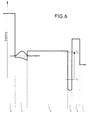
De manière générale, le détecteur selon l'invention comprend un empilement de couches semiconductrices comportant notamment comme l'illustre la figure 2 :
- un
substrat 1 ; - une première couche d'arrêt 2 pour confiner les électrons dans le puits quantique ;
- une couche constitutive du puits quantique 3 ;
- une couche de barrière de transfert à profil de bande de conduction inclinée, 4;
- une couche de stockage d'électrons photoexcités 5 ;
- une deuxième couche d'arrêt 6.
- a
substrate 1; - a
first stop layer 2 for confining the electrons in the quantum well; - a layer constituting the
quantum well 3; - a transfer barrier layer with an inclined conduction band profile, 4;
- a photoexcited
electron storage layer 5; - a
second barrier layer 6.
La figure 3 illustre le profil de bandes de conduction de l'empilement de couche précité ;Figure 3 illustrates the profile of conduction bands of the aforementioned layer stack;
Typiquement, il existe un ordre de grandeur entre la largeur du puits quantique Iq et la largeur de la barrière de transfert Ib, pour éviter les recombinaisons possibles des électrons photoexcités.Typically, there is an order of magnitude between the width of the quantum well I q and the width of the transfer barrier I b , to avoid possible recombinations of the photoexcited electrons.
En effet, la barrière de transfert étant très épaisse, les électrons étant capturés dans la couche de stockage y restent très longtemps (de quelques µs à quelques ms). Le retour à l'équilibre des porteurs dans le puits quantique par effet tunnel est en effet très long à travers la barrière de transfert de grande épaisseur (on peut choisir une épaisseur de plusieurs centaines de nanomètres si on le désire). Le gain de photoconductivité est donc très élevé si l'on compare ce temps à la durée de vie des électrons photoexcités dans les détecteurs à puits quantiques classiques (de l'ordre de la ps).Indeed, the transfer barrier being very thick, the electrons being captured in the storage layer stay there very long (from a few µs to a few ms). The return to balance of carriers in the quantum well by tunnel effect is indeed very long across the barrier of very thick transfer (you can choose a thickness of several hundreds of nanometers if desired). The photoconductivity gain is so very high if we compare this time to the lifetime of the electrons photoexcited in conventional quantum well detectors (of the order of the ps).
Pour effectuer la lecture du signal de photodétection, il est possible d'utiliser deux méthodes que nous allons décrire ci-après.To read the photodetection signal, it is possible to use two methods which we will describe below.
Cette mesure est effectuée dans le plan de la couche de stockage
d'électrons. Pour cela, des premier et second contacts ohmiques contactent
la couche de stockage sans contacter le puits quantique absorbant comme
l'illustre la figure 4, qui reprend l'empilement de couches de matériaux
semiconducteurs illustré en figure 2, et qui fait figurer les contacts ohmiques
C1 et C2. Les flèches illustrent le cheminement des électrons et leur
écoulement depuis le puits quantique 3 jusque dans la couche de stockage
5 dans laquelle ils sont collectés grâce aux contacts C1 et C2. Ceci suppose
que l'épaisseur de la barrière de transfert est suffisamment grande pour que
la diffusion du contact ohmique contacte la couche de stockage sans
atteindre le puits quantique absorbant. Ce photocourant est proportionnel au
nombre d'électrons capturés, et le temps pour le lire est très long si l'on
compare avec les détecteurs à puits quantiques classiques. La couche de
stockage étant non dopée, le courant est très faible sans éclairement de la
structure puisque cette couche contient très peu de porteurs à l'équilibre
thermodynamique. L'éclairement de la structure envoie des électrons sur le
niveau excité E2 du puits quantique absorbant, une partie de ceux-ci
transitent vers la couche de stockage via la barrière de transfert. La
conductivité de la couche de stockage s'accroít alors énormément. On a
donc conceptuellement un transistor contrôlé optiquement : La couche de
stockage est le canal, le rôle de la grille est joué par le faisceau optique à
détecter, et la source et le drain sont les deux électrodes entre lesquelles
est lu le photocourant. Il faut ici insister sur l'importance capitale que les
contacts ohmiques n'atteignent pas le puits absorbant. On sait par diffusion
de dopants faire des contacts qui atteignent la couche de stockage sans
toucher au puits absorbant pour une barrière de transfert séparant les deux
couches aussi fine que 500Å.This measurement is made in the plane of the electron storage layer. For this, first and second ohmic contacts contact the storage layer without contacting the absorbing quantum well as illustrated in FIG. 4, which takes up the stack of layers of semiconductor materials illustrated in FIG. 2, and which shows the ohmic contacts C 1 and C 2 . The arrows illustrate the path of the electrons and their flow from the quantum well 3 to the
Une autre géométrie de contacts consiste à réaliser une mesa par une technologie tout à fait standard, et venir ensuite contacter la couche de stockage en dessous du puits quantique. Dans ce cas, lors de la croissance, l'ordre des couches a été inversé par rapport à la solution précédente. Cette solution a l'avantage de ne pas nécessiter la maítrise de la profondeur du contact. Le schéma est représenté à la figure 5 ; la fonction de transistor contrôlé optiquement apparaít plus clairement.Another contact geometry consists in carrying out a mesa by a completely standard technology, and then come to contact the layer of storage below the quantum well. In this case, during growth, the order of the layers has been reversed compared to the previous solution. This solution has the advantage of not requiring control of the depth of the contact. The diagram is shown in Figure 5; the transistor function optically controlled appears more clearly.
Avec un flux typique de 1016 photons.cm-2.s-1, et une absorption
de 5% dans le puits quantique unique (chiffre courant pour un puits
quantique muni d'un réseau de diffraction en surface), on a placé sur le
niveau E2 (état excité) environ 5.1014 électrons/cm-2 et par seconde. Si l'on
suppose une probabilité 1/2 pour un électron de partir dans la barrière de
transfert pour atteindre la couche de stockage (contre une probabilité 1/2 de
retomber sur le niveau fondamental du puits et donc de ne servir à rien pour
la photodétection), cela mène, pendant 10ms de temps d'intégration, à
2.5.1012cm-2 électrons transférés dans la couche de stockage.With a typical flux of 10 16 photons.cm -2 .s -1 , and an absorption of 5% in the single quantum well (current figure for a quantum well provided with a diffraction grating on the surface), we placed on the level E 2 (excited state) about 5.10 14 electrons / cm -2 and per second. If we assume a
En réalité ce modèle est trop simpliste et il nous faut absolument tenir compte des effets de charge d'espace dans cette structure où les électrons sont transférés loin des atomes dopants. Les effets de charge d'espace mènent à un champ induit dans la barrière de transfert, et celle-ci cessera de transférer les porteurs quand ce champ induit compensera la pente de potentiel existant naturellement dans la barrière de transfert. A cause de ces effets de charge d'espace, la structure de bande est déformée et passe de celle représentée figure 3 à celle représentée figure 6.In reality this model is too simplistic and we absolutely need take into account the space charge effects in this structure where the electrons are transferred away from doping atoms. Load effects of space lead to an induced field in the transfer barrier, and this one will cease to transfer carriers when this induced field compensates for the potential slope naturally existing in the transfer barrier. AT because of these space charge effects, the band structure is deformed and passes from that shown in Figure 3 to that shown in Figure 6.
Pour calculer le nombre maximum de porteurs transférables dans la couche de stockage, on écrit l'équilibre entre le champ dû aux effets de charge d'espace et le pente de potentiel dans la barrière de transfert, sans porteurs transférés. Pour une barrière comme celle de la figure 2, cela mène à une pente de potentiel égale à 180meV/500Å=36kV/cm.To calculate the maximum number of transferable carriers in the storage layer, we write the balance between the field due to the effects of space charge and potential slope in the transfer barrier, without porters transferred. For a barrier like the one in Figure 2, this leads at a potential slope equal to 180meV / 500Å = 36kV / cm.
Le champ dû aux effets de charge d'espace est égal à E = ρS e / ε0εr, où ρS est la densité d'électrons transférés. En égalant les deux quantités, on déduit que ρs est de l'ordre de 2.5 1011 cm-2.The field due to space charge effects is equal to E = ρ S e / ε 0 ε r , where ρ S is the density of transferred electrons. By equalizing the two quantities, we deduce that ρ s is of the order of 2.5 10 11 cm -2 .
Compte tenu des calculs précédents, on voit que la couche de stockage a été remplie au bout d'un temps d'intégration d'environ 500µs pour les niveaux d'éclairements donnés ci-dessus.Given the previous calculations, we see that the layer of storage was filled after an integration time of around 500µs for the lighting levels given above.
La couche de stockage présente alors une résistance électrique (pour une surface standard de pixel utilisé dans les détecteurs, égale à 30µm*30µm) de R = L/NqµS = 250 Ω. Pour cela on a pris une mobilité de µ=105 cm2V-1s-1, ce qui est courant pour des canaux de transistor en GaAs à 77K. Cette résistance, très faible, correspond donc à un photocourant de 40µA pour une polarisation de 1mV entre la source et le drain. Ces photocourants sont largement supérieurs aux photocourants des détecteurs à puits quantiques habituels, en raison de l'augmentation du gain de photoconductivité. The storage layer then has an electrical resistance (for a standard pixel surface used in the detectors, equal to 30 μm * 30 μm) of R = L / NqµS = 250 Ω. For this we took a mobility of µ = 10 5 cm2V -1 s -1 , which is common for GaAs transistor channels at 77K. This very low resistance therefore corresponds to a photocurrent of 40 μA for a polarization of 1 mV between the source and the drain. These photocurrents are much higher than the photocurrents of the usual quantum well detectors, due to the increase in the gain of photoconductivity.
Dans ce cas, on mesure la tension due à l'espacement entre les électrons dans la couche de stockage et la couche du puits absorbant, qui est dopé et ce grâce à deux contacts ohmiques pris respectivement au niveau de la couche de stockage (contact C'1) et au niveau du puits quantique (contact C'2) comme l'illustre la figure 7. On lit directement la tension, qui sera comprise entre 0 et 180 mV dans le cas d'une barrière dont le pourcentage d'Al varie de 30% à 8% dans un alliage AlxGa1-xAs. Il faut noter que la valeur maximale de la tension ne dépend pas de la largeur de la couche de stockage. L'effet de cette largeur est surtout la modification du temps de retour à l'équilibre des électrons.In this case, the voltage due to the spacing between the electrons in the storage layer and the absorbent well layer, which is doped, is measured by two ohmic contacts taken respectively at the storage layer (contact C ' 1 ) and at the quantum well (contact C' 2 ) as illustrated in Figure 7. The voltage is read directly, which will be between 0 and 180 mV in the case of a barrier whose percentage of Al varies from 30% to 8% in an Al x Ga 1-x As alloy. Note that the maximum value of the voltage does not depend on the width of the storage layer. The effect of this width is above all the modification of the time of return to equilibrium of the electrons.
On mesurera la tension maximale de 180 mV (c'est à dire qu'on sera à saturation) pour un flux typique de 1016 photons.cm- 2 pendant un temps d'intégration de 500µs environ. Un temps d'intégration de 30ms permet d'obtenir une tension de 180mV pour un flux de photons très faible : 2.1014 photons.cm- 2 seulement.We will measure the maximum voltage of 180 mV (that is, we will be at saturation) for a typical flux of 10 16 photons.cm- 2 during an integration time of approximately 500 μs. An integration time of 30 ms makes it possible to obtain a voltage of 180 mV for a very low photon flux: 2.10 14 photons.cm- 2 only.
Ce type de détecteur sera donc particulièrement bien adapté à la détection dans une zone spectrale où il y a peu de photons, comme la zone 3-5 µm pour l'imagerie infrarouge de corps noirs à 300 K.This type of detector will therefore be particularly well suited to the detection in a spectral area where there are few photons, like the area 3-5 µm for infrared black body imaging at 300 K.
La détectivité supérieure de ce type de détecteur photovoltaïque
par rapport au détecteurs photovoltaïques à puits quantiques décrits
précédemment dans la littérature [B. Vinter, « Detectivity of a three-level
quantum well detector », IEEE J. of Quantum Electronics, Vol. 30, p. 115
(1994)] provient de deux avantages spécifiques.
Dans tous les cas, une tension perpendiculaire peut être appliquée au dispositif pour forcer les électrons à revenir dans le puits quantique absorbant si l'on désire initialiser le système entre deux mesures.In any case, a perpendicular tension can be applied to the device to force the electrons back into the well absorbing quantum if you want to initialize the system between two measurements.
Dans le cas de la première méthode de lecture photoconductive, il faut rajouter deux couches dopées n+, 1' et 6' au niveau de l'empilement des couches (2 → 6) illustré en figures 4, 5 et 7, une sur le dessus et une autre en dessous de la structure. On obtient alors un dispositif a quatre contacts C1, C2, C3, C4 comme illustré en figure 8In the case of the first photoconductive reading method, two n + doped layers, 1 'and 6' must be added at the stack of layers (2 → 6) illustrated in Figures 4, 5 and 7, one on top and another below the structure. A device with four contacts C 1 , C 2 , C 3 , C 4 is then obtained as illustrated in FIG. 8
Dans le cas de la seconde méthode de lecture photovoltaïque, on peut rester avec le schéma de la figure 7, et on garde deux contacts seulement. On se sert des deux contacts pour la lecture de la tension et pour l'initialisation du système.In the case of the second photovoltaic reading method, we can stay with the diagram of figure 7, and we keep two contacts only. We use the two contacts to read the voltage and for system initialization.
Ce principe d'initialisation peut être utilisé pendant la lecture pour régler le niveau désiré du nombre d'électrons dans la couche de stockage. Cela permet par exemple de régler l'énergie potentielle dans la couche de stockage avec un offset tel que la population d'électrons est faible sous un éclairement donné. Grâce à cet offset, le détecteur ne lie que les variations d'éclairement par rapport au niveau moyen d'éclairement, ce qui est très intéressant quand le détecteur analyse une scène infrarouge moyen à température ambiante.This initialization principle can be used during reading to set the desired level of the number of electrons in the storage layer. This allows for example to adjust the potential energy in the layer of storage with an offset such that the electron population is low under a enlightenment given. Thanks to this offset, the detector only links variations of illumination compared to the average level of illumination, which is very interesting when the detector analyzes a mid-infrared scene at ambient temperature.
Signalons qu'un certain nombre de possibilités peuvent être utilisées avec les détecteurs décrits ici, elles n'ont pas été décrites car elles ne sont pas caractéristiques de l'invention. Citons simplement les réseaux de diffraction gravés sur le dessus du détecteur pour coupler la lumière incidente à la transition intersousbande du puits absorbant et obtenir ainsi une absorption maximale (ceci est très classique dans la littérature).Note that a number of possibilities can be used with the detectors described here, they have not been described because they are not characteristic of the invention. Let's just mention the networks diffraction plates etched on top of the detector to couple the light incident at the intersubband transition of the absorbent well and thus obtain maximum absorption (this is very classic in the literature).
Nous allons décrire plus en détail des exemples de structures d'empilement pouvant être utilisées dans des détecteurs selon l'invention.We will describe in more detail examples of structures which can be used in detectors according to the invention.
Premier exemple d'empilement de couches semiconductrices pouvant être utilisé dans l'invention, dont le profil de bande de conduction correspond à celui illustré en figure 3. First example of stacking of semiconductor layers can be used in the invention, including the conduction band profile corresponds to that illustrated in Figure 3.
Il s'agit d'une configuration dans laquelle la barrière de transfert est constituée d'un alliage dont la composition varie le long de l'épaisseur pour obtenir le profil désiré au niveau du potentiel de conduction de la barrière de transfert.This is a configuration in which the transfer barrier consists of an alloy whose composition varies along the thickness to obtain the desired profile at the conduction potential of the transfer barrier.
Selon cet exemple :
- le substrat 1 est en GaAs, par exemple non dopé ;
- la couche d'arrêt 2 est en Al0,44Ga0,56As, d'épaisseur 300 Å;
- le puits quantique présentant deux niveaux discrets d'énergie E1 et E2 est en In0,15Ga0,85As et typiquement une épaisseur lq = 30 Å ;
- la barrière de transfert est réalisée avec l'alliage AlyGa1-yAs d'épaisseur 500 Å, le pourcentage y variant linéairement de 0,3 à 0,08, à partir du puits quantique permettant d'obtenir une chute de potentiel variant de 250 meV à 70 meV par rapport au bas de la bande de conduction de GaAs ;
- la couche de stockage 5 est réalisée avec du GaAs et présente une épaisseur de 150 Å;
la couche 6 est en Al0,44Ga0,56As identique à la première couche d'arrêt 2.
- the
substrate 1 is made of GaAs, for example undoped; - the
barrier layer 2 is made of Al 0.44 Ga 0.56 As, 300 Å thick; - the quantum well having two discrete energy levels E 1 and E 2 is in In 0.15 Ga 0.85 As and typically a thickness lq = 30 Å;
- the transfer barrier is made with the alloy Al y Ga 1-y As of thickness 500 Å, the percentage y varying linearly from 0.3 to 0.08, from the quantum well allowing a drop in potential to be obtained varying from 250 meV to 70 meV relative to the bottom of the GaAs conduction band;
- the
storage layer 5 is made with GaAs and has a thickness of 150 Å; -
layer 6 is made of Al 0.44 Ga 0.56 As identical to thefirst barrier layer 2.
Ainsi lors d'une absorption de transition optique à détecter les électrons situés sur le niveau d'énergie E1, passent sur le niveau d'énergie E2 pour être ensuite évacués via la barrière de transfert, dans la couche de stockage, dans laquelle ils peuvent s'accumuler.Thus during an optical transition absorption to detect the electrons located on the energy level E 1 , pass on the energy level E 2 to be then evacuated via the transfer barrier, in the storage layer, in which they can accumulate.
Dans cet exemple, le puits quantique possède un second niveau discret d'énergie E2. Il est également possible d'utiliser une structure dans laquelle le puits quantique ne comprend qu'un unique niveau discret d'énergie. La transition optique peut alors avoir lieu entre le niveau d'énergie E1 et le continuum de niveaux au-dessus de la barrière comme cela est connu dans l'art antérieur.In this example, the quantum well has a second discrete level of energy E 2 . It is also possible to use a structure in which the quantum well comprises only one discrete level of energy. The optical transition can then take place between the energy level E 1 and the continuum of levels above the barrier as is known in the prior art.
Le détecteur peut être obtenu avec un empilement de couches de
matériaux semiconducteurs comprenant un matériau semiconducteur dans
lequel règne naturellement un champ électrique d'origine piézoélectrique.
Par exemple, un tel matériau peut être constitué d'un puits quantique en
In0,2Ga0,8As sur substrat GaAs (111). Le champ piézoélectrique présent
dans le puits quantique contraint de l'ordre de 100 kV/cm a pour
conséquence l'apparition de champ électrique également dans les barrières,
comme le montre la figure 9 représentant l'empilement de couches
suivantes, utilisé dans un deuxième exemple de détecteur
Troisième exemple d'empilement de couches semiconductrices dont le profil de bande de conduction est illustré en figure 10.Third example of stacking of semiconductor layers whose conduction band profile is illustrated in Figure 10.
L'empilement de couches semiconductrices de l'invention est
inséré entre deux couches de contact ohmiques pour appliquer une tension
V qui permet de conférer le profil requis à la barrière de transfert. Selon cet
exemple, on a donc l'empilement de couches semiconductrices suivant :
Quatrième exemple d'empilement de couches semiconductrices dont le profil de bande de conduction est illustré en figure 11.Fourth example of stacking of semiconductor layers whose conduction band profile is illustrated in Figure 11.
Cet exemple d'empilement de matériaux semiconducteurs comprend un matériau constitutif de la barrière de transfert composé d'un alliage dont la composition varie et dans lequel le transport des électrons peut s'effectuer via les vallées X comme illustré en figure 11. Ce type de comportement est obtenu notamment avec un alliage de AlxGa1-xAs, pour lequel le pourcentage x croít de 0,44 à 1. Dans ce cas, le niveau des vallées X dans le matériau chute d'environ 320 meV dans le matériau Al0,5Ga0,5As à environ 200 meV dans le matériau AlAs, par rapport au bas de la bande de conduction. Dans cet exemple, le substrat, les couches d'arrêt de puits quantique et la couche de stockage peuvent être identiques à ceux de l'exemple 1.This example of stacking of semiconductor materials comprises a material constituting the transfer barrier composed of an alloy whose composition varies and in which the transport of electrons can be carried out via the valleys X as illustrated in FIG. 11. This type of behavior is obtained in particular with an alloy of Al x Ga 1-x As, for which the percentage x increases from 0.44 to 1. In this case, the level of the valleys X in the material drops by about 320 meV in the material Al 0.5 Ga 0.5 As at around 200 meV in the AlAs material, relative to the bottom of the conduction band. In this example, the substrate, the quantum well stop layers and the storage layer can be identical to those of Example 1.
Claims (12)
Applications Claiming Priority (2)
| Application Number | Priority Date | Filing Date | Title |
|---|---|---|---|
| FR9807914 | 1998-06-23 | ||
| FR9807914A FR2780203B1 (en) | 1998-06-23 | 1998-06-23 | QUANTUM WELL DETECTOR WITH PHOTOEXCITED ELECTRON STORAGE LAYER |
Publications (2)
| Publication Number | Publication Date |
|---|---|
| EP0967662A1 true EP0967662A1 (en) | 1999-12-29 |
| EP0967662B1 EP0967662B1 (en) | 2007-05-02 |
Family
ID=9527731
Family Applications (1)
| Application Number | Title | Priority Date | Filing Date |
|---|---|---|---|
| EP99401373A Expired - Lifetime EP0967662B1 (en) | 1998-06-23 | 1999-06-08 | Quantum well detector with a storage well for photoexited electrons |
Country Status (4)
| Country | Link |
|---|---|
| US (1) | US6809350B1 (en) |
| EP (1) | EP0967662B1 (en) |
| DE (1) | DE69935947T2 (en) |
| FR (1) | FR2780203B1 (en) |
Cited By (1)
| Publication number | Priority date | Publication date | Assignee | Title |
|---|---|---|---|---|
| WO2017051005A1 (en) * | 2015-09-25 | 2017-03-30 | Thales | Photodetector comprising a stack of vertically adjacent layers |
Families Citing this family (8)
| Publication number | Priority date | Publication date | Assignee | Title |
|---|---|---|---|---|
| JP3956918B2 (en) * | 2002-10-03 | 2007-08-08 | 日亜化学工業株式会社 | Light emitting diode |
| FR2855654B1 (en) * | 2003-05-27 | 2006-03-03 | Thales Sa | ELECTROMAGNETIC WAVE DETECTOR WITH OPTICAL COUPLING SURFACE COMPRISING LAMELLAR PATTERNS |
| FR2855653B1 (en) * | 2003-05-27 | 2005-10-21 | Thales Sa | OPTICAL COUPLING AMORPHOUS STRUCTURE FOR ELECTROMAGNETIC WAVE SENSOR AND ASSOCIATED DETECTOR |
| FR2863774B1 (en) * | 2003-12-16 | 2006-03-03 | Thales Sa | PHOTODETECTOR WITH CLOSELY FIELD CONCENTRATION |
| FR2934712B1 (en) * | 2008-08-01 | 2010-08-27 | Thales Sa | METHOD FOR MANUFACTURING AN OPTICAL ANALYSIS DEVICE COMPRISING A QUANTIC CASCADES LASER AND A QUANTUM DETECTOR |
| FR2937791B1 (en) * | 2008-10-24 | 2010-11-26 | Thales Sa | POLARIMETRIC IMAGING DEVICE OPTIMIZED IN RELATION TO THE POLARIZATION CONTRAST |
| FR2937792B1 (en) * | 2008-10-24 | 2011-03-18 | Thales Sa | MULTISPECTRAL IMAGING DEVICE BASED ON QUANTUM MULTI-WELLS |
| US9515210B2 (en) | 2013-05-07 | 2016-12-06 | L-3 Communications Cincinnati Electronics Corporation | Diode barrier infrared detector devices and superlattice barrier structures |
Citations (2)
| Publication number | Priority date | Publication date | Assignee | Title |
|---|---|---|---|---|
| EP0422990A1 (en) * | 1989-10-12 | 1991-04-17 | Thomson-Csf | Capacitive detector of electromagnetic waves |
| EP0557186A1 (en) * | 1992-02-18 | 1993-08-25 | France Telecom | Quantumwell photoelectric detector with enhanced detectivity |
Family Cites Families (24)
| Publication number | Priority date | Publication date | Assignee | Title |
|---|---|---|---|---|
| US4353081A (en) * | 1980-01-29 | 1982-10-05 | Bell Telephone Laboratories, Incorporated | Graded bandgap rectifying semiconductor devices |
| US4518979A (en) * | 1982-06-30 | 1985-05-21 | International Business Machines Corporation | Semiconductor transistor with graded base and collector |
| JP2668354B2 (en) * | 1984-08-25 | 1997-10-27 | 富士通株式会社 | Field effect type semiconductor device |
| FR2640044B1 (en) | 1988-12-06 | 1993-02-12 | Thomson Csf | OPTICAL RADIATION DETECTION DEVICE |
| JP2804095B2 (en) * | 1989-07-10 | 1998-09-24 | 株式会社東芝 | Heterojunction bipolar transistor |
| FR2655434B1 (en) | 1989-12-05 | 1992-02-28 | Thomson Csf | OPTICAL DEVICE WITH QUANTUM WELLS AND METHOD FOR PRODUCING THE SAME. |
| DE69115205T2 (en) * | 1990-09-24 | 1996-06-27 | Philips Electronics Nv | Optically switchable device. |
| FR2670006B1 (en) | 1990-11-29 | 1993-03-12 | Thomson Csf | ELECTRONIC BOLOMETER WITH QUANTUM WELL AND APPLICATION TO A RADIATION DETECTOR. |
| JP2797738B2 (en) * | 1991-03-15 | 1998-09-17 | 富士通株式会社 | Infrared detector |
| FR2678774B1 (en) | 1991-07-05 | 1998-07-10 | Thomson Csf | ELECTROMAGNETIC WAVE DETECTOR. |
| FR2693594B1 (en) | 1992-07-07 | 1994-08-26 | Thomson Csf | Electromagnetic wave detector with quantum wells. |
| JPH0669222A (en) * | 1992-08-17 | 1994-03-11 | Matsushita Electric Ind Co Ltd | Hetero-junction bipolar transistor and its production |
| JPH06252176A (en) * | 1993-02-25 | 1994-09-09 | Sony Corp | Transistor having high electron mobility |
| FR2729789B1 (en) | 1993-09-10 | 1998-03-20 | Thomson Csf | QUANTUM WELL DETECTOR AND METHOD FOR PRODUCING THE SAME |
| FR2718571B1 (en) | 1994-04-08 | 1996-05-15 | Thomson Csf | Semiconductor hybrid component. |
| US5510627A (en) * | 1994-06-29 | 1996-04-23 | The United States Of America As Represented By The Secretary Of The Navy | Infrared-to-visible converter |
| FR2726691B1 (en) | 1994-11-08 | 1997-01-24 | Thomson Csf | LARGE-DIMENSIONAL PHOTODETECTOR AND METHOD FOR PRODUCING SUCH A PHOTODETECTOR |
| FR2726903B1 (en) | 1994-11-10 | 1996-12-06 | Thomson Csf | INTEGRATED ECARTOMETER |
| FR2733111B1 (en) | 1995-04-11 | 1997-05-23 | Thomson Csf | DETECTION METHOD WITH DISTRIBUTED INTEGRATION AND READING CYCLES FOR SCANNING CAMERA, AND CORRESPONDING DETECTION BAR |
| FR2734097B1 (en) | 1995-05-12 | 1997-06-06 | Thomson Csf | SEMICONDUCTOR LASER |
| FR2736168B1 (en) | 1995-06-30 | 1997-07-25 | Thomson Csf | FREQUENCY CONVERTER COMPRISING A HETEROSTRUCTURE SEMICONDUCTOR GUIDE |
| FR2751500B1 (en) | 1996-07-16 | 1998-10-23 | Thomson Csf | CIRCUIT FOR READING PHOTODETECTOR ARRAYS |
| JP3087671B2 (en) * | 1996-12-12 | 2000-09-11 | 日本電気株式会社 | Bipolar transistor and method of manufacturing the same |
| US5953479A (en) * | 1998-05-07 | 1999-09-14 | The United States Of America As Represented By The Secretary Of The Army | Tilted valance-band quantum well double heterostructures for single step active and passive optical waveguide device monolithic integration |
-
1998
- 1998-06-23 FR FR9807914A patent/FR2780203B1/en not_active Expired - Fee Related
-
1999
- 1999-06-08 DE DE69935947T patent/DE69935947T2/en not_active Expired - Fee Related
- 1999-06-08 EP EP99401373A patent/EP0967662B1/en not_active Expired - Lifetime
- 1999-06-09 US US09/328,391 patent/US6809350B1/en not_active Expired - Fee Related
Patent Citations (2)
| Publication number | Priority date | Publication date | Assignee | Title |
|---|---|---|---|---|
| EP0422990A1 (en) * | 1989-10-12 | 1991-04-17 | Thomson-Csf | Capacitive detector of electromagnetic waves |
| EP0557186A1 (en) * | 1992-02-18 | 1993-08-25 | France Telecom | Quantumwell photoelectric detector with enhanced detectivity |
Non-Patent Citations (3)
| Title |
|---|
| DUBOZ J Y ET AL: "EFFECT OF ASYMMETRIC BARRIERS ON PERFORMANCES OF GAAS/ALGAAS QUANTUM WELL DETECTORS", JOURNAL OF APPLIED PHYSICS, vol. 78, no. 4, 15 August 1995 (1995-08-15), pages 2803 - 2807, XP000541323 * |
| GOOSSEN K W ET AL: "PHOTOVOLTAIC QUANTUM WELL INFRARED DETECTOR", APPLIED PHYSICS LETTERS, vol. 52, no. 20, 16 May 1988 (1988-05-16), pages 1701 - 1703, XP000098008, ISSN: 0003-6951 * |
| VINTER B: "Detectivity of a three-level quantum-well detector", IEEE JOURNAL OF QUANTUM ELECTRONICS, JAN. 1994, USA, vol. 30, no. 1, ISSN 0018-9197, pages 115 - 118, XP002095260 * |
Cited By (4)
| Publication number | Priority date | Publication date | Assignee | Title |
|---|---|---|---|---|
| WO2017051005A1 (en) * | 2015-09-25 | 2017-03-30 | Thales | Photodetector comprising a stack of vertically adjacent layers |
| FR3041815A1 (en) * | 2015-09-25 | 2017-03-31 | Thales Sa | PHOTODETECTOR COMPRISING A STACK OF SUPERIMPOSED LAYERS |
| IL258329A (en) * | 2015-09-25 | 2018-05-31 | Commissariat Energie Atomique | Photodetector comprising a stack of vertically adjacent layers |
| US10872997B2 (en) | 2015-09-25 | 2020-12-22 | Thales | Photodetector comprising a stack of vertically adjacent layers |
Also Published As
| Publication number | Publication date |
|---|---|
| FR2780203A1 (en) | 1999-12-24 |
| FR2780203B1 (en) | 2003-07-04 |
| US6809350B1 (en) | 2004-10-26 |
| DE69935947T2 (en) | 2008-01-10 |
| DE69935947D1 (en) | 2007-06-14 |
| EP0967662B1 (en) | 2007-05-02 |
Similar Documents
| Publication | Publication Date | Title |
|---|---|---|
| EP1756872B1 (en) | Mesa structure photon detection circuit | |
| EP3084843B1 (en) | Quantum detection element with low noise and method for manufacturing such a photodetection element | |
| EP2752893B1 (en) | Avalanche-photodiode semiconductor structure and method for manufacturing such a structure | |
| EP0422990B1 (en) | Capacitive detector of electromagnetic waves | |
| EP1903612B1 (en) | Avalanche photodiode | |
| EP2184788B1 (en) | Photodetector with internal gain and detector comprising an array of such photodetectors | |
| EP0967662B1 (en) | Quantum well detector with a storage well for photoexited electrons | |
| EP2786426B1 (en) | Semiconductor structure able to receive electromagnetic radiation, semiconductor component and process for fabricating such a semiconductor structure | |
| EP2750203B1 (en) | Avalanche-photodiode semiconductor structure with low response time and method for manufacturing such a photodiode | |
| EP0849809A1 (en) | Uncooled quantum well infrared detector | |
| EP2729972B1 (en) | Photodiode device containing a capacitor for controlling dark current or leakage current | |
| EP2937902A1 (en) | Cdhgte photodiode array | |
| WO2014202511A1 (en) | Multi-junction solar cell | |
| WO2014053386A1 (en) | Electronic device including filament nanostructures and method for making such devices | |
| EP3350842B1 (en) | Photodetector with reduced dark current | |
| EP0448465B1 (en) | Optical Detection Method with Variable Detection Threshold | |
| EP1672696A1 (en) | Semiconductor device to detect multi-spectral radiaton and its production method | |
| FR2827709A1 (en) | Quantum cascade photovoltaic detector incorporating a multi-pit quantum structure allowing the cascade of a sequence of decreasing energy levels involved in the absorption of photons | |
| EP2382672B1 (en) | Method of making a photodiode and corresponding photodiode and electromagnetic radiation detector | |
| JP2020098807A (en) | Semiconductor wafer, infrared detector, imaging device using the same, semiconductor wafer manufacturing method, and infrared detector manufacturing method | |
| WO2011141304A2 (en) | Resonant diode having spin polarization for optoelectronic conversion |
Legal Events
| Date | Code | Title | Description |
|---|---|---|---|
| PUAI | Public reference made under article 153(3) epc to a published international application that has entered the european phase |
Free format text: ORIGINAL CODE: 0009012 |
|
| AK | Designated contracting states |
Kind code of ref document: A1 Designated state(s): DE GB |
|
| AX | Request for extension of the european patent |
Free format text: AL;LT;LV;MK;RO;SI |
|
| RTI1 | Title (correction) |
Free format text: QUANTUM WELL DETECTOR WITH A STORAGE WELL FOR PHOTOEXITED ELECTRONS |
|
| 17P | Request for examination filed |
Effective date: 20000525 |
|
| AKX | Designation fees paid |
Free format text: DE GB |
|
| RAP1 | Party data changed (applicant data changed or rights of an application transferred) |
Owner name: THALES |
|
| GRAP | Despatch of communication of intention to grant a patent |
Free format text: ORIGINAL CODE: EPIDOSNIGR1 |
|
| GRAS | Grant fee paid |
Free format text: ORIGINAL CODE: EPIDOSNIGR3 |
|
| GRAA | (expected) grant |
Free format text: ORIGINAL CODE: 0009210 |
|
| AK | Designated contracting states |
Kind code of ref document: B1 Designated state(s): DE GB |
|
| REG | Reference to a national code |
Ref country code: GB Ref legal event code: FG4D Free format text: NOT ENGLISH |
|
| REF | Corresponds to: |
Ref document number: 69935947 Country of ref document: DE Date of ref document: 20070614 Kind code of ref document: P |
|
| GBT | Gb: translation of ep patent filed (gb section 77(6)(a)/1977) |
Effective date: 20070711 |
|
| PLBE | No opposition filed within time limit |
Free format text: ORIGINAL CODE: 0009261 |
|
| STAA | Information on the status of an ep patent application or granted ep patent |
Free format text: STATUS: NO OPPOSITION FILED WITHIN TIME LIMIT |
|
| 26N | No opposition filed |
Effective date: 20080205 |
|
| PGFP | Annual fee paid to national office [announced via postgrant information from national office to epo] |
Ref country code: DE Payment date: 20080612 Year of fee payment: 10 |
|
| PGFP | Annual fee paid to national office [announced via postgrant information from national office to epo] |
Ref country code: GB Payment date: 20080611 Year of fee payment: 10 |
|
| GBPC | Gb: european patent ceased through non-payment of renewal fee |
Effective date: 20090608 |
|
| PG25 | Lapsed in a contracting state [announced via postgrant information from national office to epo] |
Ref country code: GB Free format text: LAPSE BECAUSE OF NON-PAYMENT OF DUE FEES Effective date: 20090608 |
|
| PG25 | Lapsed in a contracting state [announced via postgrant information from national office to epo] |
Ref country code: DE Free format text: LAPSE BECAUSE OF NON-PAYMENT OF DUE FEES Effective date: 20100101 |