EP0966075B1 - Appliance connector and production method thereof - Google Patents
Appliance connector and production method thereof Download PDFInfo
- Publication number
- EP0966075B1 EP0966075B1 EP99304646A EP99304646A EP0966075B1 EP 0966075 B1 EP0966075 B1 EP 0966075B1 EP 99304646 A EP99304646 A EP 99304646A EP 99304646 A EP99304646 A EP 99304646A EP 0966075 B1 EP0966075 B1 EP 0966075B1
- Authority
- EP
- European Patent Office
- Prior art keywords
- terminals
- row
- carriers
- plane
- housing
- Prior art date
- Legal status (The legal status is an assumption and is not a legal conclusion. Google has not performed a legal analysis and makes no representation as to the accuracy of the status listed.)
- Expired - Lifetime
Links
Images


Classifications
-
- H—ELECTRICITY
- H01—ELECTRIC ELEMENTS
- H01R—ELECTRICALLY-CONDUCTIVE CONNECTIONS; STRUCTURAL ASSOCIATIONS OF A PLURALITY OF MUTUALLY-INSULATED ELECTRICAL CONNECTING ELEMENTS; COUPLING DEVICES; CURRENT COLLECTORS
- H01R43/00—Apparatus or processes specially adapted for manufacturing, assembling, maintaining, or repairing of line connectors or current collectors or for joining electric conductors
- H01R43/20—Apparatus or processes specially adapted for manufacturing, assembling, maintaining, or repairing of line connectors or current collectors or for joining electric conductors for assembling or disassembling contact members with insulating base, case or sleeve
- H01R43/24—Assembling by moulding on contact members
-
- H—ELECTRICITY
- H01—ELECTRIC ELEMENTS
- H01R—ELECTRICALLY-CONDUCTIVE CONNECTIONS; STRUCTURAL ASSOCIATIONS OF A PLURALITY OF MUTUALLY-INSULATED ELECTRICAL CONNECTING ELEMENTS; COUPLING DEVICES; CURRENT COLLECTORS
- H01R13/00—Details of coupling devices of the kinds covered by groups H01R12/70 or H01R24/00 - H01R33/00
- H01R13/40—Securing contact members in or to a base or case; Insulating of contact members
- H01R13/405—Securing in non-demountable manner, e.g. moulding, riveting
-
- Y—GENERAL TAGGING OF NEW TECHNOLOGICAL DEVELOPMENTS; GENERAL TAGGING OF CROSS-SECTIONAL TECHNOLOGIES SPANNING OVER SEVERAL SECTIONS OF THE IPC; TECHNICAL SUBJECTS COVERED BY FORMER USPC CROSS-REFERENCE ART COLLECTIONS [XRACs] AND DIGESTS
- Y10—TECHNICAL SUBJECTS COVERED BY FORMER USPC
- Y10T—TECHNICAL SUBJECTS COVERED BY FORMER US CLASSIFICATION
- Y10T29/00—Metal working
- Y10T29/49—Method of mechanical manufacture
- Y10T29/49002—Electrical device making
- Y10T29/49117—Conductor or circuit manufacturing
- Y10T29/49204—Contact or terminal manufacturing
- Y10T29/49208—Contact or terminal manufacturing by assembling plural parts
- Y10T29/4922—Contact or terminal manufacturing by assembling plural parts with molding of insulation
-
- Y—GENERAL TAGGING OF NEW TECHNOLOGICAL DEVELOPMENTS; GENERAL TAGGING OF CROSS-SECTIONAL TECHNOLOGIES SPANNING OVER SEVERAL SECTIONS OF THE IPC; TECHNICAL SUBJECTS COVERED BY FORMER USPC CROSS-REFERENCE ART COLLECTIONS [XRACs] AND DIGESTS
- Y10—TECHNICAL SUBJECTS COVERED BY FORMER USPC
- Y10T—TECHNICAL SUBJECTS COVERED BY FORMER US CLASSIFICATION
- Y10T29/00—Metal working
- Y10T29/49—Method of mechanical manufacture
- Y10T29/49002—Electrical device making
- Y10T29/49117—Conductor or circuit manufacturing
- Y10T29/49204—Contact or terminal manufacturing
- Y10T29/49208—Contact or terminal manufacturing by assembling plural parts
- Y10T29/49222—Contact or terminal manufacturing by assembling plural parts forming array of contacts or terminals
Definitions
- the present invention relates to an insert-moulded electrical connector and the production method thereof.
- a prior multipole appliance connector one end of which is attached to a printed circuit board prior to use, has a plurality of terminals installed in a connector housing; these terminals are aligned in rows in order to save space, etc., and these rows are distributed in multiple layers on the side of the connector fitting with a corresponding connector.
- Contact members extend from each terminal on the side of the connector attached to the printed wiring board. These contact members need to be aligned in a single plane so as to be attached by wire bonding with contact points aligned on the edge of the printed circuit board.
- each terminal is formed individually in a shape such that one end can be positioned in the multiple layers and the contact points of the other end can be positioned in a single plane.
- the housing in which attachment holes for these terminals are aligned is formed separately.
- Each terminal is attached by being press-fitted into a corresponding attachment hole, with the tab protruding.
- the present invention has been developed after taking the above problem into consideration and aims to present an appliance connector with a simplified production, and the production method thereof.
- an insert-moulded electrical connector having a housing, a first row of spaced terminals each having first ends in a first plane and each having a respective contact member in a common plane, and a second row of spaced terminals interspersed within said first row and each having first ends in second plane and each having a respective contact member in said common plane, said terminals having successive right angle portions and being fixed and located as said housing is moulded about said right angled portions.
- the terminals may be in two or more mutually parallel planes, but what is important is that the contact members thereof are uni-planar for connection to the edge of a printed circuit board.
- the connector may further include a position fixing member for the terminals, each terminal being located in a respective aperture of the position fixing member.
- This position fixing member may also be insert-moulded into the housing.
- the invention also provides a method of manufacturing an electrical connector having on one side a row of terminals in a single plane, and another side two or more rows of terminals in spaced planes, the method comprising the steps of:
- the method may include the preliminary step of forming mutually alignable apertures in the common carriers, and aligning those apertures in the mould with mould alignment pins. Such an arrangement ensures precise location and positioning prior to insert moulding.
- FIG. 1 An embodiment of the present invention is explained below with the aid of Figures 1 to 9 .
- This embodiment illustrates a connector suitable for use in a control box of an automobile.
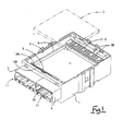
- a main body 1 of the control box is made from plastic by moulding, and an upper face thereof forms a square box shape in which a recess 2 is provided.
- Two hoods 3 and 4 are formed side by side in a unified manner on a side face of the main body 1, this side being the left anterior side face in Figure 1 .
- Rows of terminals 15A and 15B are provided as upper and lower layers within the hood 3 located on the far side, this forming a first connector member 11.
- rows of terminals 35 are provided as upper and lower layers within the hood 4, this forming a second connector member 31.
- Rows of contact members 5 and 6 are formed within the recess 2 of the upper face, the row of contact members 5 being on the side wall directly behind the connector members 11 and 31, and the row of contact members 6 being on the opposite side wall.
- a supporting frame 8 is formed between the rows of contact members 5 and 6, this supporting a printed circuit board 7.
- Contact members 18A and 18B are horizontally aligned within the row of contact members 5 located at the closer side, these contact members 18A and 18B extending from tabs 16A and 16B of the first connector member 11.
- Contact members 38 are horizontally aligned within the row of contact members 6 located at the farther side, these contact members 38 extending from tabs of the second connector member 31.
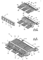
- the first connector member 11 is provided with an upper bus bar 12, a lower bus bar 13, and a position fixing plate 14.
- the upper bus bar 12 is formed by press forming an electrically conductive metal sheet, and the twelve pictured tabs 16A which comprise the upper row of terminals 15A are connected in a unified manner by a carrier 17A.
- the twelve tabs 16A are divided into three groups each comprising four tabs, the tabs 16A within each group being horizontally aligned with a prescribed distance between each tab, and with a wider distance separating the groups from one another.
- the contact members 18A extend from the posterior of each tab 16A.
- the contact members 18A after being formed sideways to the extent required, extend in a posterior direction and are consequently horizontally aligned in a manner whereby the space between each adjoining contact member 18A is greater than the space which separates the contact members 18B (to be described later) of the lower bus bar 13.
- One end of each contact member 18A is formed again at right-angles so as to protrude in a downwards and posterior direction, and is connected to the carrier 17A by a connecting member 19A.
- position fixing holes 20 are formed on both ends of the carrier 17A.
- the lower bus bar 13 is also formed by press forming an electrically conductive metal sheet, and the twelve pictured tabs 16B which comprise the lower row of terminals 15B are connected in a unified manner by a carrier 17B.
- the twelve tabs 16B are also divided into three groups each comprising four tabs, the tabs 16B within each group being horizontally aligned with a prescribed distance between each tab, and with a wider distance separating the groups from one another.
- the upper and lower bus bars 12 and 13 are placed together, the upper and lower rows of terminals 15A and 15B mutually correspond and are separated by a prescribed distance.
- the contact members 18B extend from the posterior of each tab 16B.
- these contact members 18B are horizontally aligned and fit between the contact members 18A of the upper bus bar 12.
- the contact members 18B are formed sideways from the posterior end portion of each tab 16B to the extent required, these then being raised to a height equivalent to that of the corresponding space between the upper and lower rows of terminals 15A and 15B, and then being made to extend in a posterior direction.
- the extending end of each contact member 18B is formed twice at right-angles so as to extend in a downwards and posterior direction, and is connected to the carrier 17B by a connecting member 19B.
- the carrier 17B is stepped downwards, the size of this step corresponding to the thickness of the carrier 17B.
- Position fixing holes 20 are formed on both ends of the carrier 17B, the location of these corresponding to that of the position fixing holes 20 in the carrier 17A of the upper bus bar 12.
- the carriers 17A and 17B of the upper and lower bus bars 12 and 13 are positioned one above the other with the position fixing holes 20 being together, the upper and lower rows of terminals 15A and 15B correspond with each other, separated by a prescribed distance, and the contact members 18A or 18B are aligned along a plane by mutually fitting together.
- a position fixing plate 14 is made from a plastic such as PBT resin or ABS resin, and the upper and lower rows of terminals 15A and 15B of the upper and lower bus bars 12 and 13 are inserted therethrough. Insertion holes 22 are aligned on the plate 14 to allow the upper and lower tabs 16A and 16B to be inserted. Moreover, window holes 23 pass through the plastic at prescribed locations between the insertion holes 22.
- the upper and lower bus bars 12 and 13 are positioned one above the other by aligning the carriers 17A and 17B as described above, and then the tabs 16A and 16B are inserted through the corresponding insertion holes 22 of the plate 14 as far as the base of the upper and lower rows of terminals 15A and 15B.
- the upper and lower bus bars 12 and 13 are joined together in a unified manner by the plate 14 and form an insert 25.
- This insert 25 comprises the upper and lower rows of terminals 15A and 15B corresponding to each other and separated by a prescribed distance, and the contact members 18A and 18B aligned along a plane.
- the position fixing holes 20 of the upper and lower carriers 17A and 17B match together.
- a first moulded member 27 is formed in which a housing 26 is moulded around the insert 25.
- a forming die such as that in Figure 4 .
- This forming die comprises, for example: a fixed lower mould 41; an upper mould 42 above the lower mould 41 and capable of being moved up and down; and a moveable mould 43 located to the left of the lower mould 41 and the upper mould 42 and capable of being moved to the left and right.
- a moulding cavity 44 for moulding the housing 26 is formed on the joining faces of the three moulds 41, 42 and 43.
- Fitting holes 45 are formed on the joining face of the moveable mould 43, the upper and lower tabs 16A and 16B fitting therein. Further, pins 46, pins 47, and pins 48 protrude upwards from the upper face of the lower mould 41.
- the pins 46 fit with the position fixing holes 20 of the carriers 17A and 17B, the pins 47 support the lower faces of the contact members 18A and 18B, and the pins 48 protrude upwards so as to extend along the posterior of the upwards-rising portion of the contact members 18B of the lower bus bar 13.
- the forming die is positioned in an open state as shown in Figure 4 , and the insert 25 is positioned on the upper face of the lower mould 41, with the position fixing holes 20 of the carriers 17A and 17B being fitted onto the pins 46, the lower faces of the contact members 18A and 18B making contact with the pins 47, and the posterior faces of the rising portion of the contact members 18B extending along the pins 48.
- the tabs 16A and 16B are fitted into the fitting holes 45, the moveable mould 43 is moved in a rightwards direction relative to Figure 4 , and the upper mould 42 is lowered.
- the forming die is thereby closed and the moulding cavity 44 is formed between the joining faces of the moulds 41, 42 and 43.
- molten plastic such as ABS resin etc.
- the forming die is opened after the plastic has hardened and, as shown in Figures 6 and 8 , the first moulded member 27 with the housing 26 being moulded around the insert 25 is removed.
- the housing 26 surrounds the base of the upper and lower rows of terminals 15A and 15B and supports the lower side faces of the contact members 18A and 18B which are aligned horizontally.
- the plastic has entered the window holes 23 of the plate 14, thereby unifying the housing 26 and the plate 14.
- a plurality of bosses 28 protrude from the upper face of the portion of the housing 26 surrounding the base of the rows of terminals 15A and 15B, these bosses 28 being used for binding when secondary moulding (to be explained later) is performed.
- the carriers 17A and 17B of the two bus bars 12 and 13 are cut off and removed. Specifically, this cutting off occurs on a portion slightly behind the lower edge of the descending portion of the connecting members 19A and 19B, these connecting members 19A and 19B connecting the contact members 18A and 18B to the carriers 17A and 17B.
- the portions extending behind the connecting members 19A and 19B are aligned along an identical face, and consequently the carriers 17A and 17B can be cut off by supporting this portion in the mould and press shearing a single time.
- Figures 7 and 9 show the first moulded member 27 after the carriers 17A and 17B have been cut off.
- the second connector member 31 which will be explained in less detail, is prepared by providing two rows of tabs 35 as upper and lower layers. Horizontally aligned contact members 38 protruding from the tabs are grouped together to form an insert, a housing surrounding the insert is formed within a first moulded member, and carriers are cut off in the same manner as above.
- the first moulded members of the first connector member 11 and the second connector member 31, the carriers of both having been cut off, are joined together in a unified manner in a prescribed position, this forming another insert which is secondary moulded to form the main body 1 of the control box shown in Figure 1 .
- a simplification of the production process results from using insert moulding to form a connector (first moulded member 27) whereby the terminals 15A and 15B are provided in two layers on one side of the housing 26 so as to form the insert 25 during the moulding of the main body 1 of the control box, and the other side of the housing 26 has contact members 18A and 18B aligned along a face.
- the upper and lower bus bars 12 and 13 comprising the first moulded member 27 are formed in a unified manner and joined by the carriers 17A and 17B respectively, these carriers 17A and 17B being cut off and removed after the first moulded member 27 has been moulded.
- handling is convenient during the production process, such as when the bus bars 12 and 13 are joined together, etc.
- these are joined together with the portions of the carriers 17A and 17B to be cut off being one above the other and, consequently, the carriers 17A and 17B can be cut off by shearing a single time.
- the carriers 17A and 17B are one above the other prior to being cut off, and the upper and lower bus bars 12 and 13 are in a contacting state.
- the upper and lower bus bars 12 and 13 are in a non-contacting state after the carriers 17A and 17B are cut off.
- the position fixing holes 20 are provided on both carriers 17A and 17B, these matching together when the carries 17A and 17B are joined together.
- the pins 46 in the moulding cavity 44 of the forming die fit into these position fixing holes 20, and the position of the carriers 17A and 17B within the moulding cavity 44 is thereby easily fixed.
- the plate 14 is fitted onto the base of the upper and lower rows of terminals 15A and 15B, thereby preventing the tabs 16A and 16B from shifting position whole, for example, receiving pressure from the resin during moulding. The position of the tabs 16A and 16B is thereby reliably maintained during production.
Description
- The present invention relates to an insert-moulded electrical connector and the production method thereof.
- A prior multipole appliance connector, one end of which is attached to a printed circuit board prior to use, has a plurality of terminals installed in a connector housing; these terminals are aligned in rows in order to save space, etc., and these rows are distributed in multiple layers on the side of the connector fitting with a corresponding connector. Contact members extend from each terminal on the side of the connector attached to the printed wiring board. These contact members need to be aligned in a single plane so as to be attached by wire bonding with contact points aligned on the edge of the printed circuit board.
- Conventionally, when this type of appliance connector is produced, each terminal is formed individually in a shape such that one end can be positioned in the multiple layers and the contact points of the other end can be positioned in a single plane. The housing in which attachment holes for these terminals are aligned is formed separately. Each terminal is attached by being press-fitted into a corresponding attachment hole, with the tab protruding.
- However, this conventional production method is extremely cumbersome, particularly as the multipolarity of connectors is increasing, and an improved production method is required.
- The present invention has been developed after taking the above problem into consideration and aims to present an appliance connector with a simplified production, and the production method thereof.
- According to the invention there is provided an insert-moulded electrical connector having a housing, a first row of spaced terminals each having first ends in a first plane and each having a respective contact member in a common plane, and a second row of spaced terminals interspersed within said first row and each having first ends in second plane and each having a respective contact member in said common plane, said terminals having successive right angle portions and being fixed and located as said housing is moulded about said right angled portions.
- Such a construction avoids the need for individual location of each terminal in a separately moulded housing.
- The terminals may be in two or more mutually parallel planes, but what is important is that the contact members thereof are uni-planar for connection to the edge of a printed circuit board.
- The connector may further include a position fixing member for the terminals, each terminal being located in a respective aperture of the position fixing member. This position fixing member may also be insert-moulded into the housing.
- The invention also provides a method of manufacturing an electrical connector having on one side a row of terminals in a single plane, and another side two or more rows of terminals in spaced planes, the method comprising the steps of:
- a) forming a first row of spaced terminals having connection ends in a connection plane, the terminals having a common first row carrier at said connection ends,
- b) forming a second row of spaced terminals having connection ends in a connection plane, the terminals having a common second row carrier at said connection ends,
- c) placing said carriers one above the other such that said first and second row of terminals are interspersed adjacent said carriers,
- d) forming a plastics housing to fix and locate said terminals by insert moulding about right angled portions of said terminals, and
- e) shearing said carriers from said first and second rows of terminals, thereby rendering each of said terminals electrically independent whilst being fixed in said housing.
- The method may include the preliminary step of forming mutually alignable apertures in the common carriers, and aligning those apertures in the mould with mould alignment pins. Such an arrangement ensures precise location and positioning prior to insert moulding.
- Other features of the invention are disclosed in the following description of a preferred embodiment shown by way of example only in the accompanying drawings, in which:
-
Figure 1 is a diagonal view of a control box of an embodiment of the present invention. -
Figure 2 is a disassembled diagonal view of an insert for connector housing. -
Figure 3 is a diagonal view of the assembled insert. -
Figure 4 is a cross-sectional view of a forming die of the connector housing, the die being in an open state. -
Figure 5 is a cross-sectional view of the die in a closed state. -
Figure 6 is a cross-sectional view of the moulded housing. -
Figure 7 is a cross-sectional view of the moulded housing after carriers have been cut off. -
Figure 8 is a diagonal view of the moulded housing. -
Figure 9 is a diagonal view of the moulded housing after the carriers have been cut off. - An embodiment of the present invention is explained below with the aid of
Figures 1 to 9 . This embodiment illustrates a connector suitable for use in a control box of an automobile. - First, the overall configuration of the control box will be explained with reference to
Figure 1 . Amain body 1 of the control box is made from plastic by moulding, and an upper face thereof forms a square box shape in which arecess 2 is provided. Twohoods 3 and 4 are formed side by side in a unified manner on a side face of themain body 1, this side being the left anterior side face inFigure 1 . Rows ofterminals first connector member 11. In the same manner, rows ofterminals 35 are provided as upper and lower layers within thehood 4, this forming asecond connector member 31. Rows ofcontact members recess 2 of the upper face, the row ofcontact members 5 being on the side wall directly behind theconnector members contact members 6 being on the opposite side wall. A supportingframe 8 is formed between the rows ofcontact members circuit board 7. - Contact
members contact members 5 located at the closer side, thesecontact members tabs first connector member 11. Contactmembers 38 are horizontally aligned within the row ofcontact members 6 located at the farther side, thesecontact members 38 extending from tabs of thesecond connector member 31. After theboard 7 has been fitted into the supportingframe 8, contact points provided on the sides of theboard 7 make contact with thecorresponding contact members contact members 38, and are fixed by wire bonding. - Next, the production sequence is explained, with the focus on the
first connector member 11. - As
Figure 2 shows, thefirst connector member 11 is provided with anupper bus bar 12, alower bus bar 13, and aposition fixing plate 14. - The
upper bus bar 12 is formed by press forming an electrically conductive metal sheet, and the twelve picturedtabs 16A which comprise the upper row ofterminals 15A are connected in a unified manner by acarrier 17A. The twelvetabs 16A are divided into three groups each comprising four tabs, thetabs 16A within each group being horizontally aligned with a prescribed distance between each tab, and with a wider distance separating the groups from one another. - The
contact members 18A extend from the posterior of eachtab 16A. Thecontact members 18A, after being formed sideways to the extent required, extend in a posterior direction and are consequently horizontally aligned in a manner whereby the space between each adjoiningcontact member 18A is greater than the space which separates thecontact members 18B (to be described later) of thelower bus bar 13. One end of eachcontact member 18A is formed again at right-angles so as to protrude in a downwards and posterior direction, and is connected to thecarrier 17A by a connectingmember 19A.position fixing holes 20 are formed on both ends of thecarrier 17A. - The
lower bus bar 13 is also formed by press forming an electrically conductive metal sheet, and the twelve picturedtabs 16B which comprise the lower row ofterminals 15B are connected in a unified manner by acarrier 17B. The twelvetabs 16B are also divided into three groups each comprising four tabs, thetabs 16B within each group being horizontally aligned with a prescribed distance between each tab, and with a wider distance separating the groups from one another. As will be explained below, when the upper andlower bus bars terminals - The
contact members 18B extend from the posterior of eachtab 16B. When the upper and lower rows ofterminals contact members 18B are horizontally aligned and fit between thecontact members 18A of theupper bus bar 12. For this purpose, thecontact members 18B are formed sideways from the posterior end portion of eachtab 16B to the extent required, these then being raised to a height equivalent to that of the corresponding space between the upper and lower rows ofterminals contact member 18B is formed twice at right-angles so as to extend in a downwards and posterior direction, and is connected to thecarrier 17B by a connectingmember 19B. As shown inFigure 4 , thecarrier 17B is stepped downwards, the size of this step corresponding to the thickness of thecarrier 17B. Position fixing holes 20 are formed on both ends of thecarrier 17B, the location of these corresponding to that of theposition fixing holes 20 in thecarrier 17A of theupper bus bar 12. - The
carriers position fixing holes 20 being together, the upper and lower rows ofterminals contact members - A
position fixing plate 14 is made from a plastic such as PBT resin or ABS resin, and the upper and lower rows ofterminals plate 14 to allow the upper andlower tabs - The upper and lower bus bars 12 and 13 are positioned one above the other by aligning the
carriers tabs plate 14 as far as the base of the upper and lower rows ofterminals Figure 3 , the upper and lower bus bars 12 and 13 are joined together in a unified manner by theplate 14 and form aninsert 25. Thisinsert 25 comprises the upper and lower rows ofterminals contact members position fixing holes 20 of the upper andlower carriers - Next, a first moulded
member 27 is formed in which ahousing 26 is moulded around theinsert 25. - For this purpose, a forming die is provided such as that in
Figure 4 . This forming die comprises, for example: a fixedlower mould 41; anupper mould 42 above thelower mould 41 and capable of being moved up and down; and amoveable mould 43 located to the left of thelower mould 41 and theupper mould 42 and capable of being moved to the left and right. Amoulding cavity 44 for moulding thehousing 26 is formed on the joining faces of the threemoulds holes 45 are formed on the joining face of themoveable mould 43, the upper andlower tabs lower mould 41. Thepins 46 fit with theposition fixing holes 20 of thecarriers pins 47 support the lower faces of thecontact members pins 48 protrude upwards so as to extend along the posterior of the upwards-rising portion of thecontact members 18B of thelower bus bar 13. - In order to mould the first moulded
member 27, the forming die is positioned in an open state as shown inFigure 4 , and theinsert 25 is positioned on the upper face of thelower mould 41, with theposition fixing holes 20 of thecarriers pins 46, the lower faces of thecontact members pins 47, and the posterior faces of the rising portion of thecontact members 18B extending along thepins 48. Next, thetabs moveable mould 43 is moved in a rightwards direction relative toFigure 4 , and theupper mould 42 is lowered. The forming die is thereby closed and themoulding cavity 44 is formed between the joining faces of themoulds - From this state, molten plastic such as ABS resin etc., is injected into the
moulding cavity 44 through a gate (not shown), the forming die is opened after the plastic has hardened and, as shown inFigures 6 and8 , the first mouldedmember 27 with thehousing 26 being moulded around theinsert 25 is removed. Thehousing 26 surrounds the base of the upper and lower rows ofterminals contact members plate 14, thereby unifying thehousing 26 and theplate 14. Moreover, a plurality ofbosses 28 protrude from the upper face of the portion of thehousing 26 surrounding the base of the rows ofterminals bosses 28 being used for binding when secondary moulding (to be explained later) is performed. - After the first moulded
member 27 has been formed in the manner described above, thecarriers bus bars members members contact members carriers members carriers Figures 7 and9 show the first mouldedmember 27 after thecarriers - The
second connector member 31, which will be explained in less detail, is prepared by providing two rows oftabs 35 as upper and lower layers. Horizontally alignedcontact members 38 protruding from the tabs are grouped together to form an insert, a housing surrounding the insert is formed within a first moulded member, and carriers are cut off in the same manner as above. - The first moulded members of the
first connector member 11 and thesecond connector member 31, the carriers of both having been cut off, are joined together in a unified manner in a prescribed position, this forming another insert which is secondary moulded to form themain body 1 of the control box shown inFigure 1 . - According to the embodiment explained above, a simplification of the production process results from using insert moulding to form a connector (first moulded member 27) whereby the
terminals housing 26 so as to form theinsert 25 during the moulding of themain body 1 of the control box, and the other side of thehousing 26 hascontact members - The upper and lower bus bars 12 and 13 comprising the first moulded
member 27 are formed in a unified manner and joined by thecarriers carriers member 27 has been moulded. As a result, handling is convenient during the production process, such as when the bus bars 12 and 13 are joined together, etc. Further, these are joined together with the portions of thecarriers carriers carriers carriers - The position fixing holes 20 are provided on both
carriers pins 46 in themoulding cavity 44 of the forming die fit into theseposition fixing holes 20, and the position of thecarriers moulding cavity 44 is thereby easily fixed. - Furthermore, after the bus bars 12 and 13 are joined together, the
plate 14 is fitted onto the base of the upper and lower rows ofterminals tabs tabs - The present invention is not limited to the embodiments described above with the aid of figures. For example, the possibilities described below also lie within the technical range of the present invention. In addition, the present invention may be embodied in various other ways without deviating from the scope thereof.
- (1) The rows of tabs may also be provided as three or more layers.
- (2) In the preferred embodiment, the connecting members are short; they could however be much larger depending on the configuration of the connector assembly.
Claims (8)
- An insert-moulded electrical connector having a housing (26), a first row of spaced terminals (15A) each having first ends in a first plane and each having a respective contact member (18A) in a common plane, and a second row of spaced terminals (15B) interspersed within said first row and each having first ends in second plane and each having a respective contact member (18B) in said common plane, said terminals having successive right angle portions and being fixed and located as said housing (26) is moulded about said right angled portions.
- A connector according to claim 1 wherein said first and second rows of terminals (15A,15B) are in mutually parallel planes.
- A connector according to any preceding claim and further including a position fixing member (14) for said terminals (15A,15B), said position fixing member (14) having a plurality of apertures (22) in said first and second planes, and each of said terminals passing through a respective one of said apertures.
- A connector according to any preceding claim wherein said first and second rows of terminals are respectively connected by common carriers (17A, 17B).
- A connector according to claim 4 wherein said contact members (18A,18B) are connected to said common carriers (17A,17B) by respective connecting members (19A, 19B), the connecting members lying in a common plane.
- A method of manufacturing an electrical connector having on one side a row of terminals in a single plane, and on another side two or more rows of terminals in spaced planes, the method comprising the steps ofa) forming a first row of spaced terminals having connection ends in a connection plane, the terminals having a common first row carrier at said connection ends,b) forming a second row of spaced terminals having connection ends in a connection plane, the terminals having a common second row carrier at said connection ends,c) placing said carriers one above the other such that said first and second row of terminals are interspersed adjacent said carriers,d) forming a plastics housing to fix and locate said terminals by insert moulding about right angled portions of said terminals, ande) shearing said carriers from said first and second rows of terminals, thereby rendering each of said terminals electrically independent whilst being fixed in said housing.
- A method according to claim 6 and including the additional steps ofc2) placing a position fixing member over said terminals, said position fixing member having a respective aperture for each of said terminals, andd2) insert-moulding said position fixing member as said plastics housing is formed.
- A method according to claim 6 or claim 7 and including the steps ofa2, b2) providing aligned apertures in said common carriers; andd3) providing alignment pins in a plastics mould for location in said apertures during insert-moulding, thereby to prevent relative movement of said terminals during insert moulding.
Applications Claiming Priority (2)
| Application Number | Priority Date | Filing Date | Title |
|---|---|---|---|
| JP16988398 | 1998-06-17 | ||
| JP16988398A JP3405201B2 (en) | 1998-06-17 | 1998-06-17 | Manufacturing method of equipment connector |
Publications (2)
| Publication Number | Publication Date |
|---|---|
| EP0966075A1 EP0966075A1 (en) | 1999-12-22 |
| EP0966075B1 true EP0966075B1 (en) | 2008-05-14 |
Family
ID=15894731
Family Applications (1)
| Application Number | Title | Priority Date | Filing Date |
|---|---|---|---|
| EP99304646A Expired - Lifetime EP0966075B1 (en) | 1998-06-17 | 1999-06-15 | Appliance connector and production method thereof |
Country Status (5)
| Country | Link |
|---|---|
| US (1) | US6217393B1 (en) |
| EP (1) | EP0966075B1 (en) |
| JP (1) | JP3405201B2 (en) |
| CN (1) | CN1134863C (en) |
| DE (1) | DE69938694D1 (en) |
Families Citing this family (17)
| Publication number | Priority date | Publication date | Assignee | Title |
|---|---|---|---|---|
| SG80641A1 (en) * | 1999-08-30 | 2001-05-22 | Fci Singapore Ltd | Method for manufacturing electrical connectors for enhancing coplanarity |
| DE10045073B4 (en) * | 2000-09-12 | 2005-03-03 | Siemens Ag | Plug element and associated manufacturing method |
| DE10120362A1 (en) * | 2001-04-26 | 2002-11-21 | Integrated Electronic Systems Sys Consulting Gmbh | Injection molding |
| JP2002343475A (en) * | 2001-05-21 | 2002-11-29 | Nagano Fujitsu Component Kk | Stm connector and manufacturing method therefor |
| US6832936B2 (en) * | 2002-10-17 | 2004-12-21 | Molex Incorporated | Terminal module for electrical connector |
| US6692273B1 (en) * | 2002-12-31 | 2004-02-17 | Hon Hai Precision Ind. Co., Ltd. | Straddle mount connector |
| KR100796731B1 (en) | 2006-08-02 | 2008-01-21 | 이승희 | A electric contact blank and the method for packing thereof |
| US7371118B2 (en) * | 2006-08-25 | 2008-05-13 | Hon Hai Precision Ind. Co., Ltd | Electrical connector assembly with reduced crosstalk and electromaganetic interference |
| DE102006062313A1 (en) * | 2006-12-27 | 2008-07-03 | Robert Bosch Gmbh | Electrical plug connector, has parallel connector pins and connection contacts, which are connected with each other by rigid conductive strips, and lateral bucklings of conductive strips formed as arc shaped or meander-shaped |
| JP5632217B2 (en) | 2010-07-08 | 2014-11-26 | 矢崎総業株式会社 | Connector insert molding method |
| JP6057069B2 (en) * | 2013-01-30 | 2017-01-11 | 第一精工株式会社 | Collective type electrical connector and collective type electrical connector manufacturing method |
| CN104733977A (en) * | 2013-12-18 | 2015-06-24 | 江苏景联电子科技有限公司 | Connector manufacturing method |
| US20160344118A1 (en) * | 2015-05-19 | 2016-11-24 | Ching-Ho (NMI) Hsieh | Separable Electrical Connector and Method of Making It |
| CN105655839A (en) * | 2016-01-26 | 2016-06-08 | 沈阳兴华航空电器有限责任公司 | Inlaying plastic compressing sealing method for contact element |
| JP6390663B2 (en) * | 2016-05-18 | 2018-09-19 | 第一精工株式会社 | Electrical connector and manufacturing method thereof |
| USD840030S1 (en) | 2016-06-02 | 2019-02-05 | Intarcia Therapeutics, Inc. | Implant placement guide |
| JP2019176675A (en) * | 2018-03-29 | 2019-10-10 | 日本電産株式会社 | motor |
Family Cites Families (5)
| Publication number | Priority date | Publication date | Assignee | Title |
|---|---|---|---|---|
| US3391456A (en) * | 1965-04-30 | 1968-07-09 | Sylvania Electric Prod | Multiple segment array making |
| US4602830A (en) * | 1984-09-20 | 1986-07-29 | Amp Incorporated | Double row electrical connector |
| US4639056A (en) * | 1985-05-31 | 1987-01-27 | Trw Inc. | Connector construction for a PC board or the like |
| US5201662A (en) | 1991-08-23 | 1993-04-13 | Molex Incorporated | Electrical connector for mounting on a printed circuit board |
| US5267875A (en) * | 1993-04-27 | 1993-12-07 | The Whitaker Corporation | Electrical connector assembly |
-
1998
- 1998-06-17 JP JP16988398A patent/JP3405201B2/en not_active Expired - Fee Related
-
1999
- 1999-06-11 CN CNB991090179A patent/CN1134863C/en not_active Expired - Fee Related
- 1999-06-15 EP EP99304646A patent/EP0966075B1/en not_active Expired - Lifetime
- 1999-06-15 DE DE69938694T patent/DE69938694D1/en not_active Expired - Lifetime
- 1999-06-16 US US09/333,975 patent/US6217393B1/en not_active Expired - Lifetime
Also Published As
| Publication number | Publication date |
|---|---|
| DE69938694D1 (en) | 2008-06-26 |
| EP0966075A1 (en) | 1999-12-22 |
| US6217393B1 (en) | 2001-04-17 |
| JP3405201B2 (en) | 2003-05-12 |
| CN1134863C (en) | 2004-01-14 |
| JP2000012170A (en) | 2000-01-14 |
| CN1239338A (en) | 1999-12-22 |
Similar Documents
| Publication | Publication Date | Title |
|---|---|---|
| EP0966075B1 (en) | Appliance connector and production method thereof | |
| EP1356550B1 (en) | Connector moulding method and shielded waferized connector made therefrom | |
| US6065951A (en) | Mold for use in manufacturing an electrical connector | |
| US6007387A (en) | Connector producing method and a connector produced by insert molding | |
| JP3414402B2 (en) | Electrical connectors, housings and contacts | |
| EP1014501A1 (en) | An electrical connection box, its method of manufacturing, a wire connection busbar of an electrical connection box and its producing method | |
| US5611699A (en) | Tape-carrier-type electrical connector and method of manufacturing same | |
| US6368158B1 (en) | Electric connector having integrally molded terminals and guide pins | |
| US6517386B2 (en) | Electrical connector and method of making the same | |
| US6000971A (en) | Multi-stage connector and method for producing and assembling the same | |
| JPH10255950A (en) | Manufacture of electric connector | |
| JPH11345675A (en) | Manufacture of electric connector | |
| EP0702434B1 (en) | Molded electrical connector | |
| US20010031584A1 (en) | Hybrid plug housing and process for its production | |
| JPH07282912A (en) | Terminal array and manufacture thereof | |
| JPH0879943A (en) | Wiring method for wiring board assembly | |
| WO1998000885A1 (en) | Electrical connector | |
| JP2003070131A (en) | Junction box and method for molding case of the same | |
| JPH03122988A (en) | Method of forming electric terminal | |
| JPH033448B2 (en) |
Legal Events
| Date | Code | Title | Description |
|---|---|---|---|
| PUAI | Public reference made under article 153(3) epc to a published international application that has entered the european phase |
Free format text: ORIGINAL CODE: 0009012 |
|
| 17P | Request for examination filed |
Effective date: 19990706 |
|
| AK | Designated contracting states |
Kind code of ref document: A1 Designated state(s): DE FR GB IT |
|
| AX | Request for extension of the european patent |
Free format text: AL;LT;LV;MK;RO;SI |
|
| AKX | Designation fees paid |
Free format text: DE FR GB IT |
|
| GRAP | Despatch of communication of intention to grant a patent |
Free format text: ORIGINAL CODE: EPIDOSNIGR1 |
|
| GRAS | Grant fee paid |
Free format text: ORIGINAL CODE: EPIDOSNIGR3 |
|
| GRAA | (expected) grant |
Free format text: ORIGINAL CODE: 0009210 |
|
| AK | Designated contracting states |
Kind code of ref document: B1 Designated state(s): DE FR GB IT |
|
| REG | Reference to a national code |
Ref country code: GB Ref legal event code: FG4D |
|
| REF | Corresponds to: |
Ref document number: 69938694 Country of ref document: DE Date of ref document: 20080626 Kind code of ref document: P |
|
| PGFP | Annual fee paid to national office [announced via postgrant information from national office to epo] |
Ref country code: IT Payment date: 20080625 Year of fee payment: 10 |
|
| PGFP | Annual fee paid to national office [announced via postgrant information from national office to epo] |
Ref country code: GB Payment date: 20080618 Year of fee payment: 10 |
|
| PLBE | No opposition filed within time limit |
Free format text: ORIGINAL CODE: 0009261 |
|
| STAA | Information on the status of an ep patent application or granted ep patent |
Free format text: STATUS: NO OPPOSITION FILED WITHIN TIME LIMIT |
|
| 26N | No opposition filed |
Effective date: 20090217 |
|
| GBPC | Gb: european patent ceased through non-payment of renewal fee |
Effective date: 20090615 |
|
| PG25 | Lapsed in a contracting state [announced via postgrant information from national office to epo] |
Ref country code: GB Free format text: LAPSE BECAUSE OF NON-PAYMENT OF DUE FEES Effective date: 20090615 |
|
| PGFP | Annual fee paid to national office [announced via postgrant information from national office to epo] |
Ref country code: FR Payment date: 20100709 Year of fee payment: 12 |
|
| PGFP | Annual fee paid to national office [announced via postgrant information from national office to epo] |
Ref country code: DE Payment date: 20100610 Year of fee payment: 12 |
|
| PG25 | Lapsed in a contracting state [announced via postgrant information from national office to epo] |
Ref country code: IT Free format text: LAPSE BECAUSE OF NON-PAYMENT OF DUE FEES Effective date: 20090615 |
|
| REG | Reference to a national code |
Ref country code: FR Ref legal event code: ST Effective date: 20120229 |
|
| REG | Reference to a national code |
Ref country code: DE Ref legal event code: R119 Ref document number: 69938694 Country of ref document: DE Effective date: 20120103 |
|
| PG25 | Lapsed in a contracting state [announced via postgrant information from national office to epo] |
Ref country code: FR Free format text: LAPSE BECAUSE OF NON-PAYMENT OF DUE FEES Effective date: 20110630 Ref country code: DE Free format text: LAPSE BECAUSE OF NON-PAYMENT OF DUE FEES Effective date: 20120103 |