EP0965819A1 - Schnittstellenschaltungsanordnung für piezoelektrischen Sensor - Google Patents
Schnittstellenschaltungsanordnung für piezoelektrischen Sensor Download PDFInfo
- Publication number
- EP0965819A1 EP0965819A1 EP98810546A EP98810546A EP0965819A1 EP 0965819 A1 EP0965819 A1 EP 0965819A1 EP 98810546 A EP98810546 A EP 98810546A EP 98810546 A EP98810546 A EP 98810546A EP 0965819 A1 EP0965819 A1 EP 0965819A1
- Authority
- EP
- European Patent Office
- Prior art keywords
- sensor
- current
- signal
- electronic circuit
- cable
- Prior art date
- Legal status (The legal status is an assumption and is not a legal conclusion. Google has not performed a legal analysis and makes no representation as to the accuracy of the status listed.)
- Granted
Links
- 238000005259 measurement Methods 0.000 claims description 29
- 230000007257 malfunction Effects 0.000 claims description 3
- 230000008030 elimination Effects 0.000 claims description 2
- 238000003379 elimination reaction Methods 0.000 claims description 2
- 239000003990 capacitor Substances 0.000 claims 1
- 230000003071 parasitic effect Effects 0.000 abstract description 3
- 238000010586 diagram Methods 0.000 description 18
- 230000005540 biological transmission Effects 0.000 description 2
- 230000003321 amplification Effects 0.000 description 1
- 101150083534 cpar-1 gene Proteins 0.000 description 1
- 235000021183 entrée Nutrition 0.000 description 1
- 238000009413 insulation Methods 0.000 description 1
- 239000012212 insulator Substances 0.000 description 1
- 238000000034 method Methods 0.000 description 1
- 238000012544 monitoring process Methods 0.000 description 1
- 238000003199 nucleic acid amplification method Methods 0.000 description 1
- 244000045947 parasite Species 0.000 description 1
- 230000000284 resting effect Effects 0.000 description 1
Images

Classifications
-
- G—PHYSICS
- G01—MEASURING; TESTING
- G01D—MEASURING NOT SPECIALLY ADAPTED FOR A SPECIFIC VARIABLE; ARRANGEMENTS FOR MEASURING TWO OR MORE VARIABLES NOT COVERED IN A SINGLE OTHER SUBCLASS; TARIFF METERING APPARATUS; MEASURING OR TESTING NOT OTHERWISE PROVIDED FOR
- G01D3/00—Indicating or recording apparatus with provision for the special purposes referred to in the subgroups
- G01D3/028—Indicating or recording apparatus with provision for the special purposes referred to in the subgroups mitigating undesired influences, e.g. temperature, pressure
- G01D3/036—Indicating or recording apparatus with provision for the special purposes referred to in the subgroups mitigating undesired influences, e.g. temperature, pressure on measuring arrangements themselves
-
- G—PHYSICS
- G01—MEASURING; TESTING
- G01L—MEASURING FORCE, STRESS, TORQUE, WORK, MECHANICAL POWER, MECHANICAL EFFICIENCY, OR FLUID PRESSURE
- G01L1/00—Measuring force or stress, in general
- G01L1/16—Measuring force or stress, in general using properties of piezoelectric devices
-
- G—PHYSICS
- G01—MEASURING; TESTING
- G01N—INVESTIGATING OR ANALYSING MATERIALS BY DETERMINING THEIR CHEMICAL OR PHYSICAL PROPERTIES
- G01N2291/00—Indexing codes associated with group G01N29/00
- G01N2291/02—Indexing codes associated with the analysed material
- G01N2291/028—Material parameters
- G01N2291/02827—Elastic parameters, strength or force
Definitions
- the invention relates to an electronic interface circuit according to the preamble of claim 1.
- Piezoelectric sensors are used for example to measure the vibrations of a machine.
- the sensor housing is attached to the machine and signals obtained with the sensor and representative of machine vibrations are transmitted through a cable to a electronic circuit for processing the measurement signal obtained with the sensor.
- This last circuit can be very away from the sensor.
- potential common mode parasites also called "frame voltage” and which is often referred to as Uframe appear between the sensor housing and the earth (level voltage 0 V) of the electronic circuit for processing of the measurement signal and generate an error voltage superimposed on the measurement signal obtained with the sensor.
- this object is achieved with a circuit electronic interface (IEC) with the elements defined in the characterizing part of the claim 1.
- IEC circuit electronic interface
- Such an electronic interface circuit (IEC) allows advantageously to form a measurement chain allowing achieve the goals 1) to 3) mentioned above, and allows especially not to need a transformer bulky and relatively expensive to obtain a decoupling between the electronic circuit connected to the sensor and the electronic circuit for signal processing measured.
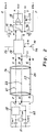
- Figure 1 shows the block diagram of a circuit electronic interface according to the invention and having the function of an interface between a measurement circuit comprising a piezoelectric sensor and a circuit 12 for the processing of the measurement signal obtained with the sensor.
- IEC the circuit electronic interface according to the invention
- circuit 12 is simply called read circuit 12, although its function is not necessarily limited on reading the said measurement signal.
- a measurement circuit comprising a sensor piezoelectric 11 and an integrated electronic circuit 13 with it is housed in a case 25.
- Such a circuit measurement is symbolically represented in Figure 1 by the series connection of a DC voltage source 27 providing a DC voltage Udc and a source of alternating voltage 28 providing a voltage Uac.
- a voltage source 29 represents a parasitic voltage Ucm, common mode voltage produced by Uframe voltage mentioned above.
- the measuring circuit which we have just described is connected to the rest of the system shown in Figure 1 by means of a cable symbolically represented by a block 14.
- an IEC according to the invention serves, on the one hand, to supply the said piezoelectric sensor with a constant current, and on the other hand, to condition an electrical signal obtained from this sensor through an electronic circuit, which includes, for example, a voltage modulator (voltage modulator) having a high input impedance.
- the CEI according to the invention is connected to the piezoelectric sensor by a cable not shown in Figure 1, but shown in details in Figures 2 to 4.
- the IEC according to the invention and the reading circuit 12 are housed in a housing 26 shown in Figure 1 by a dotted line.
- the box 26 is the mass M of the CEI, i.e. it is found at a voltage level, which represents the level of voltage 0 V for the IEC according to the invention and for the read circuit 12 connected thereto.
- the first current source 15 is intended to provide a first constant current I1 to said sensor 11 through a electric current loop.
- a terminal S from the source of current 15 is connected to the positive terminal of a source of direct voltage 38, which provides a voltage UAL +.
- the second current source 16 is intended to absorb a second constant current I2, which returns from said sensor 11 to said electronic circuit through said loop when said sensor 11 is supplied with said first current I1.
- a terminal T of the current source 16 is connected to the negative terminal of a voltage source continuous 39, which provides a voltage UAL-.
- the current loop includes the current source 15, the terminal P, the circuit connected to terminals P, Q comprising the piezoelectric sensor, the Q terminal, and the source of stream 16.
- Impedance Zo consists of an electrical resistance Ro connected in parallel with a capacitor Co. The difference between the two currents is absorbed by Zo.
- the circuit is configured and dimensioned so that I1 is very close to I2, so that the voltage developing on Ro be as low as possible. In practical there is always a small difference between I1 and I2, which is due to the tolerances of the components used.
- the high-pass filter 17 is used to decouple and thereby eliminate the DC component of the electrical signal obtained by means of said piezoelectric sensor 11 and to be supplied to the read circuit 12 a signal without said component.
- the said continuous component of the electrical signal obtained is the quiescent voltage, Udc, of the current loop.
- Voltage Udc is represented in the schematic diagram of Figure 1 as a voltage developing across the terminals of the voltage source 27, which forms from the diagram equivalent of the sensor 11 shown there.
- the differential amplifier stage 18 has a high impedance input used to reject the common mode potential (frame voltage) and amplification of the AC signal Uac supplied by the piezoelectric sensor.
- the amplifier differential 18 is preferably an amplifier instrumentation.
- the entrance to floor 18 is connected with the output of the high-pass filter 17.
- the output (terminals X, Y) of stage 18 provides a signal Uout at the input of read circuit 12.
- an IEC further comprises a filter 19 for elimination electromagnetic disturbances, said filter 19 being inserted between terminals C, D of the second end of the cable and the input terminals P, Q of said high-pass filter.
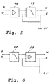
- Figure 5 shows a block diagram of an additional part added to the circuit represented by the block diagram of Fig. 1.
- This additional part includes a differential amplifier 48 having a high impedance input whose input is connected to terminals P and Q of the diagram represents in figure 1.
- the amplifier differential 48 is followed by a low-pass filter 47 used to reject the signal component representing the quantity physics measured with the piezoelectric sensor 11 and keep and deliver to terminals W, Z only one signal corresponding to the DC component of the signal, i.e. a signal corresponding to the resting voltage of the loop.
- Figure 6 shows a block diagram of part which can be added to the diagram principle of FIG. 1 instead of the additional part represented by figure 5 in order to obtain a function additional with an electronic interface circuit according to the invention.
- the additional part shown in Figure 6 includes a low-pass filter 57 and an amplifier stage 58.
- the low pass filter 57 has a high input impedance and receives at its input an electrical signal obtained from sensor 11 at through the cable 14, 34.
- the low-pass filter 57 serves to eliminate the component of the signal obtained with the sensor, which corresponds to the physical quantity measured with this one, and to provide as an output signal a signal representative of the DC component of said signal.
- the input of the amplifier stage 58 is connected with the output of said low-pass filter 57.
- the output signal of the amplifier stage 58 makes it possible to detect a malfunction in connection between sensor and the interface electronic circuit.
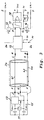
- FIG. 2 shows a measurement chain, in which a CEI according to the invention is used on the one hand to supply a sensor piezoelectric 11 with constant current and secondly to condition an electrical signal obtained from this sensor 11 through an electronic circuit 13 integrated with this sensor.
- This electronic circuit 13 essentially comprises a voltage modulator 13, which is supplied with current. Instead of a voltage modulator you can use a load / voltage converter supplied with current. In one preferred embodiment the voltage modulator or the charge / voltage converter used in its place are followed an integrating stage.
- the piezoelectric sensor 11 and the electronic circuit 13 integrated with it are isolated from the housing 25, in which the sensor 11 and its integrated electronic circuit 13 are housed.
- Ccap capacity mentioned in figure 2 next to the sensor 11 represents the electrical capacity of the sensor measuring element himself.
- Cpar1 and Cpar2 represent the capacities interference between the sensor and the housing 25.
- a cable 14 with 2 strands 21, 22 and having shielding 23 covered an insulator 24 is used for the interconnection of the IEC according to the invention (represented in the right dimension of the diagram in Figure 2) with the piezoelectric sensor 11 and the electronic circuit 13 integrated therewith.
- terminals F, G of one end of the cable 14 are connected to the terminals J, K at the output of the electronic circuit 13 and the two corresponding terminals C, D on the opposite end of the cable 14 are connected to terminals A, B of the IEC according to the invention.
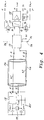
- Figure 3 shows a measurement chain with a structure similar to that shown in Figure 2, but in which a cable 34 to 1 strand 41 and with a shield 43 covered with insulation 44 is used for interconnection of the IEC according to the invention (shown on the right side of the diagram in Figure 3) with the piezoelectric sensor 11 and the electronic circuit 13 integrated with it.
- Cable 34 is preferably an insulated coaxial cable.
- Figure 4 shows a measurement chain with a structure almost identical to that shown in Figure 3, but in which the terminal K of the electronic circuit 13 integrated with the sensor 11 is connected with the housing 25.
- the measurement chain shown in Figure 4 we obtains the same operating characteristics as with the measurement chain shown in Figure 3.
Landscapes
- Physics & Mathematics (AREA)
- General Physics & Mathematics (AREA)
- Arrangements For Transmission Of Measured Signals (AREA)
- Gyroscopes (AREA)
Priority Applications (6)
| Application Number | Priority Date | Filing Date | Title |
|---|---|---|---|
| EP98810546A EP0965819B1 (de) | 1998-06-16 | 1998-06-16 | Schnittstellenschaltungsanordnung für piezoelektrischen Sensor |
| ES98810546T ES2226088T3 (es) | 1998-06-16 | 1998-06-16 | Circuito electronico de interface para un sensor piezoelectrico. |
| DK98810546T DK0965819T3 (da) | 1998-06-16 | 1998-06-16 | Elektronisk interfacekredslöb til en piezoelektrisk sensor |
| DE1998625429 DE69825429T2 (de) | 1998-06-16 | 1998-06-16 | Schnittstellenschaltungsanordnung für piezoelektrischen Sensor |
| US09/311,535 US6107881A (en) | 1998-06-16 | 1999-05-13 | Electronic interface circuit between a piezoelectric transducer and a circuit for processing a measuring signal provided by the transducer |
| CA002272166A CA2272166C (en) | 1998-06-16 | 1999-05-18 | An electronic interface circuit between a piezoelectric transducer and a circuit for processing a measuring signal provided by the transducer |
Applications Claiming Priority (1)
| Application Number | Priority Date | Filing Date | Title |
|---|---|---|---|
| EP98810546A EP0965819B1 (de) | 1998-06-16 | 1998-06-16 | Schnittstellenschaltungsanordnung für piezoelektrischen Sensor |
Publications (2)
| Publication Number | Publication Date |
|---|---|
| EP0965819A1 true EP0965819A1 (de) | 1999-12-22 |
| EP0965819B1 EP0965819B1 (de) | 2004-08-04 |
Family
ID=8236136
Family Applications (1)
| Application Number | Title | Priority Date | Filing Date |
|---|---|---|---|
| EP98810546A Expired - Lifetime EP0965819B1 (de) | 1998-06-16 | 1998-06-16 | Schnittstellenschaltungsanordnung für piezoelektrischen Sensor |
Country Status (6)
| Country | Link |
|---|---|
| US (1) | US6107881A (de) |
| EP (1) | EP0965819B1 (de) |
| CA (1) | CA2272166C (de) |
| DE (1) | DE69825429T2 (de) |
| DK (1) | DK0965819T3 (de) |
| ES (1) | ES2226088T3 (de) |
Cited By (1)
| Publication number | Priority date | Publication date | Assignee | Title |
|---|---|---|---|---|
| WO2012095546A1 (es) * | 2011-01-14 | 2012-07-19 | Eads Construcciones Aeronauticas, S.A. | Dispositivo para dotar de alta inmunidad al ruido a señales eléctricas |
Families Citing this family (3)
| Publication number | Priority date | Publication date | Assignee | Title |
|---|---|---|---|---|
| RU2327172C2 (ru) * | 2006-08-09 | 2008-06-20 | Общество с ограниченной ответственностью "ДИАМЕХ-2000" | Согласующее устройство для пьезоакселерометра |
| JP7608715B2 (ja) * | 2020-01-28 | 2025-01-07 | 株式会社リコー | インソール、及び履物 |
| US20230028286A1 (en) * | 2020-01-24 | 2023-01-26 | Ricoh Company, Ltd. | Sensor element and sensor system |
Citations (3)
| Publication number | Priority date | Publication date | Assignee | Title |
|---|---|---|---|---|
| US5220836A (en) * | 1989-04-27 | 1993-06-22 | AVL Gesellschaft fur Verbrennungskraftmaschinen und Messtechnick mbH., Prof.Dr.Dr.h.c. Hans List | Method and arrangement for piezoelectric measurement |
| US5339285A (en) * | 1993-04-12 | 1994-08-16 | The United States Of America As Represented By The Secretary Of The Navy | Monolithic low noise preamplifier for piezoelectric sensors |
| US5371469A (en) * | 1993-02-16 | 1994-12-06 | The United States Of America As Represented By The Administrator Of The National Aeronautics And Space Administration | Constant current loop impedance measuring system that is immune to the effects of parasitic impedances |
Family Cites Families (4)
| Publication number | Priority date | Publication date | Assignee | Title |
|---|---|---|---|---|
| US3982425A (en) * | 1974-01-14 | 1976-09-28 | Rockwell International Corporation | Ultrasonic inspection system |
| US4393347A (en) * | 1980-08-06 | 1983-07-12 | Action Instruments Co. Inc. | Common mode voltage rejection circuit |
| US4979218A (en) * | 1989-05-01 | 1990-12-18 | Audio Teknology Incorporated | Balanced output circuit |
| US5856891A (en) * | 1997-01-22 | 1999-01-05 | Vtc Inc. | MR resistive-biasing scheme providing low noise high common-mode rejection and high supply rejection |
-
1998
- 1998-06-16 EP EP98810546A patent/EP0965819B1/de not_active Expired - Lifetime
- 1998-06-16 DK DK98810546T patent/DK0965819T3/da active
- 1998-06-16 DE DE1998625429 patent/DE69825429T2/de not_active Expired - Lifetime
- 1998-06-16 ES ES98810546T patent/ES2226088T3/es not_active Expired - Lifetime
-
1999
- 1999-05-13 US US09/311,535 patent/US6107881A/en not_active Expired - Lifetime
- 1999-05-18 CA CA002272166A patent/CA2272166C/en not_active Expired - Lifetime
Patent Citations (3)
| Publication number | Priority date | Publication date | Assignee | Title |
|---|---|---|---|---|
| US5220836A (en) * | 1989-04-27 | 1993-06-22 | AVL Gesellschaft fur Verbrennungskraftmaschinen und Messtechnick mbH., Prof.Dr.Dr.h.c. Hans List | Method and arrangement for piezoelectric measurement |
| US5371469A (en) * | 1993-02-16 | 1994-12-06 | The United States Of America As Represented By The Administrator Of The National Aeronautics And Space Administration | Constant current loop impedance measuring system that is immune to the effects of parasitic impedances |
| US5339285A (en) * | 1993-04-12 | 1994-08-16 | The United States Of America As Represented By The Secretary Of The Navy | Monolithic low noise preamplifier for piezoelectric sensors |
Cited By (2)
| Publication number | Priority date | Publication date | Assignee | Title |
|---|---|---|---|---|
| WO2012095546A1 (es) * | 2011-01-14 | 2012-07-19 | Eads Construcciones Aeronauticas, S.A. | Dispositivo para dotar de alta inmunidad al ruido a señales eléctricas |
| ES2396887A1 (es) * | 2011-01-14 | 2013-03-01 | Eads Construcciones Aeronáuticas, S.A. | Dispositivo para dotar de alta inmunidad al ruido a señales eléctricas. |
Also Published As
| Publication number | Publication date |
|---|---|
| EP0965819B1 (de) | 2004-08-04 |
| DE69825429D1 (de) | 2004-09-09 |
| ES2226088T3 (es) | 2005-03-16 |
| US6107881A (en) | 2000-08-22 |
| CA2272166A1 (en) | 1999-12-16 |
| DE69825429T2 (de) | 2005-01-13 |
| CA2272166C (en) | 2005-02-08 |
| DK0965819T3 (da) | 2004-12-13 |
Similar Documents
| Publication | Publication Date | Title |
|---|---|---|
| EP0297933B1 (de) | Anordnung zur Kontrolle und zur Messung der Isolierung eines elektrischen Netzes | |
| EP0116509A1 (de) | Wechselstrom-Messwertgeber | |
| EP0892273B1 (de) | Versorgungsschaltung für einen Elektizitätszähler | |
| CA1299661C (fr) | Dispositif de mesure de produits d'intermodulation d'un systeme recepteur | |
| FR2525006A1 (fr) | Detecteur d'intrusion | |
| FR3073660A1 (fr) | Liaison electrique comprenant un dispositif de protection electrique. | |
| EP0965819B1 (de) | Schnittstellenschaltungsanordnung für piezoelektrischen Sensor | |
| EP0493271B1 (de) | Messbrücke für Referenzspannung für Gerät zur Überwachung und Messung der Isolation eines elektrischen Gleichspannungsnetzes | |
| FR2551555A1 (fr) | Detecteur de l'intensite d'un signal, notamment radioelectrique, et circuit le comprenant | |
| WO2021198590A2 (fr) | Capteur de courant de type rogowski rapide et immune aux derives en tension | |
| WO2021198589A2 (fr) | Capteur de courant a tres large bande passante | |
| FR2491283A1 (fr) | Transformateurs a circuit imprime | |
| EP2888815A1 (de) | Analoge verstärkungsvorrichtung, insbesondere für ein laser-anemometer | |
| EP0987554B1 (de) | Mess-Schaltkreis | |
| EP0499169B1 (de) | System zur Auswertung der Eigenschaften eines elektrischen Filters | |
| EP0165363B1 (de) | Schaltung zur Erkennung von Stromänderungen | |
| FR3073283B1 (fr) | Dispositif de protection contre la foudre ameliore pour une entree differentielle | |
| EP0042641A1 (de) | Frequenzdemodulator mit einer Verzögerungsschaltung, wobei die Verzögerung von der empfangenen Frequenz abhängig ist | |
| EP0477087A1 (de) | Vorrichtung zur Behandlung eines von einem differenzierenden Messwandler kommenden Signals | |
| EP0951170A1 (de) | Modem mit einer Vorrichtung zum Erkennung des Belegungszustands einer Fernsprechleitung | |
| EP0086158B1 (de) | Schaltung zur Versorgung einer Wirbelstromsonde | |
| WO2013045800A1 (fr) | Circuit electrique, notamment pour distinguer la phase et le neutre d'un signal monophase | |
| EP1955081A1 (de) | Out-of-line-messung eines durch eine last fliessenden stroms | |
| EP0066326A1 (de) | Gleichspannungsversorgungsvorrichtung aktiver Hochfrequenzelemente | |
| WO1997038395A1 (fr) | Objet électronique portatif pour l'echange d'informations a distance |
Legal Events
| Date | Code | Title | Description |
|---|---|---|---|
| PUAI | Public reference made under article 153(3) epc to a published international application that has entered the european phase |
Free format text: ORIGINAL CODE: 0009012 |
|
| AK | Designated contracting states |
Kind code of ref document: A1 Designated state(s): BE CH DE DK ES FR GB IT LI NL |
|
| AX | Request for extension of the european patent |
Free format text: AL;LT;LV;MK;RO;SI |
|
| 17P | Request for examination filed |
Effective date: 20000308 |
|
| AKX | Designation fees paid |
Free format text: BE CH DE DK ES FR GB IT LI NL |
|
| GRAP | Despatch of communication of intention to grant a patent |
Free format text: ORIGINAL CODE: EPIDOSNIGR1 |
|
| GRAS | Grant fee paid |
Free format text: ORIGINAL CODE: EPIDOSNIGR3 |
|
| GRAA | (expected) grant |
Free format text: ORIGINAL CODE: 0009210 |
|
| AK | Designated contracting states |
Kind code of ref document: B1 Designated state(s): BE CH DE DK ES FR GB IT LI NL |
|
| REG | Reference to a national code |
Ref country code: GB Ref legal event code: FG4D Free format text: NOT ENGLISH |
|
| REG | Reference to a national code |
Ref country code: CH Ref legal event code: EP |
|
| GBT | Gb: translation of ep patent filed (gb section 77(6)(a)/1977) |
Effective date: 20040804 |
|
| REG | Reference to a national code |
Ref country code: CH Ref legal event code: NV Representative=s name: AMMANN PATENTANWAELTE AG BERN |
|
| REF | Corresponds to: |
Ref document number: 69825429 Country of ref document: DE Date of ref document: 20040909 Kind code of ref document: P |
|
| REG | Reference to a national code |
Ref country code: DK Ref legal event code: T3 |
|
| REG | Reference to a national code |
Ref country code: ES Ref legal event code: FG2A Ref document number: 2226088 Country of ref document: ES Kind code of ref document: T3 |
|
| PLBE | No opposition filed within time limit |
Free format text: ORIGINAL CODE: 0009261 |
|
| STAA | Information on the status of an ep patent application or granted ep patent |
Free format text: STATUS: NO OPPOSITION FILED WITHIN TIME LIMIT |
|
| 26N | No opposition filed |
Effective date: 20050506 |
|
| PGFP | Annual fee paid to national office [announced via postgrant information from national office to epo] |
Ref country code: ES Payment date: 20080627 Year of fee payment: 11 |
|
| PGFP | Annual fee paid to national office [announced via postgrant information from national office to epo] |
Ref country code: IT Payment date: 20080624 Year of fee payment: 11 |
|
| PGFP | Annual fee paid to national office [announced via postgrant information from national office to epo] |
Ref country code: NL Payment date: 20080618 Year of fee payment: 11 |
|
| PGFP | Annual fee paid to national office [announced via postgrant information from national office to epo] |
Ref country code: BE Payment date: 20080728 Year of fee payment: 11 |
|
| BERE | Be: lapsed |
Owner name: S.A. *VIBRO-METER Effective date: 20090630 |
|
| NLV4 | Nl: lapsed or anulled due to non-payment of the annual fee |
Effective date: 20100101 |
|
| PG25 | Lapsed in a contracting state [announced via postgrant information from national office to epo] |
Ref country code: BE Free format text: LAPSE BECAUSE OF NON-PAYMENT OF DUE FEES Effective date: 20090630 |
|
| PG25 | Lapsed in a contracting state [announced via postgrant information from national office to epo] |
Ref country code: NL Free format text: LAPSE BECAUSE OF NON-PAYMENT OF DUE FEES Effective date: 20100101 |
|
| REG | Reference to a national code |
Ref country code: ES Ref legal event code: FD2A Effective date: 20090617 |
|
| PG25 | Lapsed in a contracting state [announced via postgrant information from national office to epo] |
Ref country code: ES Free format text: LAPSE BECAUSE OF NON-PAYMENT OF DUE FEES Effective date: 20090617 |
|
| PG25 | Lapsed in a contracting state [announced via postgrant information from national office to epo] |
Ref country code: IT Free format text: LAPSE BECAUSE OF NON-PAYMENT OF DUE FEES Effective date: 20090616 |
|
| REG | Reference to a national code |
Ref country code: FR Ref legal event code: PLFP Year of fee payment: 19 |
|
| REG | Reference to a national code |
Ref country code: FR Ref legal event code: PLFP Year of fee payment: 20 |
|
| PGFP | Annual fee paid to national office [announced via postgrant information from national office to epo] |
Ref country code: CH Payment date: 20170613 Year of fee payment: 20 Ref country code: DE Payment date: 20170613 Year of fee payment: 20 Ref country code: GB Payment date: 20170614 Year of fee payment: 20 Ref country code: DK Payment date: 20170612 Year of fee payment: 20 Ref country code: FR Payment date: 20170511 Year of fee payment: 20 |
|
| REG | Reference to a national code |
Ref country code: DE Ref legal event code: R071 Ref document number: 69825429 Country of ref document: DE |
|
| REG | Reference to a national code |
Ref country code: DK Ref legal event code: EUP Effective date: 20180616 |
|
| REG | Reference to a national code |
Ref country code: GB Ref legal event code: PE20 Expiry date: 20180615 |
|
| PG25 | Lapsed in a contracting state [announced via postgrant information from national office to epo] |
Ref country code: GB Free format text: LAPSE BECAUSE OF EXPIRATION OF PROTECTION Effective date: 20180615 |