EP0965224B1 - Procede de commande d'un dispositif photosensible a faible remanence, et dispositif photosensible mettant en oeuvre le procede - Google Patents
Procede de commande d'un dispositif photosensible a faible remanence, et dispositif photosensible mettant en oeuvre le procede Download PDFInfo
- Publication number
- EP0965224B1 EP0965224B1 EP98913850A EP98913850A EP0965224B1 EP 0965224 B1 EP0965224 B1 EP 0965224B1 EP 98913850 A EP98913850 A EP 98913850A EP 98913850 A EP98913850 A EP 98913850A EP 0965224 B1 EP0965224 B1 EP 0965224B1
- Authority
- EP
- European Patent Office
- Prior art keywords
- photosensitive
- process according
- matrix
- pulse
- drive process
- Prior art date
- Legal status (The legal status is an assumption and is not a legal conclusion. Google has not performed a legal analysis and makes no representation as to the accuracy of the status listed.)
- Expired - Lifetime
Links
- 238000000034 method Methods 0.000 title claims description 41
- 230000014759 maintenance of location Effects 0.000 title 1
- 239000004020 conductor Substances 0.000 claims description 52
- 239000011159 matrix material Substances 0.000 claims description 35
- 230000004907 flux Effects 0.000 claims description 11
- 239000000758 substrate Substances 0.000 claims description 8
- 230000005855 radiation Effects 0.000 claims description 7
- 229910021417 amorphous silicon Inorganic materials 0.000 claims description 6
- 238000007736 thin film deposition technique Methods 0.000 claims description 2
- 238000003384 imaging method Methods 0.000 claims 9
- 230000010287 polarization Effects 0.000 description 19
- 238000005286 illumination Methods 0.000 description 10
- 239000000463 material Substances 0.000 description 7
- 230000007423 decrease Effects 0.000 description 6
- 239000004065 semiconductor Substances 0.000 description 6
- 238000001514 detection method Methods 0.000 description 4
- 229910052792 caesium Inorganic materials 0.000 description 3
- TVFDJXOCXUVLDH-UHFFFAOYSA-N caesium atom Chemical compound [Cs] TVFDJXOCXUVLDH-UHFFFAOYSA-N 0.000 description 3
- 238000010586 diagram Methods 0.000 description 3
- 230000000694 effects Effects 0.000 description 3
- 230000010354 integration Effects 0.000 description 3
- 230000003287 optical effect Effects 0.000 description 3
- 238000000151 deposition Methods 0.000 description 2
- 239000011521 glass Substances 0.000 description 2
- 230000002688 persistence Effects 0.000 description 2
- 239000000126 substance Substances 0.000 description 2
- XUIMIQQOPSSXEZ-UHFFFAOYSA-N Silicon Chemical compound [Si] XUIMIQQOPSSXEZ-UHFFFAOYSA-N 0.000 description 1
- 238000009825 accumulation Methods 0.000 description 1
- 239000003990 capacitor Substances 0.000 description 1
- 239000000470 constituent Substances 0.000 description 1
- 239000013078 crystal Substances 0.000 description 1
- 230000007547 defect Effects 0.000 description 1
- 239000010408 film Substances 0.000 description 1
- 230000009931 harmful effect Effects 0.000 description 1
- 239000010453 quartz Substances 0.000 description 1
- 230000000284 resting effect Effects 0.000 description 1
- 229910052710 silicon Inorganic materials 0.000 description 1
- 239000010703 silicon Substances 0.000 description 1
- VYPSYNLAJGMNEJ-UHFFFAOYSA-N silicon dioxide Inorganic materials O=[Si]=O VYPSYNLAJGMNEJ-UHFFFAOYSA-N 0.000 description 1
- 239000010409 thin film Substances 0.000 description 1
Images


Classifications
-
- H—ELECTRICITY
- H04—ELECTRIC COMMUNICATION TECHNIQUE
- H04N—PICTORIAL COMMUNICATION, e.g. TELEVISION
- H04N25/00—Circuitry of solid-state image sensors [SSIS]; Control thereof
- H04N25/70—SSIS architectures; Circuits associated therewith
- H04N25/76—Addressed sensors, e.g. MOS or CMOS sensors
-
- H—ELECTRICITY
- H04—ELECTRIC COMMUNICATION TECHNIQUE
- H04N—PICTORIAL COMMUNICATION, e.g. TELEVISION
- H04N25/00—Circuitry of solid-state image sensors [SSIS]; Control thereof
- H04N25/60—Noise processing, e.g. detecting, correcting, reducing or removing noise
- H04N25/62—Detection or reduction of noise due to excess charges produced by the exposure, e.g. smear, blooming, ghost image, crosstalk or leakage between pixels
- H04N25/626—Reduction of noise due to residual charges remaining after image readout, e.g. to remove ghost images or afterimages
Definitions
- the present invention relates to a method for controlling photosensitive devices having a photosensitive dot matrix of the type in particular produced by techniques for depositing semiconductor materials, and it aims to reduce or even eliminate, an effect of afterglow produced at photosensitive points.
- the invention relates more particularly (but not exclusively) to the order of such devices used for the detection of radiological images. It relates to also a photosensitive device allowing the implementation of this process.
- a scintillating screen to convert the X-ray into light radiation in the wavelength band at which the photosensitive points are sensitive.
- the photosensitive dots that form these matrices include generally a photosensitive element associated with a filling element a switch function.
- the photosensitive element is commonly constituted by a diode, mounted in series with the switch element.
- the switch element can be for example a so-called switching diode whose state is "closed” or “passer-by” corresponds to the polarization which puts it in direct conduction, and whose "open” or “blocked” state corresponds to its reverse polarization.
- the two diodes are mounted with opposite directions of conduction, in a so-called "upside down" configuration.
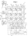
- Figure 1 shows a simplified diagram of a device photosensitive 1, comprising a matrix 2 organized in a conventional manner.
- the matrix 2 comprises photosensitive points P1 to P9, each formed by a photosensitive diode Dp and a switching diode Dc mounted in series following a head-to-tail configuration.
- the matrix includes in-line conductors Y1 to Y3 crossed with column conductors X1 to X3, with at each crossing, a photosensitive point connected between a row conductor and column conductor.
- the photosensitive points P1 to P9 are thus arranged along lines L1 to L3 and columns CL1 to CL3.
- the photosensitive device includes a control circuit line 3, of which outputs SY1, SY2, SY3 are respectively connected to line conductors Y1, Y2, Y3.
- Line 3 control circuit has different elements (not shown), such as for example, circuit clock, switching circuits, shift register, which allow it to perform a sequential addressing of the line conductors Y1 to Y3.
- the photosensitive device further comprises a voltage source 4, delivering to line 3 control circuit a voltage VP used to define the amplitude of pulses applied to the line conductors.
- the two diodes Dp, Dc are connected to each other either by their anode or by their cathode as in the example shown.
- the anode of the photodiode Dp is connected to a column conductor X1 to X3, and the anode of the switching diode Dc is connected to a line conductor Y1 to Y3.
- the two diodes Dp, Dc of each photosensitive point P1 to P9 are polarized conversely, and in this state they each constitute a capacity. He is at note that generally the two diodes Dp, Dc are designed so that the capacitance presented by the photodiode Dp is the strongest (of the order by example of 50 times).
- the line 3 control circuit applies to each line conductor Y1 to Y3 addressed, a so-called read pulse of a given amplitude; the line conductors which are not addressed are maintained at a potential of reference Vr or resting potential, which is mass for example, and which can be the same potential as that applied to column conductors X1 to X3.
- the column conductors X1 to X3 are connected to a circuit CL reading, comprising in the example an integrator circuit 5, and a circuit multiplexer 6 formed for example of an input shift register parallel and serial output can be of the C.C.D type (from the English "Charge Coupled Device ").
- Each column conductor is connected to an input negative "-" of an amplifier G1 to G3 mounted as an integrator.
- a integration capacity C1 to C3 is mounted between the negative input "-” and an output S1 to S3 of each amplifier.
- the second entry "+" of each amplifier G1 to G3 is connected to a potential which in the example is the reference potential Vr, which consequently is imposed on all column conductors X1 to X3.
- Each amplifier has one element switch I1 to I3 called reset (constituted for example by a MOS type transistor), mounted in parallel with each capacitor integration C1 to C3.
- the outputs S1 to S3 of the amplifiers are connected to the inputs And at E3 of the multiplexer 6.
- This conventional arrangement makes it possible to deliver "in series” and line after line, (L1 to L3) at the output SM of the multiplexer 6, signals which correspond to the charges accumulated at points "A" of all photosensitive points P1 to P9.
- FIG. 2 schematically illustrates a photosensitive device 1 ' which differs from that of FIG. 1, mainly in that it comprises a matrix 20 in which the switching diodes Dc, are replaced by transistors T also produced by the deposition techniques of thin film films (TFT).
- TFT thin film films
- the transistor T in each photosensitive point P1 to P9, the transistor T is connected by its source S at the cathode of the photodiode Dp, ie at point "A", its grid G is connected to the line conductor Y1 to Y3 to which the photosensitive point belongs, and its drain D is connected to the column conductor X1 to X3 to which the photosensitive point.
- the anodes of all the Dp photodiodes are combined, and connected to an output SP4 of the line 3 control circuit.
- the output SP4 delivers a voltage called polarization VpL, negative with respect to reference potential VR or mass, of the order for example of -5 volts, which serves to constitute the reverse polarization of the photodiodes Dp; the circuit of line 3 command receives for example this bias voltage from a 4 'power source.
- the line 3 control circuit delivers by its outputs SY1 to SY3, signals or pulses with the same synchronization as in the case of FIG. 1, signals which set the state "passing" simultaneously all the transistors T of the same line L1 to L3.
- Putting a transistor T in the "on” state causes, in each point photosensitive, applying the reference voltage VR to the cathode of the photodiode Dp: from which it results in a way in itself well known, either an initial reverse polarization of the photodiode (in anticipation of a image capture phase); either return to the level of reverse polarization initial (during a reading phase), with circulation in the conductors columns X1 to X3 of a current representing the quantity of charges accumulated in the photosensitive points P1 to P9 belonging to the line L1 to L3 addressed.
- the rest of the operation is similar to that already Explain.
- the proportionality between the value delivered at the output of the multiplexer 6 and the intensity of the useful light signal picked up by a point photosensitive can be altered by various causes, including remanence phenomena are particularly penalizing, due to the fact in particular that they can introduce, when measuring the illumination of a photosensitive point after taking an image, a correlation with the illumination of this same photosensitive point when taking an image previous.
- the most important cause of persistence in the case of matrices whose photosensitive dots are made from materials semiconductor, and even more particularly in the case of silicon amorphous (aSi), resides essentially in a high density of states deep in the band gap of the material: in the case for example of amorphous silicon, the absence of crystal lattice spares traps that can retain charges generated during an image capture. In these conditions the semiconductor material can somehow "memorize" an image corresponding to a given illumination, and restore charges relating to an image during the reading of a next image, or even several following images.
- the invention proposes to produce a current making it possible to fill or saturate the traps (or deep states) present in the structure semiconductor material, so that these traps are then emptied with a statistic that has nothing to do with the previous image, or results a complete absence of correlation and therefore an absence of remanence.
- the invention therefore relates to a method for controlling a photosensitive device comprising a matrix of photosensitive dots, the photosensitive points being arranged in at least one line and at minus one column and each comprising a switch element in series with a common point photodiode, the method consisting of hand to expose the matrix to a light signal said useful during a phase of image capture during which charges produced in each point photosensitive depending on its exposure modify a voltage of polarization of the photodiode, and consisting on the other hand of reading the points photosensitive in a reading phase occurring after the setting phase image, said method being characterized in that it further comprises at least once before the image-taking phase, initially at exposing the photosensitive points of the matrix to a so-called light flux of erasure having an intensity and a duration such as the charges it generates modify the tension of the common points until it reaches the elbow voltage of the photodiodes so as to cause their conduction in the direct direction and then to polarize in reverse all the photodiodes so that the points photosensitive can
- the method of the invention also makes it possible to simple way, to improve the reading efficiency of photosensitive dots, especially when the charges accumulated there are low value.
- a solution to this problem is known by a patent application French n ° 88 12126 published with n ° 2 636 800. This solution applies in the case where the photosensitive points each consist of a photodiode connected in series with a diode acting as an element switch, and with the two diodes mounted in a head-to-tail configuration, as in the example in figure 1.
- This patent application proposes to create by an illumination additional, so-called training loads which are added to each photosensitive point to "signal" charges produced by signal exposure bright useful.
- This additional lighting can be obtained by different types of light source, for example by a lumiplaque or a array of light emitting diodes as decnt in a request for French Patent No. 2,598,250.
- an additional light source SL (symbolized in dotted) can be pressed on the substrate 7, opposite the matrix 1 for do not block the useful light signal.
- the substrate 7 is located in the same plane as that of the figure, the source of light SL is located in a plane deeper than that of the figure.
- the device of Figure 2 can also include such a additional light source (not shown in Figure 2).
- the training charges added to the charges created by the useful light signal minimize the harmful effect (at very low values) produced by the poor qualities of a diode switch used as a switch in the "closed” state, say to the "passing" state. This is due in particular to a non-linearity in the current-voltage characteristic of the diodes, in their conduction mode in the direct direction.
- this solution which uses an optical flash to produce training loads has the disadvantage of also produce significant noise (associated with the optical flash).
- the process of the invention has the advantage of allowing easily add training loads, for the same purpose as that searched in patent application n ° 2 605 166, but by a method electric which generates much lower noise than a method optical.
- Figure 3a represents signals applied to a line conductor Y1 to Y3, the first conductor Y1 for example; and figure 3d represents the variations of a voltage VA at point "A" at floating potential points photosensitive, from the first photosensitive point P1 for example.
- the start of a operation occurs after an instant t1 which marks the end of a pulse IL reading applied to the first line conductor Y1.
- This impulse from IL reading started at time t0 of the start of a PHL reading phase of a previous operating cycle, and it made it possible to read the points photosensitive P1 to P3 exposed during an image capture phase of this previous cycle.
- the reading pulse IL has a positive sign with respect to the voltage of VR reference, and a VP2 amplitude. It puts the switching diode Dc in direct conduction, and this latter charges the capacity which constitutes the photodiode Dp: so that the voltage VA at point "A", in a first step, goes to a value VA1 which corresponds to the voltage of bend of the switching diode Dc and then goes up to a value VA2, substantially equal to VP2 minus the value of the voltage of bend of the switching diode Dc.
- the capacity charge formed by the photodiode Dp causes on the column conductor X1, the circulation of a current corresponding to the charges accumulated at point "A".
- the switching diode Dc is polarized reverse and constitutes a capacitance: the voltage VA at point "A" decreases at a VA3 value per capacitive division.
- a FE luminous flux called "erasing luminous flux” shown in the Figure 3c is applied to all photosensitive points P1 to P9 of the matrix 2, before taking any image.
- the FE erase light flux is applied at all points photosensitive P1 to P9, at an instant t2 which follows the instant t1 'of the end of reading phase of the previous cycle.
- This erasing light flux must have sufficient intensity and duration for the charges it generates, accumulated at points "A” with floating potential, modify the voltage VA at these points "A” (and therefore the polarization of the photodiodes Dp) until putting the photodiodes Dp in conduction in their direct direction.
- the current corresponding to the conduction in the direction direct from the photodiode Dp tends, as previously explained, to saturate the "traps" that exist in the semiconductor material (aSiH for example), and thus tends to "erase” the traces of an image taken previous and avoid any correlation between this image capture previous and an image to come.
- the light source to produce the erasing flux is in itself of a classical type. It can be constituted for example by a light source such as the additional light source SL previously mentioned, i.e. by a lumiplaque or by a array of light emitting diodes, and it can also be arranged against the transparent substrate 7 (FIG. 1) opposite the matrix 2 (note that the light source SL could also be located from the side of matrix 1, provided it does not interfere with the correct exposure of the matrix 2 by the useful light signal, when taking an image).
- the control of the light source SL can be accomplished in a way by itself conventional, for example from a signal delivered by an output Ssl of the line 3 control circuit (figure 1).
- the device photosensitive of Figure 2 can also include a light source SL (not shown in Figure 2), arranged under the same conditions as above explained.
- the method of the invention consists in applying to all line conductors Y1 to Y3, a pulse of so-called IP bias pulse voltage (shown in Figure 3a) having an amplitude VP1, positive with respect to the reference voltage VR, this is at say having the same sign as the reading pulse IL.
- An IP bias pulse can be applied to all line conductors Y1 to Y3 by the line 3 control circuit, i.e. simultaneously to all of these conductors, line by line. What is essential, is that all the line conductors Y1 to Y3 and therefore all photosensitive points P1 to P9, receive the IP polarization pulse before the image taking phase.
- a polarization pulse IP begins (fig. 3a) received by the first line conductor Y1
- the voltage VA at point "A" of all photosensitive points connected to this conductor change sign and goes to the value VA1 which is the elbow voltage of the diode of Dc switching.
- the latter is then returned to direct conduction and the photodiode Dp then having become reverse polarized, its capacity is charged by the switching diode Dc: consequently, the voltage VA increases to reach at an instant t7 when the polarization pulse ceases IP, a value which corresponds to the amplitude Vp1 of this pulse of bias minus the elbow voltage value of the diode Dc switching, in a way that in itself is comparable to that already described for the time interval between time t0 and time t1.
- the process of the invention offers a very important advantage, which lies in the possibility of creating training loads of a simple way, and with high quality (low noise). It suffices for this purpose to give the polarization pulses IP an amplitude VP1 less than the amplitude VP2 of the IL reading pulses
- the voltage VA at point "A” just before an image capture phase has the value VA3 displayed at time t1 (which would be the case if the IP polarization pulse had the same amplitude VP2 as the reading pulse IL), and in supposing on the other hand that this image taking does not provide any illumination of the first photosensitive point P1, and if one does not take account possible drifts and dark currents, the voltage VA at point "A” will have kept the value VA3 after taking the image: consequently, subsequent application of an IL read pulse will not produce the charge of the capacitance formed by the photodiode (when it is polarized in reverse) and no load will be transmitted on the column conductor corresponding, ie the first column conductor X1.
- the amplitude VP1 of the polarization pulse IP is less than that VP2 of the IL reading pulse, at time t7 it gives the voltage VA at point "A" before the image is taken, a value VA5 lower than the value VA3 given by the reading pulse IL: by following we will obtain with the application of an IL reading pulse, a current on the first column conductor X1, current which will represent a so-called training load whose intensity will be proportional to the difference VA3 - VA5.
- the photosensitive device 1 of FIG. 1 may include, in view to create training loads, a second source of tension 13 delivering to the control circuit line 3, a voltage having the value of the amplitude VP1 of the polarization pulse IP; the voltage delivered by the first source 4 having for example the value of the amplitude VP2 of the reading pulse IL.
- the line 3 control circuit can thus, from a in itself known manner, select one or the other of the two voltage and deliver it in the form of pulses to the conductors lines Y1 to Y3 at the appropriate times.
- Training loads can be useful in cases especially low exposure values, especially for photosensitive dots whose switching element is a diode, due to the non-linearity in the current-voltage characteristic in direct mode that has a diode.
- the photosensitive device of FIG. 2 may include also a second voltage source 13 ', applying to the circuit command line 3 a second bias voltage VpP lower than the first bias voltage VpL; line 3 control circuit can thus select between the two voltages VpL and VpP the one that is suitable apply via its output SP4, to the anodes of the photodiodes Dp, depending on whether the "on" state of the transistors T is controlled to accomplish a initial polarization or for a reading phase.
- the voltage VA at point "A” keeps the value VA5 at least until an instant t8, where an image taking phase represented at Figure 3b by a Phi slot. If from time t8 the point photosensitive P1 is subjected to an illumination by a light signal "useful", the charges then produced and accumulated at point "A” cause (as in the example shown in Figure 3d) a decrease of the VA voltage at this point. This decrease is continuous (if the illumination is constant), and it stops at an instant t9 which marks the end of the phase of image capture.
- the voltage VA at point "A” has at this time by example a value VA4 which is kept until an instant t10
- a reading pulse IL is applied to the first conductor line Y1. It marks the beginning of a reading phase PHL used to read the charges produced in the image capture phase PHi.
- the voltage VA goes to the value VA1 with the application of the pulse reading IL; then the switching diode Dc being in driving condition, it charges the capacitance formed by the photodiode Dp which determines a current on the column conductor X1; the voltage VA then increases until its maximum value VA2.
- the voltage VA goes to the value VA3 (as at time t1).
- Read pulses (not shown) are then successively applied to the line conductors Y2, Y3, during the rest of the PHL reading phase, the end of which occurs at an instant t12.
- Figure 3e shows the "open” and “closed” states of reset switches 11, 12, 13, switches that do not allow the integration operation by amplifiers G1, G2, G3 only when they are in the "open” state.
- Figure 3e illustrates the fact that these switches I1 to I3 do not are in the "open” state only during the PHL reading phases, and only by Consequently, only the currents flowing in the conductors column X1 to X3 during the reading phases are taken into account.
- the different time intervals between the instants t1 'and t12 correspond to different stages of a complete sequence of operation of a photosensitive device controlled in accordance with method of the invention.
- the end of the reading phase at time t12 marks the start of a possible next operating sequence.
- the method of the invention is also applicable to the control of photosensitive devices used for image detection radiological.
- These photosensitive devices must then include a scintillator to convert incident radiation including a X-ray, into light radiation in the length band wave to which the photodiodes Dp are sensitive.
- a scintillator can be consisting of a layer 9 (symbolized in FIG. 1 by a square in lines dotted) of a scintillating substance for example in Cesium lodide (Csl); this scintillating layer 9 is deposited over the matrix 2, so as to be interposed between the latter and the incident X-ray.
- the photosensitive device 1 ′ in FIG. 2 can also include a screen scintillator 9 (not shown), arranged in the same manner as that of the Figure 1 device.
- the method of the invention applies from particularly interesting in the case where the scintillator 9 is in Cesium lodide (Csl), because this scintillating substance is known for its very low intrinsic remanence. Pairing a scintillator in Cesium lodide with a matrix 2, 20, whose Dp photodiodes are hydrogenated amorphous silicon (aSiH), under the control of the the invention which eliminates the persistence specific to hydrogenated amorphous silicon, provides very high quality radiological images
Landscapes
- Engineering & Computer Science (AREA)
- Multimedia (AREA)
- Signal Processing (AREA)
- Transforming Light Signals Into Electric Signals (AREA)
- Solid State Image Pick-Up Elements (AREA)
Description
- les figures 1 et 2 représentent des dispositifs photosensibles auxquels peut s'appliquer le procédé de l'invention ;
- les figures 3a à 3e constituent un chronogramme illustrant le fonctionnement des dispositifs des figures 1 et 2, sous la commande du procédé de l'invention.
Claims (24)
- Procédé de commande d'un dispositif photosensible (1, 1') comportant une matrice (2, 20) de points photosensibles (P1 à P9), les points photosensibles étant agencés en au moins une ligne (L1 à L3) et en au moins une colonne (CL1 à CL3) et comprenant chacun un élément interrupteur (Cd, T) en série avec une photodiode (Dp) avec un point commun, le procédé consistant d'une part à exposer la matrice (2, 20) à un signal lumineux dit utile durant une phase de prise d'image (Phi) au cours de laquelle, des charges produites dans chaque point photosensible (P1 à P9) en fonction de son exposition modifient une tension de polarisation (Va3, Va5) de la photodiode (Dp), et consistant d'autre part à lire les points photosensibles dans une phase de lecture (PHL) survenant après la phase de prise d'image (Phi), ledit procédé étant caractérisé en ce qu'il consiste en outre au moins une fois avant la phase de prise d'image (PHi), dans un premier temps à exposer les points photosensibles de la matrice (2, 20) à un flux lumineux dit d'effacement (FE) ayant une intensité et une durée telles que les charges qu'il engendre modifient la tension des points communs jusqu'à ce qu'elle atteigne la tension de coude des photodiodes de manière à provoquer leur mise en conduction dans le sens direct et dans un second temps à polariser en inverse toutes les photodiodes (Dp) de manière à ce que les points photosensibles puissent produire et accumuler les charges au cours de la phase de prise d'image.
- Procédé de commande suivant la revendication 1, caractérisé en ce que l'élément de commutation est une diode dite de commutation (Dc).
- Procédé de commande suivant la revendication précédente, caractérisé en ce que à chaque ligne (L1 à L3) correspond un conducteur ligne (Y1 à Y3) et en ce que à chaque colonne (CL1 à CL3) correspond un conducteur colonne (X1 à X3), et en ce que dans les points photosensibles (P1 à P9) la diode de commutation (Dc) et la photodiode (Dp) sont montées entre un conducteur ligne (Y1 à Y3) et un conducteur colonne (CL1 à CL3) avec des sens de conduction inverses l'une par rapport à l'autre.
- Procédé de commande suivant la revendication précédente, caractérisé en ce qu'il consiste à appliquer à chaque conducteur ligne (Y1 à Y3) une impulsion dite de polarisation (IP) dont le signe correspond à polariser en inverse les photodiodes (Dp), et dont l'amplitude (VP1) détermine la valeur de la polarisation en inverse de ces photodiodes, et en ce que durant la phase de lecture (PHL), il consiste à appliquer à chaque conducteur ligne (Y1 à Y3) une impulsion de lecture (IL) ayant une amplitude (VP2) donnée et un même signe que l'impulsion de polarisation (IP).
- Procédé de commande suivant la revendication précédente, caractérisé en ce que l'impulsion de polarisation (IP) possède une même amplitude que celle (VP2) de l'impulsion de lecture (IL).
- Procédé de commande suivant la revendication 4, caractérisé en ce que l'impulsion de polarisation (IP) possède une amplitude (VP1) inférieure à l'amplitude (VP2) de l'impulsion de lecture (IL).
- Procédé de commande suivant la revendication 1, caractérisé en ce que l'élément de commutation est un transistor (T).
- Procédé de commande suivant la revendication 7, caractérisé en ce que à chaque ligne (L1 à L3) correspond un conducteur ligne (Y1 à Y3) et en ce que à chaque colonne (CL1 à CL3) correspond un conducteur colonne (X1 à X3), et en ce que dans les points photosensibles (P1 à P9), le transistor (T) est relié par sa grille (G) à un conducteur ligne (Y1 à Y3) et par sa source (S) à une première extrémité (cathode ou anode) de la photodiode (Dp) et enfin par son drain (D) à un conducteur colonne (X1 à X3), la seconde extrémité (anode ou cathode) de toutes les photodiodes (Dp) recevant une tension de polarisation (VpP, VpL) permettant de polariser en inverse ces photodiodes.
- Procédé de commande suivant la revendication 8, caractérisé en ce que la valeur de la tension de polarisation (VpP, VpL) est différente suivant qu'elle est appliquée avant une phase de prise d'image (Phi) ou pour une phase de lecture (PHL).
- Procédé de commande suivant l'une des revendications précédentes, caractérisé en ce que au moins les photodiodes (Dp) sont réalisées avec du silicium amorphe hydrogéné (aSiH).
- Procédé de commande suivant l'une des revendications précédentes, caractérisé en ce que la matrice (2,20) est réalisée par des techniques de dépôts en films minces.
- Procédé de commande suivant l'une des revendications précédentes, caractérisé en ce qu'il consiste à réaliser la matrice (2,20) sur un substrat (7) transparent à la lumière.
- Procédé de commande suivant la revendication précédente, caractérisé en ce qu'il consiste à disposer une source de lumière (SL) sur une face du substrat (7) opposée à la face qui porte la matrice (2,20).
- Procédé de commande suivant l'une des revendications précédentes, caractérisé en ce qu'il consiste à interposer un écran scintillateur (9) entre un rayonnement incident et la matrice (2,20).
- Procédé de commande suivant la revendication précédente, caractérisé en ce que le rayonnement incident est un rayonnement X.
- Dispositif photosensible mettant en oeuvre le procédé suivant l'une quelconque des revendications 1 à 15, comportant une matrice (2, 20) de points photosensibles (P1 à P9) agencés en lignes (au moins une ligne) et en colonnes (au moins une colonne), chaque point photosensible étant situé au croisement d'une ligne (L1 à L3) et d'une colonne (CL1 à CL3) et comprenant un élément interrupteur (Cd, T) en série avec une photodiode (Dp), chaque photodiode (Dp) étant polarisée en inverse durant une phase de prise d'image (Phi), la jonction entre une photodiode (Dp) et un élément interrupteur (Cd, T) constituant un point commun (A) à potentiel flottant où sont accumulées des charges produites par la photodiode (Dp), le dispositif photosensible étant caractérisé en ce qu'il comporte des premiers moyens (SL) permettant d'exposer la matrice (2, 20) à un flux lumineux dit d'effacement (FE) ayant une intensité et une durée telles que les charges qu'il engendre modifient la tension des points communs jusqu'à ce qu'elle atteigne la tension de coude des photodiodes de manière à provoquer leur mise en conduction dans le sens direct, et des seconds moyens (3, 13) permettant, après l'application du flux lumineux d'effacement (FE) et avant la phase de prise d'image, de polariser en inverse les photodiodes (Dp) de manière à ce que les points photosensibles puissent produire et accumuler les charges au cours de la phase de prise d'image.
- Dispositif photosensible selon la revendication 16, caractérisé en ce que les seconds moyens (3, 13) permettent d'appliquer à chaque point photosensible (P1 à P9) une impulsion de polarisation ayant un même signe qu'une impulsion de lecture (IL) appliquée aux points photosensibles (P1 à P9) durant une phase de lecture survenant après la phase de prise d'image.
- Dispositif photosensible selon la revendication 17, caractérisé en ce que l'impulsion de polarisation (IP) a une amplitude (VP1) inférieure à l'amplitude (VP2) de l'impulsion de lecture (IL).
- Dispositif photosensible selon la revendication 17, caractérisé en ce que l'impulsion de polarisation (IP) a une amplitude (VP1) égale à celle de l'impulsion de lecture (IL).
- Dispositif photosensible selon l'une des revendications 16 à 19, caractérisé en ce que l'élément interrupteur est un transistor (T).
- Dispositif photosensible selon l'une des revendications 16 à 19, caractérisé en ce que l'élément interrupteur est une diode (Dc).
- Dispositif photosensible selon l'une des revendications 16 à 21, caractérisé en ce que au moins la photodiode (Dp) est réalisée en silicium amorphe hydrogéné (aSiH).
- Dispositif photosensible selon l'une des revendications 16 à 22, caractérisé en ce que, d'une part la matrice (2,20) est réalisée sur un substrat (7) transparent, et d'autre part en ce qu'il comporte une source de lumière (SL) disposée sur une face du substrat opposée à la face qui porte la matrice.
- Dispositif photosensible selon l'une des revendications 16 à 23, caractérisé en ce qu'il comporte un écran scintillateur (9), convertissant un rayonnement X en un rayonnement lumineux dans la bande de longueurs d'onde auxquelles sont sensibles les photodiodes (DP).
Applications Claiming Priority (3)
| Application Number | Priority Date | Filing Date | Title |
|---|---|---|---|
| FR9702752A FR2760585B1 (fr) | 1997-03-07 | 1997-03-07 | Procede de commande d'un dispositif photosensible a faible remanence, et dispositif photosensible mettant en oeuvre le procede |
| FR9702752 | 1997-03-07 | ||
| PCT/FR1998/000450 WO1998041010A1 (fr) | 1997-03-07 | 1998-03-06 | Procede de commande d'un dispositif photosensible a faible remanence, et dispositif photosensible mettant en oeuvre le procede |
Publications (2)
| Publication Number | Publication Date |
|---|---|
| EP0965224A1 EP0965224A1 (fr) | 1999-12-22 |
| EP0965224B1 true EP0965224B1 (fr) | 2004-08-04 |
Family
ID=9504527
Family Applications (1)
| Application Number | Title | Priority Date | Filing Date |
|---|---|---|---|
| EP98913850A Expired - Lifetime EP0965224B1 (fr) | 1997-03-07 | 1998-03-06 | Procede de commande d'un dispositif photosensible a faible remanence, et dispositif photosensible mettant en oeuvre le procede |
Country Status (5)
| Country | Link |
|---|---|
| US (1) | US6686959B1 (fr) |
| EP (1) | EP0965224B1 (fr) |
| DE (1) | DE69825428T2 (fr) |
| FR (1) | FR2760585B1 (fr) |
| WO (1) | WO1998041010A1 (fr) |
Families Citing this family (12)
| Publication number | Priority date | Publication date | Assignee | Title |
|---|---|---|---|---|
| FR2796239B1 (fr) * | 1999-07-06 | 2001-10-05 | Trixell Sas | Procede de commande d'un dispositif photosensible apte a produire des images de bonne qualite |
| FR2817106B1 (fr) * | 2000-11-17 | 2003-03-07 | Trixell Sas | Dispositif photosensible et procede de commande du dispositif photosensible |
| FR2848677B1 (fr) * | 2002-12-17 | 2005-04-15 | Trixell Sas | Detecteur de rayonnement x a l'etat solide |
| JP4144578B2 (ja) * | 2003-10-15 | 2008-09-03 | ソニー株式会社 | 固体撮像装置、画素信号処理方法 |
| FR2861242B1 (fr) | 2003-10-17 | 2006-01-20 | Trixell Sas | Procede de commande d'un dispositif photosensible |
| US7587080B1 (en) | 2004-11-04 | 2009-09-08 | Rockwell Automation Technologies, Inc. | Image retention user interface |
| JP2008017288A (ja) * | 2006-07-07 | 2008-01-24 | Rohm Co Ltd | 光電変換回路及びこれを用いた固体撮像装置 |
| WO2008091975A1 (fr) * | 2007-01-24 | 2008-07-31 | Photodetection Systems, Inc. | Détecteur de rayonnement avec scintillateur à double vitesse |
| FR2942093B1 (fr) | 2009-02-06 | 2011-04-15 | Trixell Sas | Procede de correction d'images obtenues par une matrice de points photosensibles. |
| FR2951311A1 (fr) * | 2009-10-09 | 2011-04-15 | Trixell Sas | Procede de commande d'un dispositif photosensible |
| FR3012934B1 (fr) | 2013-11-04 | 2017-02-24 | Trixell | Detecteur numerique possedant un generateur de lumiere permettant un effacement optique |
| FR3029054B1 (fr) * | 2014-11-24 | 2018-01-26 | Commissariat A L'energie Atomique Et Aux Energies Alternatives | Controle de la duree d'integration dans un dispositif photosensible |
Family Cites Families (16)
| Publication number | Priority date | Publication date | Assignee | Title |
|---|---|---|---|---|
| JPH07105919B2 (ja) * | 1985-06-21 | 1995-11-13 | 株式会社東芝 | 固体撮像装置の駆動方法 |
| FR2593319B1 (fr) * | 1986-01-17 | 1988-03-25 | Thomson Csf | Procede de lecture d'element photosensible constitue d'une photodiode et d'une capacite |
| FR2593343B1 (fr) * | 1986-01-20 | 1988-03-25 | Thomson Csf | Matrice d'elements photosensibles et son procede de fabrication, procede de lecture associe, et application de cette matrice a la prise de vue d'images |
| FR2593987B1 (fr) * | 1986-01-24 | 1989-08-04 | Thomson Csf | Dispositif photosensible a l'etat solide |
| FR2605166B1 (fr) * | 1986-10-09 | 1989-02-10 | Thomson Csf | Dispositif photosensible a l'etat solide, procede de lecture et procede de fabrication |
| US5225706A (en) * | 1987-12-04 | 1993-07-06 | Thomson-Csf | Matrix of photosensitive elements associating a photodiode or a phototransistor and a storage capacitor |
| FR2629932B1 (fr) * | 1988-04-11 | 1991-01-25 | Thomson Csf | Lecteur de documents |
| FR2636800A1 (fr) * | 1988-09-16 | 1990-03-23 | Thomson Csf | Procede de lecture de cellules photosensibles du type comportant deux diodes montees en serie avec des sens de conduction opposes |
| FR2638042A1 (fr) * | 1988-10-14 | 1990-04-20 | Thomson Csf | Procede pour reduire la remanence d'un phototransistor, notamment de type nipin |
| US5093576A (en) * | 1991-03-15 | 1992-03-03 | Cree Research | High sensitivity ultraviolet radiation detector |
| DE4118154A1 (de) * | 1991-06-03 | 1992-12-10 | Philips Patentverwaltung | Anordnung mit einer sensormatrix und einer ruecksetzanordnung |
| US5352884A (en) * | 1993-04-14 | 1994-10-04 | General Electric Corporation | Method and apparatus for providing offset for light detector |
| DE4321789C2 (de) * | 1993-06-30 | 1999-12-09 | Siemens Ag | Festkörperbildwandler |
| GB9404115D0 (en) * | 1994-03-03 | 1994-04-20 | Philips Electronics Uk Ltd | An imaging device |
| FR2731569B1 (fr) | 1995-03-07 | 1997-04-25 | Thomson Tubes Electroniques | Dispositif de recopie de tension a grande linearite |
| FR2759509B1 (fr) | 1997-02-07 | 1999-04-30 | Thomson Tubes Electroniques | Circuit integrateur a linearite amelioree |
-
1997
- 1997-03-07 FR FR9702752A patent/FR2760585B1/fr not_active Expired - Fee Related
-
1998
- 1998-03-06 DE DE69825428T patent/DE69825428T2/de not_active Expired - Lifetime
- 1998-03-06 WO PCT/FR1998/000450 patent/WO1998041010A1/fr not_active Ceased
- 1998-03-06 US US09/367,869 patent/US6686959B1/en not_active Expired - Lifetime
- 1998-03-06 EP EP98913850A patent/EP0965224B1/fr not_active Expired - Lifetime
Also Published As
| Publication number | Publication date |
|---|---|
| FR2760585A1 (fr) | 1998-09-11 |
| WO1998041010A1 (fr) | 1998-09-17 |
| FR2760585B1 (fr) | 1999-05-28 |
| DE69825428T2 (de) | 2005-09-08 |
| EP0965224A1 (fr) | 1999-12-22 |
| US6686959B1 (en) | 2004-02-03 |
| DE69825428D1 (de) | 2004-09-09 |
Similar Documents
| Publication | Publication Date | Title |
|---|---|---|
| EP1378113B1 (fr) | Dispositif photosensible et procede de commande du dispositif photosensible | |
| EP0364314B1 (fr) | Procédé de lecture de cellules photosensibles du type comportant deux diodes montées en série avec des sens de conduction opposés | |
| EP0237365B1 (fr) | Dispositif photosensible | |
| EP0245147A1 (fr) | Panneau de prise de vue radiologique, et procédé de fabrication | |
| EP0233104A1 (fr) | Matrice d'élements photosensibles et son procédé de fabrication, procédé de lecture associé, et application de cette matrice à la prise de vue d'images | |
| FR2629932A1 (fr) | Lecteur de documents | |
| FR2638286A1 (fr) | Dispositif photosensible du type a amplification du signal au niveau des points photosensibles | |
| EP0965224A1 (fr) | Procede de commande d'un dispositif photosensible a faible remanence, et dispositif photosensible mettant en oeuvre le procede | |
| EP0324677B1 (fr) | Matrice photosensible à trois diodes par point, sans remise à niveau | |
| EP0331546B1 (fr) | Matrice photosensible à deux diodes par point, sans conducteur spécifique de remise à niveau | |
| CA2539506C (fr) | Procede de commande d'un dispositif photosensible | |
| CA2378444C (fr) | Procede de commande d'un dispositif photosensible apte a produire des images de bonne qualite | |
| CA2449939C (fr) | Procede de commande d'un dispositif photosensible | |
| EP0357468B1 (fr) | Matrice photosensible à deux diodes de même polarité et une capacité par point photosensible | |
| EP0378593A1 (fr) | Dispositif de visualisation et d'ecriture | |
| FR2762741A1 (fr) | Procede de commande d'un detecteur d'image offrant une protection contre les eblouissements, et detecteur d'image mettant en oeuvre le procede | |
| FR2770954A1 (fr) | Procede de commande d'un detecteur d'image numerique a faible remanence, et detecteur d'image mettant en oeuvre le procede | |
| EP0275740A1 (fr) | Circuit de lecture d'un dispositif photosensible à transfert de ligne, dispositif photosensible à transfert de ligne comportant un tel circuit, et procédé de lecture d'un tel dispositif |
Legal Events
| Date | Code | Title | Description |
|---|---|---|---|
| PUAI | Public reference made under article 153(3) epc to a published international application that has entered the european phase |
Free format text: ORIGINAL CODE: 0009012 |
|
| 17P | Request for examination filed |
Effective date: 19990824 |
|
| AK | Designated contracting states |
Kind code of ref document: A1 Designated state(s): DE FR |
|
| 17Q | First examination report despatched |
Effective date: 20030915 |
|
| GRAP | Despatch of communication of intention to grant a patent |
Free format text: ORIGINAL CODE: EPIDOSNIGR1 |
|
| GRAS | Grant fee paid |
Free format text: ORIGINAL CODE: EPIDOSNIGR3 |
|
| RAP1 | Party data changed (applicant data changed or rights of an application transferred) |
Owner name: THALES ELECTRON DEVICES S.A. |
|
| GRAA | (expected) grant |
Free format text: ORIGINAL CODE: 0009210 |
|
| AK | Designated contracting states |
Kind code of ref document: B1 Designated state(s): DE FR |
|
| REF | Corresponds to: |
Ref document number: 69825428 Country of ref document: DE Date of ref document: 20040909 Kind code of ref document: P |
|
| PLBE | No opposition filed within time limit |
Free format text: ORIGINAL CODE: 0009261 |
|
| STAA | Information on the status of an ep patent application or granted ep patent |
Free format text: STATUS: NO OPPOSITION FILED WITHIN TIME LIMIT |
|
| 26N | No opposition filed |
Effective date: 20050506 |
|
| REG | Reference to a national code |
Ref country code: FR Ref legal event code: PLFP Year of fee payment: 19 |
|
| REG | Reference to a national code |
Ref country code: FR Ref legal event code: PLFP Year of fee payment: 20 |
|
| PGFP | Annual fee paid to national office [announced via postgrant information from national office to epo] |
Ref country code: FR Payment date: 20170227 Year of fee payment: 20 Ref country code: DE Payment date: 20170228 Year of fee payment: 20 |
|
| REG | Reference to a national code |
Ref country code: DE Ref legal event code: R071 Ref document number: 69825428 Country of ref document: DE |