EP0964508B1 - Circuit arrangement for feeding an electric motor - Google Patents
Circuit arrangement for feeding an electric motor Download PDFInfo
- Publication number
- EP0964508B1 EP0964508B1 EP99201758A EP99201758A EP0964508B1 EP 0964508 B1 EP0964508 B1 EP 0964508B1 EP 99201758 A EP99201758 A EP 99201758A EP 99201758 A EP99201758 A EP 99201758A EP 0964508 B1 EP0964508 B1 EP 0964508B1
- Authority
- EP
- European Patent Office
- Prior art keywords
- circuit
- signal
- commutation
- circuit arrangement
- input
- Prior art date
- Legal status (The legal status is an assumption and is not a legal conclusion. Google has not performed a legal analysis and makes no representation as to the accuracy of the status listed.)
- Expired - Lifetime
Links
- 238000004804 winding Methods 0.000 claims description 18
- 238000005070 sampling Methods 0.000 claims description 15
- 238000005259 measurement Methods 0.000 claims description 13
- 230000001419 dependent effect Effects 0.000 claims description 6
- 230000004913 activation Effects 0.000 claims 1
- 230000000306 recurrent effect Effects 0.000 claims 1
- 108010076504 Protein Sorting Signals Proteins 0.000 description 23
- 238000001514 detection method Methods 0.000 description 6
- 238000000034 method Methods 0.000 description 6
- 230000000875 corresponding effect Effects 0.000 description 5
- 238000007493 shaping process Methods 0.000 description 5
- 238000012935 Averaging Methods 0.000 description 3
- 239000003990 capacitor Substances 0.000 description 3
- 238000010586 diagram Methods 0.000 description 3
- 230000000694 effects Effects 0.000 description 3
- 230000001960 triggered effect Effects 0.000 description 3
- 238000003079 width control Methods 0.000 description 3
- 230000001276 controlling effect Effects 0.000 description 2
- 230000003071 parasitic effect Effects 0.000 description 2
- 230000001360 synchronised effect Effects 0.000 description 2
- 238000012546 transfer Methods 0.000 description 2
- 206010027336 Menstruation delayed Diseases 0.000 description 1
- 230000033228 biological regulation Effects 0.000 description 1
- 230000002596 correlated effect Effects 0.000 description 1
- 230000007423 decrease Effects 0.000 description 1
- 230000003247 decreasing effect Effects 0.000 description 1
- 230000003111 delayed effect Effects 0.000 description 1
- 238000013461 design Methods 0.000 description 1
- 238000011161 development Methods 0.000 description 1
- 238000011156 evaluation Methods 0.000 description 1
- 230000005415 magnetization Effects 0.000 description 1
- 238000012986 modification Methods 0.000 description 1
- 230000004048 modification Effects 0.000 description 1
- 230000002265 prevention Effects 0.000 description 1
- 230000010349 pulsation Effects 0.000 description 1
- 230000001105 regulatory effect Effects 0.000 description 1
- 238000010079 rubber tapping Methods 0.000 description 1
- 230000002123 temporal effect Effects 0.000 description 1
Images

Classifications
-
- H—ELECTRICITY
- H02—GENERATION; CONVERSION OR DISTRIBUTION OF ELECTRIC POWER
- H02P—CONTROL OR REGULATION OF ELECTRIC MOTORS, ELECTRIC GENERATORS OR DYNAMO-ELECTRIC CONVERTERS; CONTROLLING TRANSFORMERS, REACTORS OR CHOKE COILS
- H02P6/00—Arrangements for controlling synchronous motors or other dynamo-electric motors using electronic commutation dependent on the rotor position; Electronic commutators therefor
- H02P6/14—Electronic commutators
- H02P6/16—Circuit arrangements for detecting position
- H02P6/18—Circuit arrangements for detecting position without separate position detecting elements
- H02P6/185—Circuit arrangements for detecting position without separate position detecting elements using inductance sensing, e.g. pulse excitation
-
- H—ELECTRICITY
- H02—GENERATION; CONVERSION OR DISTRIBUTION OF ELECTRIC POWER
- H02P—CONTROL OR REGULATION OF ELECTRIC MOTORS, ELECTRIC GENERATORS OR DYNAMO-ELECTRIC CONVERTERS; CONTROLLING TRANSFORMERS, REACTORS OR CHOKE COILS
- H02P27/00—Arrangements or methods for the control of AC motors characterised by the kind of supply voltage
- H02P27/04—Arrangements or methods for the control of AC motors characterised by the kind of supply voltage using variable-frequency supply voltage, e.g. inverter or converter supply voltage
- H02P27/06—Arrangements or methods for the control of AC motors characterised by the kind of supply voltage using variable-frequency supply voltage, e.g. inverter or converter supply voltage using dc to ac converters or inverters
-
- H—ELECTRICITY
- H02—GENERATION; CONVERSION OR DISTRIBUTION OF ELECTRIC POWER
- H02P—CONTROL OR REGULATION OF ELECTRIC MOTORS, ELECTRIC GENERATORS OR DYNAMO-ELECTRIC CONVERTERS; CONTROLLING TRANSFORMERS, REACTORS OR CHOKE COILS
- H02P6/00—Arrangements for controlling synchronous motors or other dynamo-electric motors using electronic commutation dependent on the rotor position; Electronic commutators therefor
- H02P6/14—Electronic commutators
Definitions
- the invention relates to a circuit arrangement for dining a Electric motor with at least three windings from a DC voltage source a commutation circuit, each to a winding connection of the Electric motor a commutation branch with a first and a second Includes switch element through which the winding connection in question optionally with a first connection of the DC voltage source or via a measuring impedance a second connection of the DC voltage source can be connected to a ring counting device for periodically reversing the switch elements of the Commutation circuit according to a clock signal in the Ring counting device rotating signal sequence, with a period of Ring counting device a complete circulation of the signal sequence in the Ring counting device corresponds, and with a clock frequency generation stage Output of the clock signal, which is a clock frequency dependent on the measuring voltage having.
- Position measuring elements in particular Hall elements, for the movable armature of the engine. Since these position measuring elements are arranged stationary are the angle between the armature voltage and the electromotive force (EMF) of the motor under all loads. In addition, such Position measuring elements of simplification and miniaturization electronically commutated DC motors undesirable limits.
- EP 0 156 282 A1 describes a method and an arrangement for control a brushless AC motor known by a so-called Inverter circuit is operated, which is connected to a DC voltage source is.
- the direct current supplied to the inverter circuit is measured. That from this Measurement resulting measurement signal is on the one hand in a peak value detector for processes the detection of positive current peaks into a peak signal which a first controller for generating a frequency control signal is supplied. This control decreases the value of the frequency control signal when the peak of the motor current exceeds a predetermined value.
- Frequency control signal is a clock signal via a voltage-controlled oscillator generated, the frequency of which via a frequency divider and a ring counter Basis for the commutation of the AC motor via the Inverter circuit forms. From the measurement signal, which from the motor current is obtained, an average is also formed and the so generated Average signal divided by the frequency control signal by one Obtain speed request signal. In addition, the measurement signal in a second peak detector on the negative current peaks of the motor current corresponding second voltage control signal is formed, which is a measure of the Magnetization of the motor should represent. From the difference of the Speed request signal and the second voltage control signal become one Pulse width control signal derived.
- a pulse width control stage with this pulse width control signal, the pulse widths of the clock signal from voltage controlled oscillator controlled.
- the Peak signal from the first peak detector (positive current peaks) supplied is also provided with a control input, that of a Speed request input via a ramp generator Ramp signal is supplied.
- This ramp signal is in the start-up phase and the braking phase the value of the frequency control signal is lowered, whereby the voltage controlled oscillator in startup mode a gradually increasing Frequency and generates a gradually decreasing frequency in braking mode.
- the engine speed follows one by a fixed one Voltage regardless of the load and the operating state of the engine predetermined frequency. If the engine speed drops at this frequency, this operating state is caused by an increase in the motor current over a predetermined limit value is also detected. It will then go according to a given Time course a gradually increasing from a low value to the final value Frequency specified to give the motor the opportunity to restart. There is no regulation based on the measured motor current.
- DE 37 12 185 includes a load current detection device for converters Pulse duration modulation known.
- a converter has several arms in parallel to a DC voltage source. Each arm is made up of an upper arm and one formed lower arm, each having a switching element. The switching elements the upper arm and lower arm, respectively, become continuous and alternately supplied switching control signals. Shunt resistances are between a negative connection of the DC voltage source and the switching elements of the lower arms turned on.
- the power converter also has a desired current waveform generator circuit, the guide values for the infeed generates current waveforms desired in a load, one Carrier vibration generator and sample and hold circuits.
- Each of the sampling and Holding circuits sense one at the respective shunt resistor falling voltage in synchronism with the period of that Carrier vibration generator generated carrier vibration at a certain Time during the period during which the assigned switching element is conductive, and holds this voltage.
- There is one Reference value signal generator circuit is provided which supplies a reference value signal. This is compared with the output signal of the Carrier vibration generator compared. Exceeds the output signal of the Carrier vibration generator the output signal of the Reference signal generator circuit, i.e. the reference signal, the sampled signals held in the sample and hold circuits.
- From European patent 231 046 is a commutation circuit for one brushless DC motor without a commutation sensor known to one Stand with a multi-phase system and a permanent magnetic rotor.
- the commutation state of the motor is dependent on that in the stator windings induced voltages. It becomes a comparison signal generated, which indicates whether the sign of that winding voltage that is not is connected to the direct current source by means of the electronic switching elements, with a given depending on the respective commutation state Sign matches.
- This comparison signal is hidden during the times in which in the windings by switching off the electronic Compensating processes caused by switching elements with possible parasitic zeros occur.
- the switching elements always become a commutation step switched on if the comparison signal does not match the sign indicates.
- Voltage-dependent commutation is an alternative to current-dependent commutation, which is not always desired.
- the time of detection of the output current of the PWM inverter by a pulse width modulated Signal is controlled, which is obtained by comparing a Output voltage control signal or a modulation signal with a triangular carrier signal, is placed near the point in time which is opposite the Time at which the triangular carrier signal reaches its maximum amplitude by one Delayed period that is half as long as the entire duration of the switch-on delay time driver transistors used as switch elements of the PWM inverter, their turn-off delay time and a short-circuit prevention period of the upper and lower branches of the PWM inverter.
- the current value almost in the middle between turning points of a pulse component in the output current of the PWM inverter is detected and can almost be the basic component of the output current of the PWM inverter can be detected.
- the invention has for its object a circuit arrangement for dining a To create an electric motor that commutation depending on the motor current without position elements, which is reliable with little circuitry trained for all operating conditions of the engine, in particular all speeds is.
- this object is achieved with a circuit arrangement of the generic type Kind solved in that with the measuring impedance an input of a Sample and hold circuit is coupled to sample one at the measuring impedance occurring measuring voltage and that the sample and hold circuit by the ring counting device in each of its periods at a predetermined time outside the time intervals for reversing the switch elements of the commutation circuit driven to take a sample of the measuring voltage becomes.
- the invention is based on the knowledge that instead of one, if appropriate difficult to get average motor current also one to one suitably selected moment sampled instantaneous value of the motor current Can provide information about the load on the engine. It turns out that the Motor current at the commutation points, i.e. at the time when the Switch elements of the commutation branches are switched because of these switching operations occurring in the windings of the electric motor and not a reliable one due to asymmetries in the commutation circuit Can give information about the load on the engine and thus at these times must not be measured. Outside the temporal sphere of influence of the above However, an instantaneous value of the motor current can be found as a disturbing factor is at least almost proportional to the load on the engine.
- a good Sampling point in time at which the instantaneous value of the motor current exceeds the above Requirements fulfilled lies in the middle of a commutation interval.
- a particularly simple circuit arrangement for determining the above Sampling times are obtained in that the ring counting device as Shift register is formed and has a number of register cells that at least twice the number of switch elements of the commutation circuit equivalent. If twice as many register cells as switch elements are selected, can the sampling times by simply selecting which of the Register cells the sampling is to be triggered, on the middle between two Commutation times can be set. Provide these commutation times represents the beginning of the time intervals for reversing the switch elements If a higher number of register cells is selected, the sampling times, i.e. the times for taking a sample of the measuring voltage, without large Switching effort to another point between two Commutation times can be determined.
- a time period between two consecutive times Reversing operations of the switch elements of the commutation circuit, i.e. on Period between two successive commutation times, at least two periods of the clock signal, and driving the sampling and Hold circuit is indicated by an edge of the clock signal within the Period triggered.
- the most general design is Ring counting device every nth of its register cells with one of the switch elements connected to the commutation circuit, where n is the quotient of the number of all Register cells of the ring counter and the number of switch elements.
- On Sampling signal for triggering a sampling process in the sample and hold circuit is derived from a register cell, which is located in the shift register between two successive, each with one of the switch elements of the Commutation circuit connected register cells is located.
- the circuit arrangement For deriving a pulse-shaped scanning signal from the ring counting device the circuit arrangement according to the invention preferably contains one Pulse shaping stage.
- the scanning signal thereby receives one of the operating status of the electric motor independent time course.
- the circuit arrangement according to the invention can only be used little effort with an input circuit for storing at least one predeterminable signal sequence and for entering this signal sequence, preferably for Enter this signal sequence once into the ring counting device Commissioning of the circuit arrangement.
- you turn on the Electric motors can from such an input circuit in the Ring counting device differently predeterminable signal sequences, i.e. different Switching status pattern for the register cells of the ring counting device, fed through which an operation with different commutation behavior of the Electric motor is possible.
- the current flow angle for the Windings of the electric motor can be selected.
- the circuit arrangement according to the invention can also be used for a simple manner Speed control of the connected electric motor can be used.
- a control stage for regulating the speed of the electric motor to a specifiable Value connected to the control stage as a current setpoint.
- the control level contains a comparison arrangement for forming a comparison signal Compare the current setpoint with the sample values of the measuring voltage.
- the Comparison signal is used to derive the clock signal of the clock frequency generation stage fed.
- the circuit arrangement according to the invention is preferred for simply constructed electric drives with electronically commutated electric motors can be used.
- On Preferred areas of application for such electric motors are household appliances, for example electric shavers.
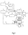
- the block diagram of the first embodiment of the invention 1 includes an example formed with three windings Electric motor 1 from a DC voltage source 2, for example one Battery or an accumulator, is fed and with this via a Commutation circuit 3 is connected.
- the circuit elements and Line connections that serve to supply energy to the electric motor 1 stronger solid lines compared to the circuit elements and connections highlighted that the signal, i.e. the transfer of information in which serve circuit arrangement according to the invention.
- one Measuring impedance 4 preferably an ohmic resistance with low Resistance value, inserted.
- a connection point between the DC voltage source 2 and measuring impedance 4 are connected to ground 12.
- the winding connections 13, 14 or 15 of the electric motor 1 optionally with the first connection of the DC voltage source - here positive pole of the battery - or via the measuring impedance 4 connected to the second connection of the DC voltage source - here negative pole become. In operation of the electric motor, this happens at predetermined times or at predetermined time intervals in such a way that the anchor of the Electric motor is rotated.
- the commutation circuit 3 To control the necessary for this commutation of the electric motor 1 Switching operations is the commutation circuit 3 via switching lines 16 to 21 with a ring counter 5 connected.
- the ring counter 5 is one Clock frequency generation stage 7 is supplied with a clock signal through which a Predeterminable signal sequence is clocked in the ring counting device 5.
- a Period of the ring counting device 5 corresponds to a complete revolution of the mentioned signal sequence in the ring counting device 5 or one revolution of the Rotor of the electric motor 1.
- the clock signal is generated by the clock frequency generation stage 7 via a clock line 22 to the ring counting device 5 transfer.
- the embodiment of FIG. 1 also includes a scanning and Holding circuit 6, via a measured value line 23 with that of the connection with Ground 12 facing away from the measuring impedance 4 is connected. About the Measured value line 23 becomes the measuring voltage occurring at the measuring impedance 4 Sample and hold circuit 6 fed.
- the sample and hold circuit 6 is also connected to the ring counting device 5 via a pulse shaping stage 8. Like in will be explained in more detail below, is via a line 24 the ring counter 5 at a suitable position with the signals on the Switching lines 16 to 21 or correlated with the signal on the clock line 22 Tapped signal. This signal is used in the pulse shaping stage 8 shaped pulse-shaped scanning signal and a scanning signal line 25 to the Sample and hold circuit 6 forwarded. When a pulse occurs in this sampling signal is the instantaneous value of the measuring voltage on the Measured value line 23 sampled in the sample and hold circuit 6 and for further evaluation saved.
- the value of the measuring voltage stored in the sample and hold circuit 6 becomes fed via a further line 26 to the clock frequency generation stage 7 to control the clock frequency depending on the value of the measuring voltage.
- a control loop for commutation of the Electric motor 1 closed.
- a current setpoint - preferably in the form of a DC voltage - can be output.
- This current setpoint occurs via a line a setpoint input 28 of a comparison arrangement 10
- the actual value input 29 of the measurement voltage from line 26 stored in the sample and hold circuit 6 is fed.
- a Switchover signal From the output 30 of the comparison arrangement 10 is a Switchover signal, which has a value corresponding to the comparison result assumes a control input 31 of a changeover stage 32.
- the Switching stage 32 is corresponding to the signal at its control input 31 switched that the clock frequency generation stage 7 optionally the current setpoint supplied via line 27 or the measuring voltage via line 26 become.
- the switching stage 32 is in that shown in Fig. 1 Switch position in which the connection between the sample and hold circuit 6 and the clock frequency generation stage 7 is established.
- the circuit arrangement according to FIG. 1 also contains an input circuit 9 which at an input 33 the signal from the clock line 22 is supplied and the latter Output 34 connected to a further input 35 of the ring counting device 5 is. At least one predeterminable signal sequence is stored in the input circuit.
- this signal sequence With the help of the signal on the Clock line 22 loaded into the ring counter 5.
- By optional charging different signal sequences stored in the input circuit 9 different torque-speed dependencies for the operation of the Electric motor 1 can be specified. This is shown in the exemplary embodiments of FIG 3 and 4 explained in more detail.
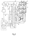
- Fig. 2 shows a further embodiment of the invention Circuit arrangements in which the commutation circuit 3 and Ring counting device 5 are shown in more detail.
- For simplification 2 does not contain a control stage 10, 11, 32, and the input circuit with the reference symbol 90 in FIG. 2 is simplified played.
- the commutation circuit 3 points to each of the winding connections 13, 14, 15 of the electric motor 1 a commutation branch 36, 37 and 38 respectively.
- Each of the commutation branches 36, 37 and 38 is between a first one Connection 39 of the DC voltage source 2 - here the positive pole - and via the Measuring impedance 4 with the second connection 40 of the DC voltage source 2 - here the negative pole - and ground 12 connected.
- Each of the commutation branches 36, 37, 38 comprises a first switch element through which the winding connection 13, 14 or 15 connected to the first terminal 39 of the DC voltage source 2 can be.
- Each of these first switch elements of the commutation branches 36, 37, 38 comprises the parallel connection of a pnp transistor with a free-wheeling diode.
- the commutation branches 36, 37, 38 each contain a second one Switch element for connecting the winding connections 13, 14 and 15 with the second connection 40 of the DC voltage source 2 via the measuring impedance 4, wherein these second switch elements each with the parallel connection of an NPN transistor another freewheeling diode.
- the ring counting device 5 in FIG. 2 is designed with a shift register 50, which has a number of register cells that is twice the number of Switch elements of the commutation circuit 3 corresponds, i.e. there are twelve Register cells available.
- a signal sequence stored in these register cells is in the by a clock signal at a common clock signal input 51 Register cells clocked all round, for which purpose an output 52 of the last of the Register cells is connected to an input 53 of the first of the register cells.
- the clock signal input 51 of the shift register 50 is connected to the clock line 22 connected.
- the output 34 of the input circuit 90 in 2 includes a connection to shift register 50 for each of the register cells; accordingly, shift register 50 includes one for each of its register cells Connection of the input 35.
- shift register 50 includes one for each of its register cells Connection of the input 35.
- a binary signal value corresponding to one of the possible switching states of the register cells of the shift register 50 can be specified. This is between the schematic representation of a mechanical switch positive and negative potential (mass) indicated.
- the selectable signal sequence can be loaded into the shift register 50 by the input circuit 90. On In this way, different commutation sequences for the electric motor 1 can be set to different torque-speed dependencies to lead. Thus, the modes of operation of the electric motor 1 are through the setting different signal sequences variable.
- every second one of the register cells has an output to one the switching lines 16 to 21 connected.
- an exit is the first Register cell to the switching line 16 for the second switch element of the Commutation branch 36 connected.
- An output of the fifth register cell leads to the switching line 17 for the second switch element of the Commutation branch 37, an output of the ninth register cell is on the Switching line 18 for the second switch element of the commutation branch 38 connected.
- Outputs of the first, second and third inverters 54, 55, 56 are to the first Switch elements of the commutation branches 36, 37 and 38 guided. To this In this way, the signals from the outputs of the register cells become immediate second switch elements and in inverted form the first switch elements of Commutation circuit 3 fed. In this type of shift register 50 still corresponds to a period between two consecutive Reversing operations of the switch elements of the commutation circuit 3 two Periods of the clock signal on the clock line 22.
- the commutation of the electric motor 1 can thereby be refined or further varied that the number of register cells of the shift register 50 is n times that Number of switch elements corresponds, where n is an integer greater than 2.
- n is the quotient of the number of register cells and the number of switch elements
- every nth register cell of the Ring counting device 5 is one of the switch elements Commutation circuit 3 connected.
- the scanning signal for triggering a Sampling process in the sample and hold circuit 6 is then one of the Register cells derived, which are in the shift register between two on top of each other following the one with each of the switch elements of the commutation circuit 3 connected register cells.
- Shift registers can be the time for the scan between two Reversing operations of the switch elements of the commutation circuit 3 selected differently and thus possibly in the Commutation circuit occurring operations are adjusted.
- Fig. 3 shows a variation of the embodiment of FIG. 2, in which the Input circuit 90 is supplemented by a start circuit 60.
- a Input circuit 9 according to FIG. 1 could preferably input circuit 90 of FIG 2 and 3 may be included together with the start circuit 60.
- the Start circuit 60 is used to control the input of the predefinable signal sequence in the shift register 50 when starting up the electric motor 1 or the latter controlling circuit arrangement according to Fig. 3.
- the start circuit 60 includes a power-on reset generator 61 and a counting device 62.
- the power-on reset generator 61 gives one when switching on the power supply Switch-on reset pulse and is during the remaining operating time Circuit arrangement with no further effect. Via a reset line 63 is with this switch-on reset pulse, both the shift register 50 and the Counter 62 reset to an initial state.
- the Circuit arrangement By switching on the power supply to the other parts of the Circuit arrangement shown, in particular also to the clock frequency generation stage 7 and the commutation circuit 3, the Circuit arrangement put into operation insofar as the clock frequency generation stage 7 outputs 22 clock pulses via the clock line.
- the counting device 62 Through this Clock pulses via a connection to the clock line 22 to the Counting device 62 arrive, the counting device 62 is out of it Starting state clocked in a predeterminable final counting state and in this for the further duration of operation of the electric motor recorded.
- the The final counting state is determined by the counting device 62 via a Input control line 64 given an input signal to the shift register 50 by that the signal sequence specified in the input circuit 90 via the input 35 in the shift register 50 is loaded.
- With the further clock pulses on the Clock line 22 then becomes this predetermined signal sequence in shift register 50 begin to circulate in a ring and the desired commutation of the Effect electric motor 1.
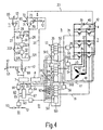
- the ring counting device 5 comprises three Shift registers 501, 502, 503, each with a third of the total number of Register cells.
- the register cells of all shift registers 501, 502, 503 are for that Circulation of the predetermined signal sequence connected in series in the same way like the register cells of the shift register 50 of the exemplary embodiments according to FIG. 2 or 3.
- the interconnection of the shift registers 501, 502, 503 with the same effect as shift register 50 Via clock signal inputs 511, 512 or 513, shift registers 501, 502, 503 become synchronous from clock line 22 clocked.
- the exemplary embodiment according to FIG. 4 comprises an input circuit 91, which contains on the one hand the start circuit 60 and on the other hand a simplified embodiment of the input circuit designated by the reference symbol 90 in FIGS. 2 and 3.
- This simplified input circuit 91 of FIG. 4 is set up for optionally specifying two different signal sequences in the shift registers 501, 502, 503.
- connections of the input 35 of the ring counting device 5 for the individual register cells are connected in the following way:
- the connections for the first shift register 501 are connected via series resistors 92 to a positive supply voltage connection 93; accordingly, the connections of the input 35 for the third shift register 503 are connected directly to ground 12; the connections of the input 35 of the last two register cells of the second shift register 502 are also permanently connected to ground 12; the connections of the input 35 for the first two register cells of the second shift register 502 are connected to one another and to a changeover switch 94, by means of which they can be connected either to ground 12 or to the positive supply voltage connection 93 via a series resistor 95. Switching by means of the switch 94 sets the two different signal sequences.
- the power-on reset generator 61 in the start circuit 60 within the Input circuit 91 comprises a series connection of a resistor and one Capacitor between the positive supply voltage connection 93 and ground 12.
- the switch-on reset generator is simplifying in the present exemplary embodiment 61 with the same positive supply voltage connection 93 connected like the series resistors 92, 95.
- the latter can also be connected to one of the Voltage of the positive supply voltage terminal 93 derived Reference potential. This also applies to the others below Connections to the positive supply voltage connection 93, which will be explained later.
- a tap between the resistor and the capacitor in the power-on reset generator 61 is connected to the reset line 63 via an inverter. In this way, the potential increases when the circuit arrangement is started up on the reset line 63 first a high and after reloading the Capacitor permanently low.
- the counting device 62 has its reset input on the reset line 63 and with a count input 65 to the output of a NAND gate 66 connected.
- One input of NAND gate 66 is on clock line 22 connected, another input of the NAND gate 66 is connected to the Input control line 64 connected. This in turn is connected to an inverter a counting output 67 of the counting device 22 is connected, at which predetermined counter position of the counting device 62 a positive Voltage potential occurs.
- the counting device 62 When the circuit arrangement is started up, the counting device 62 is first reset by power-on reset generator 61 and then by pulses on the Clock line 22 clocked up to the counter position at which the count output 67 Voltage potential changes. This makes another one via the NAND gate 66 Advancing of the counter 62 prevented. At the same time it will Input signal formed on the input control line and to the shift registers 501, 502, 503 given. In their register cells, the according to the selected signal sequence, predetermined voltage potentials are loaded. As in Fig. 3 the starting circuit 60 ineffective in the following.
- the sample and hold circuit 6 in the embodiment of FIG. 4 includes one Operational amplifier 70, the non-inverting input on the one hand via a Storage capacity 71 with the positive supply voltage connection 93 and on the other hand via an analog switch 72 with the measured value line 23 for feeding the Measuring voltage from the measuring impedance 4 is connected.
- the analog switch 72 is Controlled by the scanning signal via the scanning signal line 25, i.e. at his Occurrence switched on; the rest of the time, the analog switch is 72 blocked.
- the inverting input of operational amplifier 70 is via a adjustable voltage divider 73 connected to ground 12. A tap of the adjustable voltage divider is connected to the output of operational amplifier 70 connected for feedback.
- the comparison arrangement 10 comprised by the control stage is one formed another operational amplifier, the inverting input of the Setpoint input 28 and its non-inverting input the actual value input 29 form the comparison arrangement 10.
- the inputs 28, 29 are each one Series resistor connected to line 27 or 26, with line 26 for the value of the measuring voltage from the sample and hold circuit 6 with the output of the operational amplifier 70 is connected and the line 27 for the current setpoint representing DC voltage with the output of a third Operational amplifier is connected, which forms the setpoint adjuster 11.
- the the Operational amplifier forming setpoint adjuster 11 is connected to its output inverting input fed back. Its non-inverting input is on Tapping a potentiometer, the end connections of which with the positive Supply voltage connection 93 or ground 12 are connected. About this The current setpoint can be specified using the potentiometer.
- the switching stage 32 in Fig. 4 comprises a first switch 321, through which the Line 26 for the value of the measuring voltage with a node 325 can be connected. Via a second switch 322, the line 27 for the DC voltage representing the current setpoint also with the Node 325 are connected.
- a first inverter 323 is with its Input connected to the output 30 of the comparison arrangement 10 and via its output connected to the input of a second inverter 324.
- the output of the second inverter 324 is a control input 311 of the first switch 321, a control input 312 of the second switch 322 at the output of the first inverter 323 connected. In this way, the switches 321, 322 are reversed by the Switched signal at the output 30 of the comparison arrangement 10.
- Switching the Switching stage 32 is carried out by comparing the value of the measuring voltage and the value of the DC voltage representing the current setpoint in the Way that the measuring voltage is supplied to node 325, so long this is greater than the value of the current setpoint DC. If, on the other hand, the setpoint is greater than the measuring voltage, the second switch 322 closed and the first switch 321 opened, so that the Node 325 only the setpoint is supplied.
- FIG. 4 there is between the switching stage 32 and the clock frequency generation stage 7 a fourth operational amplifier inserted, the inverting input via a Series resistor is connected to node 325 and its output on the input of the clock frequency generation stage 7 is performed, through which this controlling voltage is supplied.
- the exit of this fourth Operational amplifier with reference numeral 80 is adjustable Resistor fed back to its inverting input. From inverting Input also connects to the tap via a series resistor another potentiometer, the end connections of which with the positive Supply voltage connection 93 or ground 12 are connected. The non-inverting The input of the fourth operational amplifier 80 is connected to ground 12.
- the between ground 12 and the positive supply voltage terminal 93 connected potentiometer in the wiring of the fourth Operational amplifier 80 and the setpoint adjuster 11 can optionally also be used one of their connections to one instead of the positive supply voltage connection Connection can be made via which a suitably selectable reference voltage can be delivered.
- One of the outputs of the fourth register cell of shift register 501 leads Connection to an input of the first register cell of shift register 502 also the line 24 to the pulse shaping stage 8, preferably as a monostable Multivibrator is running.
- the length of time of this monostable Multivibrator output pulse - following a selected switching edge in the Output signal of the fourth register cell of shift register 501 - is selected that a defined reloading of the storage capacity 71 can take place.
Description
Die Erfindung bezieht sich auf eine Schaltungsanordnung zum Speisen eines Elektromotors mit wenigstens drei Wicklungen aus einer Gleichspannungsquelle über eine Kommutierungsschaltung, die zu je einem Wicklungsanschluß des Elektromotors einen Kommutierungszweig mit einem ersten und einem zweiten Schalterelement umfaßt, durch die der betreffende Wicklungsanschluß wahlweise mit einem ersten Anschluß der Gleichspannungsquelle oder über eine Meßimpedanz mit einem zweiten Anschluß der Gleichspannungsquelle verbunden werden kann, mit einer Ringzählvorrichtung zum periodischen Umsteuern der Schalterelemente der Kommutierungsschaltung gemäß einer durch ein Taktsignal in der Ringzählvorrichtung umlaufenden Signalfolge, wobei eine Periode der Ringzählvorrichtung einem vollständigen Umlauf der Signalfolge in der Ringzählvorrichtung entspricht, und mit einer Taktfrequenz-Erzeugungsstufe zum Abgeben des Taktsignals, das eine von der Meßspannung abhängige Taktfrequenz aufweist.The invention relates to a circuit arrangement for dining a Electric motor with at least three windings from a DC voltage source a commutation circuit, each to a winding connection of the Electric motor a commutation branch with a first and a second Includes switch element through which the winding connection in question optionally with a first connection of the DC voltage source or via a measuring impedance a second connection of the DC voltage source can be connected to a ring counting device for periodically reversing the switch elements of the Commutation circuit according to a clock signal in the Ring counting device rotating signal sequence, with a period of Ring counting device a complete circulation of the signal sequence in the Ring counting device corresponds, and with a clock frequency generation stage Output of the clock signal, which is a clock frequency dependent on the measuring voltage having.
Bekannt sind elektronisch kommutierte Gleichstrommotoren, die mit Positionsmeßelementen, insbesondere Hall-Elementen, für den beweglichen Anker des Motors ausgestattet sind. Da diese Positionsmeßelemente ortsfest angeordnet sind, ist der Winkel zwischen der Ankerspannung und der elektromotorischen Kraft (EMK) des Motors bei allen Belastungen fest. Außerdem setzen derartige Positionsmeßelemente der Vereinfachung und Miniaturisierung elektronisch kommutierter Gleichstrommotoren unerwünschte Grenzen.Electronically commutated direct current motors that are known Position measuring elements, in particular Hall elements, for the movable armature of the engine. Since these position measuring elements are arranged stationary are the angle between the armature voltage and the electromotive force (EMF) of the motor under all loads. In addition, such Position measuring elements of simplification and miniaturization electronically commutated DC motors undesirable limits.
Eine andere, verbesserte Möglichkeit zur Kommutierung der Spulen eines Gleichstrommotors wird erhalten, wenn eine Kommutierungsfrequenz abhängig vom Motorstrom erzeugt werden kann. Dazu wird der Motorstrom über einen Vorwiderstand mit geringem Widerstandswert in der Zuleitung zum Kommutator gemessen. Um aus der Messung des Motorstroms auf dessen (mittlere) Leistung zu schließen, wird der arithmetische Mittelwert der am Vorwiderstand gemessenen Spannung, d.h. des Motorstroms, gebildet. Aus diesem Mittelwert der gemessenen Spannung kann mit Hilfe eines Spannungs-Frequenz-Konverters eine dieser Spannung proportionale Frequenz abgeleitet werden, auf deren Grundlage der Gleichstrommotor kommmutiert wird.Another, improved way to commutate the coils of one DC motor is obtained when a commutation frequency depends on Motor current can be generated. For this, the motor current is over a Series resistor with low resistance in the supply line to the commutator measured. In order to measure the motor current towards its (average) power close, the arithmetic mean of those measured at the series resistor Voltage, i.e. of the motor current. From this mean the measured Voltage can be one of these using a voltage to frequency converter Voltage proportional frequency can be derived on the basis of which DC motor is commutated.
Es zeigt sich jedoch, daß für eine einwandfreie Funktion einer solchen Schaltungsanordnung, d.h. für eine einwandfreie Kommutierung des Gleichstrommotors, die Bildung des arithmetischen Mittelwerts für alle Motordrehzahlen zwischen dem Motorstillstand und der Höchstdrehzahl schaltungstechnisch sehr aufwendig ist. Im Handel befindliche Schaltungen bieten beispielsweise eine arithmetische Mittelwertbildung zwischen zwei Grenzfrequenzwerten an, die im Verhältnis 50:1 zueinander stehen. Wird die obere Grenzfrequenz mit der Höchstdrehzahl des Gleichstrommotors gleichgesetzt, ergibt sich ein Bereich niedriger Drehzahlen, der mit einer solchen Anordnung nicht oder zumindest nicht einwandfrei betrieben werden kann.However, it turns out that for the proper functioning of such Circuit arrangement, i.e. for perfect commutation of the DC motor, the arithmetic mean for all Engine speeds between engine standstill and maximum speed circuitry is very complex. Offer commercially available circuits for example arithmetic averaging between two Cutoff frequency values that are in a ratio of 50: 1 to each other. Will the top Limit frequency equated with the maximum speed of the DC motor results a range of low speeds, which is not or with such an arrangement at least can not be operated properly.
Aus der EP 0 156 282 A1 sind ein Verfahren und eine Anordnung zur Steuerung
eines bürstenlosen Wechselstrommotors bekannt, der durch eine sogenannte
Inverterschaltung betrieben wird, die an eine Gleichspannungsquelle angeschlossen
ist. Der der Inverterschaltung zugeführte Gleichstrom wird gemessen. Das aus dieser
Messung resultierende Meßsignal wird einerseits in einem Spitzenwertdetektor für
die Detektion positiver Stromspitzen zu einem Spitzenwertsignal verarbeitet, welches
einem ersten Regler zur Erzeugung eines Frequenzsteuersignals zugeführt wird.
Dieser Regler verringert den Wert des Frequenzsteuersignals, wenn der,Spitzenwert
des Motorstroms einen vorgegebenen Wert überschreitet. Aus dem
Frequenzsteuersignal wird über einen spannungsgesteuerten Oszillator ein Taktsignal
erzeugt, dessen Frequenz über einen Frequenzteiler und einen Ringzähler die
Grundlage für die Kommutierung des Wechselstrommotors über die
Inverterschaltung bildet. Aus dem Meßsignal, welches aus dem Motorstrom
gewonnen wird, wird außerdem ein Mittelwert gebildet und das so erzeugte
Mittelwertsignal durch das Frequenzsteuersignal dividiert, um ein
Drehzahlanforderungssignal zu erhalten. Außerdem wird aus dem Meßsignal in
einem zweiten Spitzenwertdetektor ein den negativen Stromspitzen des Motorstroms
entsprechendes zweites Spannungssteuersignal gebildet, welches ein Maß für die
Magnetisierung des Motors darstellen soll. Aus der Differenz des
Drehzahlanforderungssignals und des zweiten Spannungssteuersignals wird ein
Impulsbreiten-Steuersignal abgeleitet. In einer Impulsbreiten-Steuerstufe ("Timer")
werden mit diesem Impulsbreiten-Steuersignal die Impulsbreiten des Taktsignals vom
spannungsgesteuerten Oszillator gesteuert. In einer Logikschaltung aus einer Anzahl
von logischen Gattern werden die Kommutierungssignale aus dem Ringzähler und
dem "Timer" zu Ansteuersignalen für die Inverterschaltung verknüpft. Für die
Anlaufphase und die Bremsphase des Motors ist der Regler, dem das
Spitzenwertsignal vom ersten Spitzenwertdetektor (positive Stromspitzen) zugeführt
wird, außerdem mit einem Steuereingang versehen, dem von einem
Geschwindigkeitsanforderungseingang über einen Rampengenerator ein
Rampensignal zugeführt wird. Durch dieses Rampensignal wird in der Anlaufphase
und der Bremsphase der Wert des Frequenzsteuersignals erniedrigt, wodurch der
spannungsgesteuerte Oszillator im Anlaufbetrieb eine allmählich ansteigende
Frequenz und im Bremsbetrieb eine allmählich abnehmende Frequenz erzeugt.
Diese bekannte Anordnung enthält nicht nur die bereits vorstehend angesprochene Mittelwertbildung mit den genannten Nachteilen, sondern auch eine sehr umfangreiche, vielgliedrige Regelschleife, wodurch sich ein sehr komplizierter Aufbau ergibt. Abgesehen von der dadurch stark vermehrten Möglichkeit parasitärer Schwingungen wird bei der bekannten Anordnung die Kommutierungsfrequenz aus den Spitzenwerten des Motorstroms abgeleitet, die bereits für sich starken Störungen und Schwankungen unterworfen sein können und somit kein absolut zuverlässiges Maß für die Belastung des Motors darstellt.This known arrangement contains not only the one already mentioned above Averaging with the disadvantages mentioned, but also a very extensive, multi-part control loop, which makes a very complicated Structure results. Apart from the greatly increased possibility of parasitic In the known arrangement, vibrations are the commutation frequency derived the peak values of the motor current, which in themselves are strong faults and can be subject to fluctuations and therefore not absolutely reliable Represents the load on the engine.
Aus der DE 37 09 168 A1 ist eine Schaltungsanordnung zum Betreiben eines mehrphasigen Synchronmotors an einem Gleichspannungsnetz bekannt. Diese Schaltungsanordnung weist eine Schaltvorrichtung zum sukzessiven Anschließen der einzelnen Wicklungsphasen der Ankerwicklung des Motors an die Netzgleichspannung, einen Schaltsignalgenerator zum Erzeugen von Schaltsignalen für die Schaltvorrichtung und eine Logikstufe zum folgerichtigen Belegen der Schaltvorrichtung mit den Schaltsignalen auf. Zwecks Vereinfachung der Schaltungsanordnung unter Verzicht auf einen Rotorstellungssensor ist der Schaltsignalgenerator aus einem Spannungs-Frequenz-Wandler, einem Anlaufglied und einer nach Hochlaufen des Motors wirksamen Wiederanlaufeinheit aufgebaut. Der Spannungs-Frequenz-Wandler generiert eine Rechteckimpulsfolge mit einer von seiner Eingangsspannung abhängigen Impulsfolgefrequenz, die durch das gestartete Anlaufglied von Null auf einen Vorgabewert anwächst. Das Anlaufglied wird mit Einschalten der Netzgleichspannung und durch die Wiederanlaufeinheit dann gestartet, wenn der Motorstrom einen Vorgabewert überschreitet.DE 37 09 168 A1 describes a circuit arrangement for operating a known multi-phase synchronous motor on a DC voltage network. This Circuit arrangement has a switching device for successively connecting the individual winding phases of the armature winding of the motor to the Mains DC voltage, a switching signal generator for generating switching signals for the switching device and a logic stage for the logical allocation of the Switching device with the switching signals. To simplify the Circuit arrangement without a rotor position sensor is the Switching signal generator from a voltage-frequency converter, a starting element and a restart unit effective after the engine has started up. The voltage-frequency converter generates a rectangular pulse train with one of its input voltage dependent pulse repetition frequency, which is started by the Starting element increases from zero to a specified value. The starting link is with Switch on the mains voltage and then by the restart unit started when the motor current exceeds a specified value.
Bei dieser Schaltungsanordnung folgt die Motordrehzahl einer durch eine feste Spannung unabhängig von der Belastung und dem Betriebszustand des Motors vorgegebenen Frequenz. Fällt die Motordrehzahl mit dieser Frequenz außer Tritt, wird dieser Betriebszustand durch ein Ansteigen des Motorstroms über einen vorgegebenen Grenzwert hinaus detektiert. Es wird dann nach einem vorgegebenen Zeitverlauf eine allmählich von einem niedrigen Wert zum Endwert ansteigende Frequenz vorgegeben, um dem Motor Gelegenheit zum Wiederanlaufen zu geben. Eine Regelung nach dem gemessenen Motorstrom erfolgt nicht.In this circuit arrangement, the engine speed follows one by a fixed one Voltage regardless of the load and the operating state of the engine predetermined frequency. If the engine speed drops at this frequency, this operating state is caused by an increase in the motor current over a predetermined limit value is also detected. It will then go according to a given Time course a gradually increasing from a low value to the final value Frequency specified to give the motor the opportunity to restart. There is no regulation based on the measured motor current.
Aus der DE 37 12 185 ist eine Laststromerfassungseinrichtung für Stromrichter mit
Pulsdauermodulation bekannt. Ein solcher Stromrichter weist mehrere Arme parallel
zu einer Gleichspannugsquelle auf. Jeder Arm ist von einem oberen Arm und einem
unteren Arm gebildet, die jeweils ein Schaltelement aufweisen. Den Schaltelementen
jeweils des oberen Arms und des unteren Arms werden kontinuierlich und
abwechselnd Schaltsteuersignale zugeführt. Nebenschlußwiderstände sind zwischen
einem Minusanschluß der Gleichspannungsquelle und den Schaltelementen der
unteren Arme eingeschaltet. Der Stromrichter weist außerdem eine Strom-Sollschwingungsformgeneratorschaltung,
die Führungswerte für die zur Einspeisung
in eine Last gewünschten Stromsignalformen erzeugt, einen
Trägerschwingungsgenerator und Abtast- und Halteschaltungen auf. Jede der Abtastund
Halteschaltungen tastet eine an dem jeweiligen Nebenschlußwiderstand
abfallende Spannung synchron mit der Periode der von dem
Trägerschwingungsgenerator erzeugten Trägerschwingung an einem bestimmten
Zeitpunkt während der Zeitdauer, während der das zugeordnete Schaltelement
leitend ist, ab und hält diese Spannung. Dazu ist eine
Bezugswertsignalgeneratorschaltung vorgesehen, die ein Bezugswertsignal liefert.
Dieses wird in einer Vergleicherschaltung mit dem Ausgangssignal des
Trägerschwingungsgenerators verglichen. Übersteigt das Ausgangssignal des
Trägerschwingungsgenerators das Ausgangssignal der
Bezugswertsignalgeneratorschaltung, d.h. das Bezugswertsignal, werden die
abgetasteten Signale in den Abtast- und Halteschaltungen gehalten.
In der aus der DE 37 12 185 A1 bekannten Einrichtung werden somit die Ströme in
den einzelnen Armen des Stromrichters gesondert gemessen und durch eine
mehrfache Regelschleife je einer Strom-Sollschwingungsform für jeden Arm
gesondert nachgeführt. Auch diese Einrichtung erfordert einen hohen
Schaltungsaufwand.In the device known from
Aus dem europäischen Patent 231 046 ist eine Kommutierungsschaltung für einen kollektorlosen Gleichstrommotor ohne Kommutierungssensor bekannt, der einen Ständer mit einem Mehrphasensystem und einen dauermagnetischen Läufer aufweist. From European patent 231 046 is a commutation circuit for one brushless DC motor without a commutation sensor known to one Stand with a multi-phase system and a permanent magnetic rotor.
Der Kommutierungszustand des Motors wird in Abhängigkeit der in die Ständerwicklungen induzierten Spannungen vorgenommen. Es wird ein Vergleichssignal erzeugt, das angibt, ob das Vorzeichen derjenigen Wicklungsspannung, die nicht mittels der elektronischen Schaltelemente an die Gleichstromquelle geschaltet ist, mit einem in Abhängigkeit vom jeweiligen Kommutierungszustand vorgegebenen Vorzeichen übereinstimmt. Dieses Vergleichssignal wird während der Zeiten ausgeblendet, in denen in den Wicklungen durch Abschalten der elektronischen Schaltelemente bedingte Ausgleichsvorgänge mit möglichen parasitären Nullstellen auftreten. Die Schaltelemente werden immer dann einen Kommutierungsschritt weitergeschaltet, wenn das Vergleichssignal nicht übereinstimmende Vorzeichen angibt. Die spannungsabhängige Kommutierung stellt eine Alternative zur stromabhängigen Kommutierung dar, die jedoch nicht immer gewünscht wird.The commutation state of the motor is dependent on that in the stator windings induced voltages. It becomes a comparison signal generated, which indicates whether the sign of that winding voltage that is not is connected to the direct current source by means of the electronic switching elements, with a given depending on the respective commutation state Sign matches. This comparison signal is hidden during the times in which in the windings by switching off the electronic Compensating processes caused by switching elements with possible parasitic zeros occur. The switching elements always become a commutation step switched on if the comparison signal does not match the sign indicates. Voltage-dependent commutation is an alternative to current-dependent commutation, which is not always desired.
Aus Patent Abstracts of Japan, vol. 015, no. 091 (P-1175), 5. März 1991, und JP 02 307070 A (Mitsubishi Electric Corp.), 20. Dezember 1990, ist ein Stromdetektionsverfahren eines PWM-(Pulsweitenmodulations-)Inverters bekannt. Dieses dient dazu, eine Stromdetektion zu ermöglichen die nicht durch Pulsieren beeinträchtigt wird. Dies wird dadurch erreicht, daß die Detektionsperiode des Ausgangsstromes des PWM-Inverters nahe an einen Zeitpunkt gesetzt wird, der um eine bestimmte Zeit gegenüber dem Zeitpunkt verzögert ist, in dem ein Trägersignal seine größte Amplitude erreicht. Der Detektionszeitpunkt des Ausgangsstromes des PWM-Inverters, der durch ein pulsweitenmoduliertes Signal gesteuert ist, welches erhalten wird durch Vergleichen eines Ausgangsspannungs-Steuersignals oder eines Modulationssignals mit einem Dreieck-Trägersignal, ist dazu in die Nähe des Zeitpunktes gesetzt, welcher gegenüber demFrom Patent Abstracts of Japan, vol. 015, no. 091 (P-1175), March 5, 1991, and JP 02 307070 A (Mitsubishi Electric Corp.), December 20, 1990, is a current detection method of a PWM (pulse width modulation) inverter is known. This serves enable current detection that is not affected by pulsation. This is achieved in that the detection period of the output current of the PWM inverter is placed close to a point in time opposite a certain time the time is delayed when a carrier signal reaches its greatest amplitude. The time of detection of the output current of the PWM inverter by a pulse width modulated Signal is controlled, which is obtained by comparing a Output voltage control signal or a modulation signal with a triangular carrier signal, is placed near the point in time which is opposite the Zeitpunkt, zu dem das Dreieck-Trägersignal seine Maximalamplitude erreicht, um eine Zeitspanne verzögert ist, die halb so lang ist wie die gesamte Zeitdauer der Einschaltverzögerungszeit von als Schalterelemente des PWM-Inverters eingesetzten Treibertransistoren, ihrer Ausschaltverzögerungszeit und einer Kurzschlußvermeidungszeitspanne des oberen und des unteren Zweiges des PWM-Inverters. Folglich wird der Stromwert nahezu in der Mitte zwischen Wendepunkten einer Impulskomponente im Ausgangsstrom des PWM-Inverters detektiert und kann nahezu die Grundkomponente des Ausgangsstromes des PWM-Inverters detektiert werden.Time at which the triangular carrier signal reaches its maximum amplitude by one Delayed period that is half as long as the entire duration of the switch-on delay time driver transistors used as switch elements of the PWM inverter, their turn-off delay time and a short-circuit prevention period of the upper and lower branches of the PWM inverter. Hence the current value almost in the middle between turning points of a pulse component in the output current of the PWM inverter is detected and can almost be the basic component of the output current of the PWM inverter can be detected.
Die Erfindung hat die Aufgabe, eine Schaltungsanordnung zum Speisen eines Elektromotors zu schaffen, die eine vom Motorstrom abhängige Kommutierung ohne Positionselemente ermöglicht, die mit geringem Schaltungsaufwand betriebssicher für alle Betriebszustände des Motors, insbesondere alle Drehzahlen, ausgebildet ist.The invention has for its object a circuit arrangement for dining a To create an electric motor that commutation depending on the motor current without position elements, which is reliable with little circuitry trained for all operating conditions of the engine, in particular all speeds is.
Erfindungsgemäß wird diese Aufgabe bei einer Schaltungsanordnung der gattungsgemäßen Art dadurch gelöst, daß mit der Meßimpedanz ein Eingang einer Abtast- und Halteschaltung gekoppelt ist zum Abtasten einer an der Meßimpedanz auftretenden Meßspannung und daß die Abtast- und Halteschaltung durch die Ringzählvorrichtung in jeder ihrer Perioden zu einem vorgebbaren Zeitpunkt außerhalb der Zeitintervalle für das Umsteuern der Schalterelemente der Kommutierungsschaltung zum Aufnehmen eines Abtastwertes der Meßspannung angesteuert wird.According to the invention, this object is achieved with a circuit arrangement of the generic type Kind solved in that with the measuring impedance an input of a Sample and hold circuit is coupled to sample one at the measuring impedance occurring measuring voltage and that the sample and hold circuit by the ring counting device in each of its periods at a predetermined time outside the time intervals for reversing the switch elements of the commutation circuit driven to take a sample of the measuring voltage becomes.
Der Erfindung liegt die Erkenntnis zugrunde, daß anstelle eines gegebenenfalls schwierig zu gewinnenden Mittelwertes des Motorstromes auch ein zu einem geeignet gewählten Zeitpunkt abgetasteter Augenblickswert des Motorstromes eine Aussage über die Belastung des Motors liefern kann. Es zeigt sich, daß der Motorstrom an den Kommutierungspunkten, d.h. zu den Zeitpunkten, an denen die Schalterelemente der Kommutierungszweige umgeschaltet werden, wegen der durch diese Schaltvorgänge in den Wicklungen des Elektromotors auftretenden Vorgänge und aufgrund von Unsymmetrien in der Kommutierungsschaltung keine verläßliche Aussage über die Belastung des Motors geben kann und somit an diesen Zeitpunkten nicht gemessen werden darf. Außerhalb des zeitlichen Einflußbereichs der genannten Störfaktoren läßt sich jedoch ein Augenblickswert des Motorstromes finden, der wenigstens nahezu proportional zur Belastung des Motors ist. Ein guter Abtastzeitpunkt, an dem der Augenblickswert des Motorstromes die vorstehenden Forderungen erfüllt, liegt in der Mitte eines Kommutierungsintervalls. Dort haben Umschalt- und Ausgleichsvorgänge keinen Einfluß, d.h. die Zeitintervalle für das Umsteuern der Schalterelemente der Kommutierungsschaltung erstrecken sich nicht auf diese Abtastzeitpunkte.The invention is based on the knowledge that instead of one, if appropriate difficult to get average motor current also one to one suitably selected moment sampled instantaneous value of the motor current Can provide information about the load on the engine. It turns out that the Motor current at the commutation points, i.e. at the time when the Switch elements of the commutation branches are switched because of these switching operations occurring in the windings of the electric motor and not a reliable one due to asymmetries in the commutation circuit Can give information about the load on the engine and thus at these times must not be measured. Outside the temporal sphere of influence of the above However, an instantaneous value of the motor current can be found as a disturbing factor is at least almost proportional to the load on the engine. A good Sampling point in time at which the instantaneous value of the motor current exceeds the above Requirements fulfilled lies in the middle of a commutation interval. Have there Switching and compensating processes have no influence, i.e. the time intervals for that Reversing the switch elements of the commutation circuit does not extend on these sampling times.
Die Kommutierung eines Gleichstrommotors mit der erfindungsgemäßen Schaltungsanordnung, die keine Mittelwertbildung mehr erforderlich macht, ermöglicht demgegenüber erst die Anwendung bestimmter Steuerungsformen für den Gleichstrommotor. Insbesondere ist eine einfache Möglichkeit zum Synchronisieren des Gleichstrommotors gegeben.The commutation of a DC motor with the invention Circuit arrangement that no longer requires averaging, on the other hand, enables the use of certain forms of control for the DC motor. In particular, it is an easy way to synchronize given the DC motor.
Eine besonders einfache Schaltungsanordnung für die Bestimmung der genannten Abtastzeitpunkte wird dadurch erhalten, daß die Ringzählvorrichtung als Schieberegister ausgebildet ist und eine Anzahl von Registerzellen aufweist, die wenigstens der doppelten Anzahl der Schalterelemente der Kommutierungsschaltung entspricht. Werden doppelt so viele Registerzellen wie Schalterelemente gewählt, können die Abtastzeitpunkte durch einfache Auswahl, von welcher der Registerzellen die Abtastung ausgelöst werden soll, auf die Mitte zwischen je zwei Kommutierungszeitpunkten gelegt werden. Diese Kommutierungszeitpunkte stellen den Beginn der Zeitintervalle für das Umsteuern der Schalterelemente dar. Wird eine höhere Anzahl von Registerzellen gewählt, können die Abtastzeitpunkte, d.h. die Zeitpunkte zum Aufnehmen eines Abtastwertes der Meßspannung, ohne großen Schaltungsaufwand auch auf einen anderen Zeipunkt zwischen je zwei Kommutierungszeitpunkten festgelegt werden.A particularly simple circuit arrangement for determining the above Sampling times are obtained in that the ring counting device as Shift register is formed and has a number of register cells that at least twice the number of switch elements of the commutation circuit equivalent. If twice as many register cells as switch elements are selected, can the sampling times by simply selecting which of the Register cells the sampling is to be triggered, on the middle between two Commutation times can be set. Provide these commutation times represents the beginning of the time intervals for reversing the switch elements If a higher number of register cells is selected, the sampling times, i.e. the times for taking a sample of the measuring voltage, without large Switching effort to another point between two Commutation times can be determined.
Vorzugsweise entspricht dabei ein Zeitraum zwischen je zwei aufeinander folgenden Umsteuervorgängen der Schalterelemente der Kommutierungsschaltung, d.h. ein Zeitraum zwischen je zwei aufeinander folgenden Kommutierungszeitpunkten, wenigstens zwei Perioden des Taktsignals, und das Ansteuern der Abtast- und Halteschaltung wird durch eine Flanke des Taktsignals innerhalb des genannten Zeitraumes ausgelöst. Dabei ist in der allgemeinsten Bauform der Ringzählvorrichtung jede n-te ihrer Registerzellen mit einem der Schalterelemente der Kommutierungsschaltung verbunden, wobei n der Quotient aus der Anzahl aller Registerzellen der Ringzählvorrichtung und der Anzahl der Schalterelemente ist. Ein Abtastsignal zum Auslösen eines Abtastvorgangs in der Abtast- und Halteschaltung wird aus einer Registerzelle abgeleitet, die sich im Schieberegister zwischen zwei aufeinander folgenden, mit je einem der Schalterelemente der Kommutierungsschaltung verbundenen Registerzellen befindet.Preferably, a time period between two consecutive times Reversing operations of the switch elements of the commutation circuit, i.e. on Period between two successive commutation times, at least two periods of the clock signal, and driving the sampling and Hold circuit is indicated by an edge of the clock signal within the Period triggered. The most general design is Ring counting device every nth of its register cells with one of the switch elements connected to the commutation circuit, where n is the quotient of the number of all Register cells of the ring counter and the number of switch elements. On Sampling signal for triggering a sampling process in the sample and hold circuit is derived from a register cell, which is located in the shift register between two successive, each with one of the switch elements of the Commutation circuit connected register cells is located.
Zum Ableiten eines impulsförmigen Abtastsignals aus der Ringzählvorrichtung enthält die erfindungsgemäße Schaltungsanordnung vorzugsweise eine Impulsformstufe. Das Abtastsignal erhält dadurch einen von dem Betriebszustand des Elektromotors unabhängigen zeitlichen Verlauf.For deriving a pulse-shaped scanning signal from the ring counting device the circuit arrangement according to the invention preferably contains one Pulse shaping stage. The scanning signal thereby receives one of the operating status of the electric motor independent time course.
In vorteilhafter Weise kann die erfindungsgemäße Schaltungsanordnung mit nur geringem Aufwand mit einer Eingabeschaltung zum Speichern wenigstens einer vorgebbaren Signalfolge und zum Eingeben dieser Signalfolge, vorzugsweise zum einmaligen Eingeben dieser Signalfolge in die Ringzählvorrichtung bei Inbetriebnahme der Schaltungsanordnung ausgestattet sein. Beim Einschalten des Elektromotors können aus einer derartigen Eingabeschaltung in die Ringzählvorrichtung unterschiedlich vorgebbare Signalfolgen, d.h. unterschiedliche Schaltzustandsmuster für die Registerzellen der Ringzählvorrichtung, eingespeist werden, durch die ein Betrieb mit unterschiedlichem Kommutierungsverhalten des Elektromotors möglich ist. Insbesondere kann dadurch der Stromflußwinkel für die Wicklungen des Elektromotors vorgewählt werden.In an advantageous manner, the circuit arrangement according to the invention can only be used little effort with an input circuit for storing at least one predeterminable signal sequence and for entering this signal sequence, preferably for Enter this signal sequence once into the ring counting device Commissioning of the circuit arrangement. When you turn on the Electric motors can from such an input circuit in the Ring counting device differently predeterminable signal sequences, i.e. different Switching status pattern for the register cells of the ring counting device, fed through which an operation with different commutation behavior of the Electric motor is possible. In particular, the current flow angle for the Windings of the electric motor can be selected.
Die erfindungsgemäße Schaltungsanordnung kann in einfacher Weise auch für eine Drehzahlregelung des angeschlossenen Elektromotors eingesetzt werden. Dazu enthält in einer Weiterbildung der Erfindung die Abtast- und Halteschaltung mit einer Regelstufe zum Regeln der Drehzahl des Elektromotors auf einen vorgebbaren Wert verbunden, der der Regelstufe als Strom-Sollwert zuführbar ist. Die Regelstufe enthält eine Vergleichsanordnung zum Bilden eines Vergleichssignals durch Vergleichen des Strom-Sollwertes mit den Abtastwerten der Meßspannung. Das Vergleichssignal wird zum Ableiten des Taktsignals der Taktfrequenz-Erzeugungsstufe zugeführt.The circuit arrangement according to the invention can also be used for a simple manner Speed control of the connected electric motor can be used. To contains the sample and hold circuit in a development of the invention a control stage for regulating the speed of the electric motor to a specifiable Value connected to the control stage as a current setpoint. The control level contains a comparison arrangement for forming a comparison signal Compare the current setpoint with the sample values of the measuring voltage. The Comparison signal is used to derive the clock signal of the clock frequency generation stage fed.
Die erfindungsgemäße Schaltungsanordnung ist bevorzugt für einfach aufgebaute elektrische Antriebe mit elektronisch kommutierten Elektromotoren einsetzbar. Ein bevorzugtes Anwendungsgebiet derartiger Elektromotoren sind Haushaltsgeräte, beispielsweise Elektrorasierer.The circuit arrangement according to the invention is preferred for simply constructed electric drives with electronically commutated electric motors can be used. On Preferred areas of application for such electric motors are household appliances, for example electric shavers.
Die Zeichnung, in der übereinstimmende Elemente mit denselben Bezugszeichen
versehen sind, zeigt in
Die blockschematische Darstellung des ersten Ausführungsbeispiels der Erfindung
nach Fig. 1 umfaßt einen beispielshalber mit drei Wicklungen ausgebildeten
Elektromotor 1, der aus einer Gleichspannungsquelle 2, beispielshalber einer
Batterie oder einem Akkumulator, gespeist wird und dazu mit dieser über eine
Kommutierungsschaltung 3 verbunden ist. Dabei sind die Schaltungselemente und
Leitungsverbindungen, die der Energieversorgung des Elektromotors 1 dienen, mit
stärkeren Volllinien gegenüber den Schaltungselementen und Verbindungen
hervorgehoben, die der Signal-, d.h. der Informationsübertragung, in der
erfindungsgemäßen Schaltungsanordnung dienen. In eine der Verbindungen zwischen
der Gleichspannungsquelle 2 und der Kommutierungsschaltung 3 ist eine
Meßimpedanz 4, vorzugsweise ein ohmscher Widerstand mit geringem
Widerstandswert, eingefügt. Ein Verbindungspunkt zwischen der
Gleichspannungsquelle 2 und der Meßimpedanz 4 ist an Masse 12 angeschlossen.The block diagram of the first embodiment of the
Durch die Kommutierungsschaltung 3 können die Wicklungsanschlüsse 13, 14 bzw.
15 des Elektromotors 1 wahlweise mit dem ersten Anschluß der
Gleichspannungsquelle - hier Pluspol der Batterie - oder über die Meßimpedanz 4
mit dem zweiten Anschluß der Gleichspannungsquelle - hier Minuspol - verbunden
werden. Im Betrieb des Elektromotors geschieht dies zu vorgegebenen Zeitpunkten
bzw. in vorgegebenen Zeitintervallen in einer Weise, daß dadurch der Anker des
Elektromotors in Drehung versetzt wird.Through the
Zur Steuerung der für diese Kommutierung des Elektromotors 1 notwendigen
Schaltvorgänge ist die Kommutierungsschaltung 3 über Schaltleitungen 16 bis 21 mit
einer Ringzählvorrichtung 5 verbunden. Der Ringzählvorrichtung 5 wird von einer
Taktfrequenz-Erzeugungsstufe 7 ein Taktsignal zugeführt, durch welches eine
vorgebbare Signalfolge in der Ringzählvorrichtung 5 umlaufend getaktet wird. Eine
Periode der Ringzählvorrichtung 5 entspricht dabei einem vollständigen Umlauf der
genannten Signalfolge in der Ringzählvorrichtung 5 bzw. einer Umdrehung des
Rotors des Elektromotors 1. Das Taktsignal wird von der Taktfrequenz-Erzeugungsstufe
7 über eine Taktleitung 22 an die Ringzählvorrichtung 5
übertragen.To control the necessary for this commutation of the
Das Ausführungsbeispiel nach Fig. 1 umfaßt weiterhin eine Abtast- und
Halteschaltung 6, die über eine Meßwertleitung 23 mit dem der Verbindung mit
Masse 12 abgewandten Anschluß der Meßimpedanz 4 verbunden ist. Über die
Meßwertleitung 23 wird die an der Meßimpedanz 4 auftretende Meßspannung der
Abtast- und Halteschaltung 6 zugeleitet. Die Abtast- und Halteschaltung 6 ist ferner
über eine Impulsformstufe 8 mit der Ringzählvorrichtung 5 verbunden. Wie im
nachfolgenden noch näher erläutert werden wird, wird dabei über eine Leitung 24
der Ringzählvorrichtung 5 an geeigneter Position ein mit den Signalen auf den
Schaltleitungen 16 bis 21 bzw. mit dem Signal auf der Taktleitung 22 korreliertes
Signal abgegriffen. Aus diesem Signal wird in der Impulsformstufe 8 ein
impulsförmiges Abtastsignal geformt und über eine Abtastsignalleitung 25 an die
Abtast- und Halteschaltung 6 weitergeleitet. Beim Auftreten eines Impulses in
diesem Abtastsignal wird der Augenblickswert der Meßspannung auf der
Meßwertleitung 23 in der Abtast- und Halteschaltung 6 abgetastet und für die
weitere Auswertung gespeichert.The embodiment of FIG. 1 also includes a scanning and
Der in der Abtast- und Halteschaltung 6 gespeicherte Wert der Meßspannung wird
über eine weitere Leitung 26 der Taktfrequenz-Erzeugungsstufe 7 zugeleitet, um
darin die Taktfrequenz in Abhängigkeit vom Wert der Meßspannung zu steuern.
Durch die Leitung 26 wird eine Regelschleife zur Kommutierung des
Elektromotors 1 geschlossen.The value of the measuring voltage stored in the sample and hold
Zum Regeln der Drehzahl des Elektromotors 1 auf einen vorgebbaren Sollwert ist
die Schaltungsanordnung nach Fig. 1 weiterhin mit einem Sollwertsteller 11
ausgestattet, von dem ein Strom-Sollwert - vorzugsweise in Form einer
Gleichspannung - abgebbar ist. Dieser Strom-Sollwert gelangt über eine Leitung auf
einen Sollwerteingang 28 einer Vergleichsanordnung 10, deren Istwerteingang 29 die
in der Abtast- und Halteschaltung 6 gespeicherte Meßspannung von der Leitung 26
zugeführt wird. Vom Ausgang 30 der Vergleichsanordnung 10 wird ein
Umschaltsignal, welches einen dem Vergleichsergebnis entsprechenden Wert
annimmt, einem Stelleingang 31 einer Umschaltstufe 32 zugeleitet. Die
Umschaltstufe 32 wird entsprechend dem Signal an ihrem Stelleingang 31 derart
umgeschaltet, daß der Taktfrequenz-Erzeugungsstufe 7 wahlweise der Strom-Sollwert
über die Leitung 27 bzw. die Meßspannung über die Leitung 26 zugeführt
werden. So lange die Meßspannung auf der Leitung 26 einen größeren Wert
annimmt als der Strom-Sollwert (bzw. die ihn repräsentierende Gleichspannung) auf
der Leitung 27, befindet sich die Umschaltstufe 32 in der in Fig. 1 dargestellten
Schaltposition, in der die Verbindung zwischen der Abtast- und Halteschaltung 6
und der Taktfrequenz-Erzeugungsstufe 7 hergestellt ist.To regulate the speed of the
Die Schaltungsanordnung nach Fig. 1 enthält weiterhin eine Eingabeschaltung 9, der
an einem Eingang 33 das Signal von der Taktleitung 22 zugeführt wird und deren
Ausgang 34 an einen weiteren Eingang 35 der Ringzählvorrichtung 5 angeschlossen
ist. In der Eingabeschaltung ist wenigstens eine vorgebbare Signalfolge gespeichert.
Bei Inbetriebnahme der Schaltungsanordnung, d.h. Beginn der Energiezufuhr zum
Starten des Elektromotors 1, wird diese Signalfolge mit Hilfe des Signals auf der
Taktleitung 22 in die Ringzählvorrichtung 5 geladen. Durch wahlweises Laden
unterschiedlicher, in der Eingabeschaltung 9 gespeicherter Signalfolgen können
unterschiedliche Drehmoment-Drehzahl-Abhängigkeiten für den Betrieb des
Elektromotors 1 vorgegeben werden. Dies wird in den Ausführungsbeispielen der
Fig. 3 und 4 näher erläutert.The circuit arrangement according to FIG. 1 also contains an
Fig. 2 zeigt ein weiteres Ausführungsbeispiel der erfindungsgemäßen
Schaltungsanordnungen, in welchem die Kommutierungsschaltung 3 und die
Ringzählvorrichtung 5 in detaillierterer Form dargestellt sind. Zur Vereinfachung
der Darstellung enthält das Ausführungsbeispiel der Fig. 2 keine Regelstufe 10, 11,
32, und die Eingabeschaltung mit dem Bezugszeichen 90 in Fig. 2 ist vereinfacht
wiedergegeben.Fig. 2 shows a further embodiment of the invention
Circuit arrangements in which the
Die Kommutierungsschaltung 3 nach Fig. 2 weist zu jedem der Wicklungsanschlüsse
13, 14, 15 des Elektromotors 1 einen Kommutierungszweig 36, 37 bzw. 38 auf.
Jeder der Kommutierungszweige 36, 37 bzw. 38 ist zwischen einem ersten
Anschluß 39 der Gleichspannungsquelle 2 - hier dem Pluspol - und über die
Meßimpedanz 4 mit dem zweiten Anschluß 40 der Gleichspannungsquelle 2 - hier
dem Minuspol - sowie Masse 12 verbunden. Jeder der Kommutierungszweige 36,
37, 38 umfaßt ein erstes Schalterelement, durch das der Wicklungsanschluß 13, 14
bzw. 15 mit dem ersten Anschluß 39 der Gleichspannungsquelle 2 verbunden
werden kann. Jedes dieser ersten Schalterelemente der Kommutierungszweige 36,
37, 38 umfaßt die Parallelschaltung eines pnp-Transistors mit einer Freilaufdiode.
Entsprechend enthalten die Kommutierungszweige 36, 37, 38 je ein zweites
Schalterelement zum Verbinden der Wicklungsanschlüsse 13, 14 bzw. 15 mit dem
zweiten Anschluß 40 der Gleichspannungsquelle 2 über die Meßimpedanz 4, wobei
diese zweiten Schalterelemente je die Parallelschaltung eines npn-Transistors mit
einer weiteren Freilaufdiode umfassen.The
Die Ringzählvorrichtung 5 in Fig. 2 ist mit einem Schieberegister 50 ausgebildet,
das eine Anzahl von Registerzellen aufweist, die der doppelten Anzahl der
Schalterelemente der Kommutierungsschaltung 3 entspricht, d.h. es sind zwölf
Registerzellen vorhanden. Eine in diesen Registerzellen gespeicherte Signalfolge
wird durch ein Taktsignal an einem gemeinsamen Taktsignaleingang 51 in den
Registerzellen umlaufend getaktet, wozu ein Ausgang 52 der letzten der
Registerzellen mit einem Eingang 53 der ersten der Registerzellen verbunden ist.
Der Taktsignaleingang 51 des Schieberegisters 50 ist mit der Taktleitung 22
verbunden. Somit wird die Signalfolge im Schieberegister 50 durch das aus dem
Motorstrom gewonnene Taktsignal getaktet. The
In Fig. 2 ist weiterhin eine einfache Ausführungsform einer Eingabeschaltung mit
dem Bezugszeichen 90 dargestellt. Der Ausgang 34 der Eingabeschaltung 90 in
Fig. 2 umfaßt zu jeder der Registerzellen eine Verbindung zum Schieberegister 50;
entsprechend umfaßt das Schieberegister 50 zu jeder seiner Registerzellen einen
Anschluß des Eingangs 35. In der Eingabeschaltung 90 ist für jede
Schieberegisterzelle gesondert ein binärer Signalwert entsprechend einem der
möglichen Schaltzustände der Registerzellen des Schieberegisters 50 vorgebbar. Dies
ist durch die schematische Darstellung eines mechanischen Umschalters zwischen
positivem und negativem Potential (Masse) angedeutet. Die wählbare Signalfolge
kann von der Eingabeschaltung 90 in das Schieberegister 50 geladen werden. Auf
diese Weise können unterschiedliche Kommutierungsfolgen für den Elektromotor 1
eingestellt werden, die zu unterschiedlichen Drehmoment-Drehzahl-Abhängigkeiten
führen. Somit sind die Betriebsarten des Elektromotors 1 durch das Einstellen
verschiedener Signalfolgen variabel.2 is a simple embodiment of an input circuit with
represented by
Im Schieberegister 50 ist jede zweite der Registerzellen mit einem Ausgang an eine
der Schaltleitungen 16 bis 21 angeschlossen. Insbesondere ist ein Ausgang der ersten
Registerzelle an die Schaltleitung 16 für das zweite Schalterelement des
Kommutierungszweiges 36 angeschlossen. Ein Ausgang der fünften Registerzelle
führt an die Schaltleitung 17 für das zweite Schalterelement des
Kommutierungszweiges 37, ein Ausgang der neunten Registerzelle ist an die
Schaltleitung 18 für das zweite Schalterelement des Kommutierungszweiges 38
angeschlossen. Weiterhin ist ein Ausgang der siebten Registerzelle mit einem ersten
Inverter 54, ein Ausgang der elften Registerzelle mit einem zweiten Inverter 55 und
ein Ausgang der dritten Registerzelle mit einem dritten Inverter 56 verbunden.
Ausgänge der ersten, zweiten und dritten Inverters 54, 55, 56 sind an die ersten
Schalterelemente der Kommutierungszweige 36, 37 bzw. 38 geführt. Auf diese
Weise werden die Signale von den Ausgängen der Registerzellen unmittelbar den
zweiten Schalterelementen und in invertierter Form den ersten Schalterelementen der
Kommutierungsschaltung 3 zugeleitet. In dieser Bauform des Schieberegisters 50
entspricht weiterhin ein Zeitraum zwischen je zwei aufeinander folgenden
Umsteuervorgängen der Schalterelemente der Kommutierungsschaltung 3 zwei
Perioden des Taktsignals auf der Taktleitung 22.In
Von der vierten Registerzelle des Schieberegisters 50 ist ein Ausgang mit der
Leitung 24 verbunden, die an die Impulsformstufe 8 führt. Somit wird von der
vierten Registerzelle ein Abtastsignal abgeleitet und über die Abtastsignalleitung 25
der Abtast- und Halteschaltung 6 zugeführt. Das Ansteuern der Abtast- und
Halteschaltung 6 wird auf diese Weise durch eine Flanke des Taktsignals innerhalb
eines Zeitraums zwischen je zwei aufeinander folgenden Umsteuervorgängen der
Schalterelemente der Kommutierungsschaltung 3 ausgelöst.From the fourth register cell of the
Die Kommutierung des Elektromotors 1 kann dadurch verfeinert bzw. weiter variiert
werden, daß die Anzahl der Registerzellen des Schieberegisters 50 dem n-fachen der
Anzahl der Schalterelemente entspricht, wobei n eine ganze Zahl größer als 2 ist.
Mit anderen Worten ist dann n der Quotient aus der Anzahl der Registerzellen und
der Anzahl der Schalterelemente, und jede n-te Registerzelle der
Ringzählvorrichtung 5 ist mit einem der Schalterelemente der
Kommutierungsschaltung 3 verbunden. Das Abtastsignal zum Auslösen eines
Abtastvorgangs in der Abtast- und Halteschaltung 6 wird dann aus einer der
Registerzellen abgeleitet, die sich im Schieberegister zwischen zwei aufeinander
folgenden der mit je einem der Schalterelemente der Kommutierungsschaltung 3
verbundenen Registerzellen befinden. Bei einer derartigen Erweiterung des
Schieberegisters kann der Zeitpunkt für den Abtastvorgang zwischen zwei
Umsteuervorgängen der Schalterelemente der Kommutierungsschaltung 3
unterschiedlich gewählt und somit gegebenenfalls den in der
Kommutierungsschaltung auftretenden Betriebsabläufen angepaßt werden.The commutation of the
Fig. 3 zeigt eine Variation des Ausführungsbeispiels nach Fig. 2, bei der die
Eingabeschaltung 90 durch eine Startschaltung 60 ergänzt ist. In einer
Eingabeschaltung 9 gemäß Fig. 1 könnten bevorzugt die Eingabeschaltung 90 der
Fig. 2 und 3 gemeinsam mit der Startschaltung 60 enthalten sein. Die
Startschaltung 60 dient der Steuerung der Eingabe der vorgebbaren Signalfolge in
das Schieberegister 50 bei Inbetriebnahme des Elektromotors 1 bzw. der diesen
steuernden Schaltungsanordnung nach Fig. 3. Die Startschaltung 60 umfaßt dazu
einen Einschalt-Rücksetz-Generator 61 und eine Zählvorrichtung 62. Der Einschalt-Rücksetz-Generator
61 gibt beim Einschalten der Energiezufuhr einmalig einen
Einschalt-Rücksetzimpuls ab und ist während der übrigen Betriebsdauer der
Schaltungsanordnung ohne weitere Wirkung. Über eine Rücksetzleitung 63 wird mit
diesem Einschalt-Rücksetzimpuls sowohl das Schieberegister 50 als auch die
Zählvorrichtung 62 in einen Anfangszustand zurückgesetzt.Fig. 3 shows a variation of the embodiment of FIG. 2, in which the
Durch das Einschalten der Energieversorgung auch an die übrigen Teile der
dargestellten Schaltungsanordnung, insbesondere auch an die Taktfrequenz-Erzeugungsstufe
7 und die Kommutierungsschaltung 3, wird die
Schaltungsanordnung insoweit in Betrieb gesetzt, als die Taktfrequenz-Erzeugungsstufe
7 über die Taktleitung 22 Taktimpulse abgibt. Durch diese
Taktimpulse, die über eine Verbindung mit der Taktleitung 22 an die
Zählvorrichtung 62 gelangen, wird die Zählvorrichtung 62 aus ihrem
Anfangszustand in einen vorgebbaren Zähl-Endzustand getaktet und in diesem für
die weitere Dauer des Betriebs des Elektromotors festgehalten. Bei Erreichen des
Zähl-Endzustands wird von der Zählvorrichtung 62 über eine
Eingabesteuerleitung 64 ein Eingabesignal an das Schieberegister 50 gegeben, durch
das die in der Eingabeschaltung 90 vorgegebene Signalfolge über den Eingang 35 in
das Schieberegister 50 geladen wird. Mit den weiteren Taktimpulsen auf der
Taktleitung 22 wird dann diese vorgegebene Signalfolge im Schieberegister 50
ringförmig umzulaufen beginnen und die gewünschte Kommutierung des
Elektromotors 1 bewirken. By switching on the power supply to the other parts of the
Circuit arrangement shown, in particular also to the clock
In Fig. 4 ist ein detaillierteres Ausführungsbeispiel der erfindungsgemäßen
Schaltungsanordnung dargestellt. Darin umfaßt die Ringzählvorrichtung 5 drei
Schieberegister 501, 502, 503 mit je einem Drittel der Gesamtanzahl der
Registerzellen. Die Registerzellen aller Schieberegister 501, 502, 503 sind für das
Umlaufen der vorgegebenen Signalfolge in der gleichen Weise in Reihe geschaltet
wie die Registerzellen des Schieberegisters 50 der Ausführungsbeispiele nach Fig. 2
oder 3. Insoweit ist die Zusammenschaltung der Schieberegister 501, 502, 503
wirkungsgleich mit dem Schieberegister 50. Über Taktsignaleingänge 511, 512 bzw.
513 werden die Schieberegister 501, 502, 503 synchron aus der Taktleitung 22
getaktet.4 is a more detailed embodiment of the invention
Circuit arrangement shown. Therein, the
Das Ausführungsbeispiel nach Fig. 4 umfaßt eine Eingabeschaltung 91, in der
einerseits die Startschaltung 60 und andererseits eine vereinfachte Ausführungsform
der in den Fig. 2 und 3 mit dem Bezugszeichen 90 bezeichneten Eingabeschaltung
enthalten ist. Diese vereinfacht ausgestaltete Eingabeschaltung 91 der Fig. 4 ist für
die wahlweise Vorgabe zweier unterschiedlicher Signalfolgen in die
Schieberegister 501, 502, 503 eingerichtet. Dazu sind die Anschlüsse des
Eingangs 35 der Ringzählvorrichtung 5 für die einzelnen Registerzellen in der
folgenden Weise verbunden:
Die Anschlüsse für das erste Schieberegister 501 sind über Vorwiderstände 92 mit
einem positiven Speisespannungsanschluß 93 verbunden; entsprechend sind die
Anschlüsse des Eingangs 35 für das dritte Schieberegister 503 unmittelbar mit Masse
12 verbunden; die Anschlüsse des Eingangs 35 der letzten beiden Registerzellen des
zweiten Schieberegisters 502 sind ebenfalls fest mit Masse 12 verbunden; die
Anschlüsse des Eingangs 35 für die ersten beiden Registerzellen des zweiten
Schieberegisters 502 sind miteinander und mit einem Umschalter 94 verbunden,
durch den sie wahlweise mit Masse 12 oder über einen Vorwiderstand 95 mit dem
positiven Speisespannungsanschluß 93 verbunden werden können. Durch das
Umschalten mittels des Umschalters 94 werden die beiden unterschiedlichen
Signalfolgen eingestellt. The exemplary embodiment according to FIG. 4 comprises an
The connections for the
Der Einschalt-Rücksetz-Generator 61 in der Startschaltung 60 innerhalb der
Eingabeschaltung 91 umfaßt eine Reihenschaltung eines Widerstandes und eines
Kondensators zwischen dem positiven Speisespannungsanschluß 93 und Masse 12.
Vereinfachend ist im vorliegenden Ausführungsbeispiel der Einschalt-Rücksetzgenerator
61 mit demselben positiven Speisespannungsanschluß 93
verbunden wie die Vorwiderstände 92, 95. Letztere können auch mit einem aus der
Spannung des positiven Speisespannungsanschlusses 93 abgeleiteten
Referenzpotential verbunden sein. Dies gilt auch für die weiteren, im nachfolgenden
noch erläuterten Anschlüsse an den positiven Speisespannungsanschluß 93.The power-on
Eine Anzapfung zwischen dem Widerstand und dem Kondensator im Einschalt-Rücksetz-Generator
61 ist über einen Inverter mit der Rücksetzleitung 63 verbunden.
Auf diese Weise nimmt bei Inbetriebnahme der Schaltungsanordnung das Potential
auf der Rücksetzleitung 63 zunächst einen hohen und nach Umladung des
Kondensators dauerhaft einen niedrigen Wert an.A tap between the resistor and the capacitor in the power-on
Die Zählvorrichtung 62 ist mit ihrem Rücksetzeingang an die Rücksetzleitung 63
und mit einem Zähleingang 65 an den Ausgang eines NAND-Gatters 66
angeschlossen. Ein Eingang des NAND-Gatters 66 ist mit der Taktleitung 22
verbunden, ein weiterer Eingang des NAND-Gatters 66 ist an die
Eingabesteuerleitung 64 angeschlossen. Diese wiederum ist über einen Inverter an
einen Zählausgang 67 der Zählvorrichtung 22 angeschlossen, an dem bei einer
vorgegebenen Zählerstellung der Zählvorrichtung 62 ein positives
Spannungspotential auftritt.The
Bei Inbetriebnahme der Schaltungsanordnung wird die Zählvorrichtung 62 zunächst
vom Einschalt-Rücksetz-Generator 61 zurückgesetzt und dann durch Impulse auf der
Taktleitung 22 bis zu der Zählerstellung getaktet, bei der der Zählausgang 67 sein
Spannungspotential wechselt. Dadurch wird über das NAND-Gatter 66 ein weiteres
Fortschalten der Zählvorrichtung 62 unterbunden. Gleichzeitig wird das
Eingabesignal auf der Eingabesteuerleitung gebildet und an die Schieberegister 501,
502, 503 gegeben. In deren Registerzellen werden daraufhin die gemäß der
gewählten Signalfolge vorgegebenen Spannungspotentiale geladen. Wie in Fig. 3 ist
die Startschaltung 60 im folgenden wirkungslos.When the circuit arrangement is started up, the
Die Abtast- und Halteschaltung 6 im Ausführungsbeispiel nach Fig. 4 umfaßt einen
Operationsverstärker 70, dessen nicht invertierender Eingang einerseits über eine
Speicherkapazität 71 mit dem positiven Speisespannungsanschluß 93 und andererseits
über einen Analogschalter 72 mit der Meßwertleitung 23 zum Zuführen der
Meßspannung von der Meßimpedanz 4 verbunden ist. Der Analogschalter 72 wird
über die Abtastsignalleitung 25 vom Abtastsignal gesteuert, d.h. bei dessen
Auftreten leitend geschaltet; während der übrigen Zeit ist der Analogschalter 72
gesperrt. Der invertierende Eingang des Operationsverstärkers 70 ist über einen
einstellbaren Spannungsteiler 73 mit Masse 12 verbunden. Ein Abgriff des
einstellbaren Spannungsteilers ist mit dem Ausgang des Operationsverstärkers 70
zwecks Rückkopplung verbunden.The sample and hold
In Fig. 4 wird die von der Regelstufe umfaßte Vergleichsanordnung 10 von einem
weiteren Operationsverstärker gebildet, dessen invertierender Eingang den
Sollwerteingang 28 und dessen nicht invertierender Eingang den Istwerteingang 29
der Vergleichsanordnung 10 bilden. Die Eingänge 28, 29 sind über je einen
Vorwiderstand an die Leitung 27 bzw. 26 angeschlossen, wobei die Leitung 26 für
den Wert der Meßspannung aus der Abtast- und Halteschaltung 6 mit dem Ausgang
des Operationsverstärkers 70 verbunden ist und die Leitung 27 für die den Strom-Sollwert
repräsentierende Gleichspannung mit dem Ausgang eines dritten
Operationsverstärkers verbunden ist, der den Sollwertsteller 11 bildet. Der den
Sollwertsteller 11 bildende Operationsverstärker ist von seinem Ausgang an seinen
invertierenden Eingang rückgekoppelt. Sein nicht invertierender Eingang liegt am
Abgriff eines Potentiometers, dessen Endanschlüsse mit dem positiven
Speisespannungsanschluß 93 bzw. Masse 12 verbunden sind. Über dieses
Potentiometer kann der Strom-Sollwert vorgegeben werden.In Fig. 4, the
Die Umschaltstufe 32 in Fig. 4 umfaßt einen ersten Schalter 321, über den die
Leitung 26 für den Wert der Meßspannung mit einem Schaltungspunkt 325
verbunden werden kann. Über einen zweiten Schalter 322 kann die Leitung 27 für
die den Strom-Sollwert repräsentierende Gleichspannung ebenfalls mit dem
Schaltungspunkt 325 verbunden werden. Ein erster Inverter 323 ist mit seinem
Eingang an den Ausgang 30 der Vergleichsanordnung 10 angeschlossen und über
seinen Ausgang mit dem Eingang eines zweiten Inverters 324 verbunden. Am
Ausgang des zweiten Inverters 324 ist ein Stelleingang 311 des ersten Schalters 321,
am Ausgang des ersten Inverters 323 ein Stelleingang 312 des zweiten Schalters 322
angeschlossen. Auf diese Weise werden die Schalter 321, 322 gegenläufig durch das
Signal am Ausgang 30 der Vergleichsanordnung 10 umgeschaltet. Dadurch wird
dem Schaltungspunkt 325 entweder die Meßspannung von der Leitung 26 oder der
Strom-Sollwert von der Leitung 27 zugeführt. Die Umschaltung der
Umschaltstufe 32 erfolgt durch den Vergleich zwischen dem Wert der Meßspannung
und dem Wert der den Strom-Sollwert repräsentierenden Gleichspannung in der
Weise, daß dem Schaltungspunkt 325 die Meßspannung zugeführt wird, so lange
diese größer ist als der Wert der den Strom-Sollwert repräsentierenden
Gleichspannung. Ist dagegen der Sollwert größer als die Meßspannung, wird der
zweite Schalter 322 geschlossen und der erste Schalter 321 geöffnet, so daß dem
Schaltungspunkt 325 nur der Sollwert zugeführt wird.The switching
Zwischen die Umschaltstufe 32 und die Taktfrequenz-Erzeugungsstufe 7 ist in Fig. 4
ein vierter Operationsverstärker eingefügt, dessen invertierender Eingang über einen
Vorwiderstand mit dem Schaltungspunkt 325 verbunden ist und dessen Ausgang an
den Eingang der Taktfrequenz-Erzeugungsstufe 7 geführt ist, über den dieser die
steuernde Spannung zugeführt wird. Der Ausgang dieses vierten
Operationsverstärkers mit dem Bezugszeichen 80 ist über einen einstellbaren
Widerstand an seinen invertierenden Eingang rückgekoppelt. Vom invertierenden
Eingang führt ferner über einen Vorwiderstand eine Verbindung an den Abgriff
eines weiteren Potentiometers, dessen Endanschlüsse mit dem positiven
Speisespannungsanschluß 93 bzw. Masse 12 verbunden sind. Der nicht invertierende
Eingang des vierten Operationsverstärkers 80 ist an Masse 12 gelegt.In FIG. 4, there is between the switching
Die zwischen Masse 12 und dem positiven Speisespannungsanschluß 93
angeschlossenen Potentiometer in der Beschaltung des vierten
Operationsverstärkers 80 und des Sollwertstellers 11 können wahlweise auch mit
einem ihrer Anschlüsse anstelle an den positiven Speisespannungsanschluß an einen
Anschluß gelegt werden, über den eine geeignet wählbare Referenzspannung
abgegeben werden kann. Dadurch läßt sich die Dimensionierung der dargestellten
Schaltungsanordnung variieren. Diese Variation ist jedoch für die grundsätzliche
Funktionsweise der Schaltungsanordnung unerheblich und daher nicht näher
wiedergegeben. Dasselbe gilt auch für die Beschaltung des Umschalters 94, mit dem
die in die Schieberegister 501, 502, 503 einzuspeichernde Signalfolge wahlweise auf
ein Tastverhältnis von 1:2 bzw. 1:1 gesetzt werden kann.The between
Vom Ausgang der vierten Registerzelle des Schieberegisters 501 führt außer einer
Verbindung an einen Eingang der ersten Registerzelle des Schieberegisters 502 auch
die Leitung 24 an die Impulsformstufe 8, die vorzugsweise als monostabiler
Multivibrator ausgeführt ist. Die Zeitdauer des von diesem monostabilen
Multivibrator abgegebenen Impulses - folgend auf eine ausgewählte Schaltflanke im
Ausgangssignal der vierten Registerzelle des Schieberegisters 501 - ist so gewählt,
daß eine definierte Umladung der Speicherkapazität 71 erfolgen kann.One of the outputs of the fourth register cell of
Claims (9)
- A circuit arrangement for powering an electric motor (1) having at least three windings from a direct voltage source (2) via a commutation circuit (3) which, for each winding terminal (13, 14, 15) of the electric motor (1), comprises a commutation branch (36, 37, 38) including a first and a second switching element by which the relevant winding terminals (13, 14, 15) can be connected selectively to a first terminal (39) of the direct voltage source (2) or, via a measurement impedance (4), to a second terminal (40) of the direct voltage source (2), the circuit arrangement having a ring counter device (5) for periodically changing over the switching elements of the commutation circuit (3) in accordance with a signal series which is cycled through the ring counter device (5) under the control of a clock signal, one period of the ring counter device (5) corresponding to one complete cycle of the signal series through the ring counter device (5), and having a clock frequency generating stage (7) for supplying the clock signal whose clock frequency is dependent on the measurement voltage, characterized in that a sample and hold circuit (6) has an input coupled to the measurement impedance (4) in order to sample a measurement voltage appearing across the measurement impedance (4), and in that the ring counter device (5), in each of its periods, controls the sample and hold circuit (6) so as to acquire a sampled value of the measurement voltage at a presettable instant outside the time interval for the change-over of the switching elements of the commutation circuit (3).
- A circuit arrangement as claimed in claim 1, characterized in that the ring counter device (5) is formed by a shift register (50) and has a number of register cells which corresponds to at least twice the number of switching elements of the commutation circuit (3).
- A circuit arrangement as claimed in claim 2, characterized in that a time interval between every two successive change-over operations of the switching elements of the commutation circuit (3) corresponds to at least two periods of the clock signal, and the activation of the sample and hold circuit (6) is started by an edge of the clock signal within said time interval.
- A circuit arrangement as claimed in claim 2 or 3, characterized in that every nth register cell of the ring counter device (5) is connected to one of the switching elements of the commutation circuit (3), n being the quotient of the number of register cells and the number of switching elements, and in that a sampling signal for starting a sampling operation in the sample and hold circuit (6) is acquired from a register cell which, in the shift register (50), is situated between two successive register cells which are each connected to one of the switching elements of the commutation circuit (3).
- A circuit arrangement as claimed in claim 4, characterized by a pulse shaper stage (8) for acquiring a pulse-shaped sampling signal from the ring counter device (5).
- A circuit arrangement as claimed in any one of the preceding claims, characterized by an input circuit (9) for storing at least one presettable signal series and for the non-recurrent input of this signal series into the ring counter device (5) when the circuit arrangement is put into operation.
- A circuit arrangement as claimed in any one of the preceding claims, characterized in that the sample and hold circuit (6) is connected to a control stage (10, 11, 32) for controlling the speed of the electric motor (1) at a presettable value, which can be applied to the control stage (10, 11, 32) as a nominal current value, in that the control stage (10, 11, 32) includes a comparator circuit (10) for generating a comparison signal by comparing the nominal current value with the sampled values of the measurement voltage, and in that the comparison signal is applied to the clock frequency generating stage (7) in order to derive the clock signal.
- An electrical drive system, characterized by a circuit arrangement as claimed in any one of the preceding claims.
- Electrical appliances, characterized by a drive system as claimed in claim 8.
Applications Claiming Priority (2)
| Application Number | Priority Date | Filing Date | Title |
|---|---|---|---|
| DE19825722 | 1998-06-09 | ||
| DE19825722A DE19825722A1 (en) | 1998-06-09 | 1998-06-09 | Circuit arrangement for feeding an electric motor |
Publications (3)
| Publication Number | Publication Date |
|---|---|
| EP0964508A2 EP0964508A2 (en) | 1999-12-15 |
| EP0964508A3 EP0964508A3 (en) | 2001-11-07 |
| EP0964508B1 true EP0964508B1 (en) | 2004-04-21 |
Family
ID=7870394
Family Applications (1)
| Application Number | Title | Priority Date | Filing Date |
|---|---|---|---|
| EP99201758A Expired - Lifetime EP0964508B1 (en) | 1998-06-09 | 1999-06-03 | Circuit arrangement for feeding an electric motor |
Country Status (6)
| Country | Link |
|---|---|
| US (1) | US6118244A (en) |
| EP (1) | EP0964508B1 (en) |
| JP (1) | JP2000032794A (en) |
| KR (1) | KR20000006036A (en) |
| CN (1) | CN1106708C (en) |
| DE (2) | DE19825722A1 (en) |
Families Citing this family (7)
| Publication number | Priority date | Publication date | Assignee | Title |
|---|---|---|---|---|
| US6218795B1 (en) * | 1998-12-17 | 2001-04-17 | Matsushita Electric Industrial Co., Ltd. | Rotor magnetic pole position detection device |
| DE10152170A1 (en) * | 2001-10-23 | 2003-04-30 | Bosch Gmbh Robert | Circuit arrangement for operating an electric motor |
| KR100722932B1 (en) | 2005-09-26 | 2007-05-30 | 삼성전자주식회사 | Electrostatic chuck having temperature-detecting device, photolithography equipment having the same, and method of detecting temperature at surfaces of photo masks |
| US7423394B2 (en) * | 2006-01-12 | 2008-09-09 | Intelasense, Llc | Single-sensor based commutation of multi-phase motor |
| JP4964112B2 (en) * | 2007-12-19 | 2012-06-27 | マブチモーター株式会社 | Motor characteristic acquisition device |
| CN104871425B (en) * | 2013-04-17 | 2017-07-11 | 日本精工株式会社 | Controller for multi-phase electric motor and the electric power-assisted steering apparatus using the controller for multi-phase electric motor |
| DE102017212574A1 (en) * | 2017-07-21 | 2019-01-24 | Robert Bosch Gmbh | Electric machine |
Citations (1)
| Publication number | Priority date | Publication date | Assignee | Title |
|---|---|---|---|---|
| EP0897213A1 (en) * | 1997-08-11 | 1999-02-17 | STMicroelectronics S.r.l. | Monitoring of current in an inductive load, PWM driven through a bridge stage |
Family Cites Families (16)
| Publication number | Priority date | Publication date | Assignee | Title |
|---|---|---|---|---|
| US30938A (en) * | 1860-12-18 | Means foe | ||
| US4049962A (en) * | 1976-07-29 | 1977-09-20 | Union Carbide Corporation | Line edge follower |
| NL7711634A (en) * | 1977-10-24 | 1979-04-26 | Philips Nv | TACHOMETER SYSTEM. |
| US4250435A (en) * | 1980-01-04 | 1981-02-10 | General Electric Company | Clock rate control of electronically commutated motor rotational velocity |
| CH664654A5 (en) * | 1981-12-18 | 1988-03-15 | Cerac Inst Sa | METHOD AND DEVICE FOR CONTROLLING A BRUSHLESS AC MOTOR. |
| DE3602227A1 (en) * | 1986-01-25 | 1987-07-30 | Philips Patentverwaltung | COMMUTATION CIRCUIT FOR A COLLECTORLESS DC MOTOR |
| GB2190754A (en) * | 1986-04-11 | 1987-11-25 | Hitachi Ltd | Load current detecting device for pulse width modulation inverter |
| DE3709168A1 (en) * | 1987-03-20 | 1988-09-29 | Bosch Gmbh Robert | CIRCUIT ARRANGEMENT FOR OPERATING A MULTI-PHASE SYNCHRONOUS MOTOR ON A DC VOLTAGE NETWORK |
| US4928043A (en) * | 1988-11-14 | 1990-05-22 | Synektron Corporation | Back EMF sampling circuit for phase locked loop motor control |
| JPH0782038B2 (en) * | 1989-05-23 | 1995-09-06 | 三菱電機株式会社 | PWM inverter current detection method |
| US5204594A (en) * | 1991-10-03 | 1993-04-20 | Sgs-Thomson Microelectronics, Inc. | Circuit for providing a signal proportional to the average current flowing through coils of a motor operated in both linear and PWM modes |
| US5350882A (en) * | 1991-12-04 | 1994-09-27 | Casio Computer Co., Ltd. | Automatic performance apparatus with operated rotation means for tempo control |
| US5210726A (en) * | 1992-02-07 | 1993-05-11 | Maxoptix Corporation | Track seek method utilizing an ideal signal |
| US5497062A (en) * | 1993-09-20 | 1996-03-05 | Performance Controls, Inc. | Digital pulse-width modulated system for providing current to a load |
| DE19523210C1 (en) * | 1995-06-27 | 1996-10-10 | Webasto Karosseriesysteme | Actuator for motor vehicle parts driven by electric motor e.g. windows and sliding sun-roof |
| US5900714A (en) * | 1996-11-08 | 1999-05-04 | International Rectifier Corporation | Circuit for sensing motor load current |
-
1998
- 1998-06-09 DE DE19825722A patent/DE19825722A1/en not_active Withdrawn
-
1999
- 1999-06-03 EP EP99201758A patent/EP0964508B1/en not_active Expired - Lifetime
- 1999-06-03 DE DE59909218T patent/DE59909218D1/en not_active Expired - Fee Related
- 1999-06-05 CN CN99109497A patent/CN1106708C/en not_active Expired - Fee Related
- 1999-06-08 JP JP11160833A patent/JP2000032794A/en active Pending
- 1999-06-08 US US09/328,026 patent/US6118244A/en not_active Expired - Fee Related
- 1999-06-09 KR KR1019990021315A patent/KR20000006036A/en not_active Application Discontinuation
Patent Citations (1)
| Publication number | Priority date | Publication date | Assignee | Title |
|---|---|---|---|---|
| EP0897213A1 (en) * | 1997-08-11 | 1999-02-17 | STMicroelectronics S.r.l. | Monitoring of current in an inductive load, PWM driven through a bridge stage |
Also Published As
| Publication number | Publication date |
|---|---|
| JP2000032794A (en) | 2000-01-28 |
| EP0964508A2 (en) | 1999-12-15 |
| KR20000006036A (en) | 2000-01-25 |
| DE59909218D1 (en) | 2004-05-27 |
| CN1238592A (en) | 1999-12-15 |
| US6118244A (en) | 2000-09-12 |
| CN1106708C (en) | 2003-04-23 |
| EP0964508A3 (en) | 2001-11-07 |
| DE19825722A1 (en) | 1999-12-16 |
Similar Documents
| Publication | Publication Date | Title |
|---|---|---|
| DE69823494T2 (en) | CONTROL OF A BRUSHLESS DC MOTOR | |
| DE3525210C2 (en) | ||
| DE69822896T2 (en) | METHOD AND DEVICE FOR CONTROLLING A BRUSHLESS ELECTRICAL ENGINE | |
| DE3044056C2 (en) | Two-pulse brushless DC motor | |
| DE3834509B4 (en) | Plus-duration modulation control system and method for an electronic motor | |
| DE102008054487A1 (en) | Control system for a multiphase electric lathe | |
| DE3013550C2 (en) | ||
| DE3319121A1 (en) | CONTROL ARRANGEMENT, METHOD FOR OPERATING AN ELECTRONICALLY COMMUTED MOTOR, AND WASHING DEVICE | |
| EP0231046A2 (en) | Commutation circuit for a collectorless D.C. motor | |
| DE102010017835B4 (en) | Method for processing an engine size of a DC motor of a motor vehicle actuator and adjusting device therefor | |
| WO2003052919A2 (en) | Method for starting a brushless d.c. motor | |
| DE4002996C3 (en) | Circuit arrangement for operating a brushless motor | |
| EP1689072B1 (en) | Method and circuit arrangement for controlling a multi-phase brushless DC motor | |
| DE102006032491A1 (en) | Method and device for determining the rotor position in a brushless and sensorless electric motor | |
| DE3019903A1 (en) | CONTROL SYSTEM FOR A COMMUTATORLESS DC MOTOR | |
| DE2063351B2 (en) | SPEED REGULATED COLLECTORLESS DC MOTOR WITH AUXILIARY COLLECTOR | |
| EP1728316A1 (en) | Method for starting a sensorless, electronically commutatable direct current motor | |
| CH620554A5 (en) | ||
| DE4406546B4 (en) | Driver circuit of a switchable reluctance motor | |
| DE3940569C2 (en) | ||
| WO2005060085A1 (en) | Control for a brushless dc motor | |
| EP0964508B1 (en) | Circuit arrangement for feeding an electric motor | |
| WO2005069479A1 (en) | Method and device for commutating electromechanical actuators | |
| DE102017102105B4 (en) | INTELLIGENT DETECTION UNIT (iDU) FOR DETECTING THE POSITION OF A PULSE MODULATION CONTROLLED ROTOR | |
| DE19934668A1 (en) | Electronically commutated motor |
Legal Events
| Date | Code | Title | Description |
|---|---|---|---|
| PUAI | Public reference made under article 153(3) epc to a published international application that has entered the european phase |
Free format text: ORIGINAL CODE: 0009012 |
|
| AK | Designated contracting states |
Kind code of ref document: A2 Designated state(s): AT BE CH CY DE DK ES FI FR GB GR IE IT LI LU MC NL PT SE Kind code of ref document: A2 Designated state(s): DE ES FR GB IT |
|
| AX | Request for extension of the european patent |
Free format text: AL;LT;LV;MK;RO;SI |
|
| RAP3 | Party data changed (applicant data changed or rights of an application transferred) |
Owner name: KONINKLIJKE PHILIPS ELECTRONICS N.V. Owner name: PHILIPS CORPORATE INTELLECTUAL PROPERTY GMBH |
|
| PUAL | Search report despatched |
Free format text: ORIGINAL CODE: 0009013 |
|
| AK | Designated contracting states |
Kind code of ref document: A3 Designated state(s): AT BE CH CY DE DK ES FI FR GB GR IE IT LI LU MC NL PT SE |
|
| AX | Request for extension of the european patent |
Free format text: AL;LT;LV;MK;RO;SI |
|
| RIC1 | Information provided on ipc code assigned before grant |
Free format text: 7H 02P 6/14 A, 7H 02P 6/18 B |
|
| RAP1 | Party data changed (applicant data changed or rights of an application transferred) |
Owner name: KONINKLIJKE PHILIPS ELECTRONICS N.V. Owner name: PHILIPS CORPORATE INTELLECTUAL PROPERTY GMBH |
|
| 17P | Request for examination filed |
Effective date: 20020507 |
|
| AKX | Designation fees paid |
Free format text: DE ES FR GB IT |
|
| RAP1 | Party data changed (applicant data changed or rights of an application transferred) |
Owner name: KONINKLIJKE PHILIPS ELECTRONICS N.V. Owner name: PHILIPS CORPORATE INTELLECTUAL PROPERTY GMBH |
|
| 17Q | First examination report despatched |
Effective date: 20011202 |
|
| RAP1 | Party data changed (applicant data changed or rights of an application transferred) |
Owner name: KONINKLIJKE PHILIPS ELECTRONICS N.V. Owner name: PHILIPS INTELLECTUAL PROPERTY & STANDARDS GMBH |
|
| GRAP | Despatch of communication of intention to grant a patent |
Free format text: ORIGINAL CODE: EPIDOSNIGR1 |
|
| GRAS | Grant fee paid |
Free format text: ORIGINAL CODE: EPIDOSNIGR3 |
|
| GRAA | (expected) grant |
Free format text: ORIGINAL CODE: 0009210 |
|
| AK | Designated contracting states |
Kind code of ref document: B1 Designated state(s): DE ES FR GB IT |
|
| PG25 | Lapsed in a contracting state [announced via postgrant information from national office to epo] |
Ref country code: IT Free format text: LAPSE BECAUSE OF FAILURE TO SUBMIT A TRANSLATION OF THE DESCRIPTION OR TO PAY THE FEE WITHIN THE PRESCRIBED TIME-LIMIT;WARNING: LAPSES OF ITALIAN PATENTS WITH EFFECTIVE DATE BEFORE 2007 MAY HAVE OCCURRED AT ANY TIME BEFORE 2007. THE CORRECT EFFECTIVE DATE MAY BE DIFFERENT FROM THE ONE RECORDED. Effective date: 20040421 Ref country code: ES Free format text: LAPSE BECAUSE OF FAILURE TO SUBMIT A TRANSLATION OF THE DESCRIPTION OR TO PAY THE FEE WITHIN THE PRESCRIBED TIME-LIMIT Effective date: 20040421 |
|
| RAP1 | Party data changed (applicant data changed or rights of an application transferred) |
Owner name: KONINKLIJKE PHILIPS ELECTRONICS N.V. Owner name: PHILIPS INTELLECTUAL PROPERTY & STANDARDS GMBH |
|
| REG | Reference to a national code |
Ref country code: GB Ref legal event code: FG4D Free format text: NOT ENGLISH |
|
| REF | Corresponds to: |
Ref document number: 59909218 Country of ref document: DE Date of ref document: 20040527 Kind code of ref document: P |
|
| GBT | Gb: translation of ep patent filed (gb section 77(6)(a)/1977) |
Effective date: 20040713 |
|
| REG | Reference to a national code |
Ref country code: GB Ref legal event code: 746 Effective date: 20040721 |
|
| ET | Fr: translation filed | ||
| PLBE | No opposition filed within time limit |
Free format text: ORIGINAL CODE: 0009261 |
|
| STAA | Information on the status of an ep patent application or granted ep patent |
Free format text: STATUS: NO OPPOSITION FILED WITHIN TIME LIMIT |
|
| REG | Reference to a national code |
Ref country code: FR Ref legal event code: D6 |
|
| 26N | No opposition filed |
Effective date: 20050124 |
|
| PGFP | Annual fee paid to national office [announced via postgrant information from national office to epo] |
Ref country code: GB Payment date: 20050628 Year of fee payment: 7 Ref country code: FR Payment date: 20050628 Year of fee payment: 7 |
|
| PGFP | Annual fee paid to national office [announced via postgrant information from national office to epo] |
Ref country code: DE Payment date: 20050816 Year of fee payment: 7 |
|
| PG25 | Lapsed in a contracting state [announced via postgrant information from national office to epo] |
Ref country code: GB Free format text: LAPSE BECAUSE OF NON-PAYMENT OF DUE FEES Effective date: 20060603 |
|
| PG25 | Lapsed in a contracting state [announced via postgrant information from national office to epo] |
Ref country code: DE Free format text: LAPSE BECAUSE OF NON-PAYMENT OF DUE FEES Effective date: 20070103 |
|
| GBPC | Gb: european patent ceased through non-payment of renewal fee |
Effective date: 20060603 |
|
| REG | Reference to a national code |
Ref country code: FR Ref legal event code: ST Effective date: 20070228 |
|
| PG25 | Lapsed in a contracting state [announced via postgrant information from national office to epo] |
Ref country code: FR Free format text: LAPSE BECAUSE OF NON-PAYMENT OF DUE FEES Effective date: 20060630 |